EP0465808A1 - Schéma de redondance associatif de DRAM avec grandeur de groupe variable - Google Patents
Schéma de redondance associatif de DRAM avec grandeur de groupe variable Download PDFInfo
- Publication number
- EP0465808A1 EP0465808A1 EP91108469A EP91108469A EP0465808A1 EP 0465808 A1 EP0465808 A1 EP 0465808A1 EP 91108469 A EP91108469 A EP 91108469A EP 91108469 A EP91108469 A EP 91108469A EP 0465808 A1 EP0465808 A1 EP 0465808A1
- Authority
- EP
- European Patent Office
- Prior art keywords
- memory
- redundant
- array
- block
- cells
- Prior art date
- Legal status (The legal status is an assumption and is not a legal conclusion. Google has not performed a legal analysis and makes no representation as to the accuracy of the status listed.)
- Granted
Links
- 230000015654 memory Effects 0.000 claims abstract description 108
- 238000000034 method Methods 0.000 claims description 7
- 230000011664 signaling Effects 0.000 claims 1
- 230000002950 deficient Effects 0.000 description 12
- 238000010586 diagram Methods 0.000 description 8
- 238000003491 array Methods 0.000 description 3
- 230000000295 complement effect Effects 0.000 description 3
- 238000004590 computer program Methods 0.000 description 2
- 208000000044 Amnesia Diseases 0.000 description 1
- 239000003990 capacitor Substances 0.000 description 1
- 230000007547 defect Effects 0.000 description 1
- 231100000863 loss of memory Toxicity 0.000 description 1
- 230000005055 memory storage Effects 0.000 description 1
- 230000003068 static effect Effects 0.000 description 1
Images

Classifications
-
- G—PHYSICS
- G11—INFORMATION STORAGE
- G11C—STATIC STORES
- G11C29/00—Checking stores for correct operation ; Subsequent repair; Testing stores during standby or offline operation
- G11C29/70—Masking faults in memories by using spares or by reconfiguring
- G11C29/78—Masking faults in memories by using spares or by reconfiguring using programmable devices
- G11C29/80—Masking faults in memories by using spares or by reconfiguring using programmable devices with improved layout
- G11C29/808—Masking faults in memories by using spares or by reconfiguring using programmable devices with improved layout using a flexible replacement scheme
-
- G—PHYSICS
- G11—INFORMATION STORAGE
- G11C—STATIC STORES
- G11C29/00—Checking stores for correct operation ; Subsequent repair; Testing stores during standby or offline operation
Definitions
- This invention is in the field of integrated circuits and is specifically directed to memories.
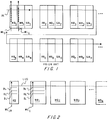
- FIG. 1 illustrates a schematic drawing of a prior art dynamic random access memory (DRAM) redundancy scheme which includes each memory block, labeled MB with an identifying subscript, and a plurality of redundant blocks of memory, RB, each associated with a memory block and carrying the same subscript.
- Each redundant block of memory RB and its associated memory block MB share bit lines (each bit line represent as BL) .
- a plurality of sense amplifiers is also shown in figure 1 with each sense amplifier S/A (hereinafter referred to as sense amp) lying adjacent to and carrying the same subscript as its associated memory block. Redundant blocks of memory serve to provide alternate memory service.
- DRAM dynamic random access memory
- word line WL1 or a memory cell along word line WL1 in memory block MB1 is defective
- word line WL 1R in redundant memory block RB1 is used along with its row (illustrated as verticle columns) of memory cells (each asterisk representing a memory cell).
- a redundancy scheme wherein a redundant array of memory cells are divided into a series of sets. Each set is addressed by a portion of an address corresponding to a location in main memory.
- Each decoder from a group of decoders receives a selected address to be read from or writtten to. In connection with the determination of memory elements needing replacement, one or more of the decoders enables cells from associated redundant sets.
- One block of redundant memory services a plurality of memory blocks from main memory using a common local input/output line.
- the redundant block is relatively smaller in size than each main memory block.
- Each decoder set to flag a particular address for replacement, selects one or more redundant rows of memory from a set of the redundant array according to a portion of the current address.
- Each decoder is assigned memory replacement via designated sets from the redundant array.
- FIG. 1 illustrates a schematic drawing of a prior art dynamic random access memory (DRAM) redundancy scheme.
- DRAM dynamic random access memory
- Figure 2 illustrates a schematic drawing of a first preferred embodiment of the invention's DRAM redundancy scheme.
- Figure 3 illustrates a diagram of a first preferred layout of the invention implementing a 64 megabit DRAM with exploded views of selected components.
- Figure 4 illustrates a diagram of a second preferred layout alternative to that shown in figure 3 for the invention implementing a 64 megabit DRAM.
- Figure 5 illustrates a diagram of one possible scheme showing the use of the signal bits in selecting word lines for refresh.
- Figure 6 illustrates a block diagram of the row redundancy scheme.
- FIG. 2 illustrates a schematic drawing of a first preferred embodiment of the invention's DRAM redundancy scheme.
- Redundant block of memory RB has its own independent bit lines (each labeled BL) unlike that of the prior art in which bit lines of the redundant block and its associated memory block are shared.
- L I/O local input/output
- any word line and memory cells from any of the other blocks can be replaced through the use of redundant block RB.
- the number of wordlines and associated circuitry i.e. memory cells which can be corrected depends on the number of word lines and associated circuitry in the redundant block. Thus, if the redundant block has 5 rows of memory cells, 5 wordlines and their associated cells can be corrected from any of the memory blocks.
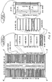
- Figure 3 illustrates a diagram of a first preferred layout of the invention implementing a 64 megabit DRAM with exploded views of selected components.
- an exploded view of a section along the dashed line details one 16 megabit quadrant 2.
- Each 16 megabit quadrant 2 is partitioned into four 4 megabit (4 meg) memory blocks with each block including four 512 kilobit (512k) memory arrays.
- FIG. 1 A section of sense amplifiers S/A.
- a section of sense amplifiers abuts each array.
- the number of bit lines in a 4 meg block is on the order of 2000.
- the labeled 512k array and its associated sense amplifiers S/A are exploded into a more detailed view in which bit lines BLs are of the twisted variety.
- Word line WLINE and bit line YSELECT indicate a word line and a bit line respectively, selected by a respective row decoder and column decoder YDEC.
- the intersection of a bit line with a word line as shown indicates the location of a chosen memory cell.
- the small section of closely spaced vertical lines labeled REDUN BITLINES indicates the bit lines for the redundant memory cells. Bond pads 3 for the address, control, and input/output (I/O) are represented by the small squares down the middle of chip 2. The location of wide data path circuitry is indicated as shown.
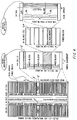
- FIG. 4 A second preferred layout alternative to that shown in figure 3 for the invention implementing a 64 megabit DRAM is illustrated in the diagram in figure 4.
- the position of the redundant blocks differs from that shown in figure 3.
- the redundant blocks are near the column decoders (YDEC). This positioning of the redundant blocks near the column decoders can increase the operating speed of the memory.
- Memory cells of a DRAM must be refreshed to prevent loss of data. Generally, this is accomplished by the word line of a cell being energized so as to allow the cell's bit line to reinsert data to the cell via a sense amplifier. Refresh of a memory cell is required after reading data out of the cell. Refresh is also routinely required to prevent loss of memory storage through capacitor leakage.
- the refresh operation of the preferred embodiment of the 64 meg DRAM is such that 8k of memory cells are refreshed at a time. This translates into four word lines (2k memory cells on each word line) on the 64 meg chip being refreshed at the same time.
- CA PROG Column address program
- CA PROG provides a signal bit either CA or CA_ which allows the selection of four word lines for refresh including any word lines from which the data of an associated cell is desired.
- Figure 5 illustrates a diagram of one possible scheme showing the use of the signal bits in selecting word lines for refresh. Memory cells of two word lines from a pair of diagonally positioned 16 meg qaudrants are refreshed. For instance, when signal bit CA is logic high, signal bit CA_, its complement, is logic low. Consequently, in the scheme shown in figure 5, two word lines in 16 meg quadrant 1 are refreshed along with two word lines in 16 meg quadrant 4.
- signal bit CA_ when signal bit CA_ is logic high, its complement, signal bit CA is logic low, thereby resulting in two word lines in both 16 meg quadrants 2 and 3 being refreshed.
- one of the word lines for a cell selected for refresh will be a word line for a cell selected for reading information therefrom. Refresh of the cells of the selected word line occurs after the selected cell information has been read. Should the row address of a selected cell correspond to an address identified by circuitry (not shown) as having a defective word line, then replacement of the cell with a cell of a redundant word line takes place in accordance with the following description.
- Figure 6 illustrates a block diagram of the row redundancy scheme.
- redundant rows 4 referenced respectively as left and right spare row arrays are each divided into 2 groups of 8 word lines (WLs), 1 group of 16 WLs, and 1 group of 32 WLs.
- Enable circuitry comprising decoders labeled 1, 2, 3, and 4, enables redundant word line blocks labeled 1, 2, 3, and 4 to provide replacement for word line rows of memory within the 4 meg blocks based on signals received from a plurality of laser link decoders.
- enable circuitry can comprise drivers, whereby redundant row selection in spare row arrays is determined by the plurality of laser link decoders. Although only 8 laser link decoders are illustrated in figure 6, fewer or more may be used.
- the redundant memory along word lines are addressable by a portion of the address from the non redundant or rather main memory array.
- the redundant memory can for instance be addressed by 2 to 4 bits which can reflect the least significant 2 to 4 bits in the 12 bit long current address.
- Word line block 1 comprises 32 word lines addressable by row addresses RA0 to RA1.
- Word line block 2 comprises 16 word lines addressable by row addresses RA0 to RA3.
- Word line block 3 comprises 8 word lines addressable by row addresses RA0 to RA2.
- Word line block 4 comprises 8 word lines addressable by row addresses RA0 to RA2.
- either of laser link decoders 1 to 4 could provide replacement of these defective rows with the available 32 word line rows of redundant memory in redundant block 1 addressed by RA0-RA4. If, for instance, in addition to the defective rows 3-10 of the first block, rows 3-10 of a second 4 meg block are defective, decoders 5 or 6 can provide replacement of the defective rows in the second block with redundant rows from the available 16 word line rows of redundant memory in redundant block 2 addressed by RA0-RA3.
- decoder 7 can provide replacement of the defective rows in the third block with redundant rows from the available 8 word line rows of redundant memory in redundant block 3 addressed by RA0-RA2.
- decoder 8 can provide replacement of the defective rows in the fourth block of memory with redundant rows from the available 8 word line rows of redundant memory in redundant block 4 addressed by RA0-RA2.
- redundant word line blocks are in either a right or left spare row array.
- a right or left spare row selection is determined by row address RA11 and its complement RA11_ such that a high signal on an address bit indicates selection of a corresponding spare row array.
- An optimal replacement scheme for the memory can be determined by a computer program 9 (represented in figure 6 as PROG) using linear programming or other techniques. Alternatively, a computer program is not necessary to implement this aspect of the invention. Therefore, a human operator can determine the order of replacement.
Landscapes
- For Increasing The Reliability Of Semiconductor Memories (AREA)
- Dram (AREA)
Applications Claiming Priority (2)
| Application Number | Priority Date | Filing Date | Title |
|---|---|---|---|
| US54007490A | 1990-06-19 | 1990-06-19 | |
| US540074 | 1990-06-19 |
Publications (2)
| Publication Number | Publication Date |
|---|---|
| EP0465808A1 true EP0465808A1 (fr) | 1992-01-15 |
| EP0465808B1 EP0465808B1 (fr) | 1998-07-29 |
Family
ID=24153881
Family Applications (1)
| Application Number | Title | Priority Date | Filing Date |
|---|---|---|---|
| EP91108469A Expired - Lifetime EP0465808B1 (fr) | 1990-06-19 | 1991-05-24 | Schéma de redondance associatif de DRAM avec grandeur de groupe variable |
Country Status (5)
| Country | Link |
|---|---|
| EP (1) | EP0465808B1 (fr) |
| JP (1) | JPH06139795A (fr) |
| KR (1) | KR100196312B1 (fr) |
| CN (1) | CN1058666A (fr) |
| DE (1) | DE69129882T2 (fr) |
Cited By (8)
| Publication number | Priority date | Publication date | Assignee | Title |
|---|---|---|---|---|
| EP0544247A3 (en) * | 1991-11-27 | 1993-10-20 | Texas Instruments Inc | Memory architecture |
| EP0578935A3 (en) * | 1992-07-13 | 1996-10-16 | Samsung Electronics Co Ltd | Row redundancy circuit of a semiconductor memory device |
| EP0869440A1 (fr) * | 1997-03-31 | 1998-10-07 | International Business Machines Corporation | Mémoires tolerantes des fautes et procédé |
| EP0766176A3 (fr) * | 1995-09-29 | 1999-07-14 | Sharp Kabushiki Kaisha | Mémoire morte de remplacement à semi-conducteur |
| EP0892349A3 (fr) * | 1997-07-16 | 2000-02-02 | International Business Machines Corporation | Configuration pour le replacement redondant dans un dispositif de mémoire |
| EP0892350A3 (fr) * | 1997-07-16 | 2000-02-02 | International Business Machines Corporation | Procédé de replacement redondant dans un dispositif de mémoire |
| EP0933709A3 (fr) * | 1998-02-02 | 2000-02-02 | International Business Machines Corporation | Mémoire intégree à semiconducteurs réparable par affectation sélective de groupes de redondance aux domaines |
| KR100546175B1 (ko) * | 1998-10-28 | 2006-04-14 | 주식회사 하이닉스반도체 | 로오 리페어장치 |
Families Citing this family (1)
| Publication number | Priority date | Publication date | Assignee | Title |
|---|---|---|---|---|
| KR100378978B1 (ko) * | 2000-07-21 | 2003-04-08 | 이숙미 | 트랜스글루타미나제를 이용한 콩단백질 필름 및 그 제조방법 |
Citations (4)
| Publication number | Priority date | Publication date | Assignee | Title |
|---|---|---|---|---|
| EP0029322A1 (fr) * | 1979-11-13 | 1981-05-27 | Fujitsu Limited | Dispositif de mémoire à semiconducteur avec redondance |
| US4380066A (en) * | 1980-12-04 | 1983-04-12 | Burroughs Corporation | Defect tolerant memory |
| EP0178950A2 (fr) * | 1984-10-19 | 1986-04-23 | Fujitsu Limited | Dispositif de mémoire à accès aléatoire à transistors bipolaires ayant une configuration à redondance |
| EP0249903A2 (fr) * | 1986-06-12 | 1987-12-23 | Kabushiki Kaisha Toshiba | Dispositif de mémoire à semi-conducteur |
-
1991
- 1991-05-24 DE DE69129882T patent/DE69129882T2/de not_active Expired - Fee Related
- 1991-05-24 EP EP91108469A patent/EP0465808B1/fr not_active Expired - Lifetime
- 1991-06-08 CN CN91103920A patent/CN1058666A/zh active Pending
- 1991-06-18 KR KR1019910010000A patent/KR100196312B1/ko not_active Expired - Lifetime
- 1991-06-19 JP JP3147195A patent/JPH06139795A/ja active Pending
Patent Citations (4)
| Publication number | Priority date | Publication date | Assignee | Title |
|---|---|---|---|---|
| EP0029322A1 (fr) * | 1979-11-13 | 1981-05-27 | Fujitsu Limited | Dispositif de mémoire à semiconducteur avec redondance |
| US4380066A (en) * | 1980-12-04 | 1983-04-12 | Burroughs Corporation | Defect tolerant memory |
| EP0178950A2 (fr) * | 1984-10-19 | 1986-04-23 | Fujitsu Limited | Dispositif de mémoire à accès aléatoire à transistors bipolaires ayant une configuration à redondance |
| EP0249903A2 (fr) * | 1986-06-12 | 1987-12-23 | Kabushiki Kaisha Toshiba | Dispositif de mémoire à semi-conducteur |
Cited By (9)
| Publication number | Priority date | Publication date | Assignee | Title |
|---|---|---|---|---|
| EP0544247A3 (en) * | 1991-11-27 | 1993-10-20 | Texas Instruments Inc | Memory architecture |
| EP0578935A3 (en) * | 1992-07-13 | 1996-10-16 | Samsung Electronics Co Ltd | Row redundancy circuit of a semiconductor memory device |
| EP0766176A3 (fr) * | 1995-09-29 | 1999-07-14 | Sharp Kabushiki Kaisha | Mémoire morte de remplacement à semi-conducteur |
| EP0869440A1 (fr) * | 1997-03-31 | 1998-10-07 | International Business Machines Corporation | Mémoires tolerantes des fautes et procédé |
| KR100295928B1 (ko) * | 1997-03-31 | 2001-08-07 | 포만 제프리 엘 | 내결함성메모리디바이스및그제조방법 |
| EP0892349A3 (fr) * | 1997-07-16 | 2000-02-02 | International Business Machines Corporation | Configuration pour le replacement redondant dans un dispositif de mémoire |
| EP0892350A3 (fr) * | 1997-07-16 | 2000-02-02 | International Business Machines Corporation | Procédé de replacement redondant dans un dispositif de mémoire |
| EP0933709A3 (fr) * | 1998-02-02 | 2000-02-02 | International Business Machines Corporation | Mémoire intégree à semiconducteurs réparable par affectation sélective de groupes de redondance aux domaines |
| KR100546175B1 (ko) * | 1998-10-28 | 2006-04-14 | 주식회사 하이닉스반도체 | 로오 리페어장치 |
Also Published As
| Publication number | Publication date |
|---|---|
| KR100196312B1 (ko) | 1999-06-15 |
| EP0465808B1 (fr) | 1998-07-29 |
| CN1058666A (zh) | 1992-02-12 |
| KR920001555A (ko) | 1992-01-30 |
| DE69129882D1 (de) | 1998-09-03 |
| JPH06139795A (ja) | 1994-05-20 |
| DE69129882T2 (de) | 1999-03-04 |
Similar Documents
| Publication | Publication Date | Title |
|---|---|---|
| US5270976A (en) | Laser link decoder for DRAM redundancy scheme | |
| US6693833B2 (en) | Device and method for repairing a semiconductor memory | |
| US5295101A (en) | Array block level redundancy with steering logic | |
| US5469388A (en) | Row redundancy circuit suitable for high density semiconductor memory devices | |
| US6910152B2 (en) | Device and method for repairing a semiconductor memory | |
| US5491664A (en) | Flexibilitiy for column redundancy in a divided array architecture | |
| KR100443853B1 (ko) | 반도체 메모리 장치 | |
| JP5033887B2 (ja) | 半導体メモリデバイス内のメモリアレイ間で冗長回路を共有するための方法及び装置 | |
| US5495447A (en) | Method and apparatus using mapped redundancy to perform multiple large block memory array repair | |
| JP2919213B2 (ja) | 半導体メモリ装置 | |
| US5675543A (en) | Integrated semiconductor memory device | |
| US5978302A (en) | Multi-bank architecture for a wide I/O DRAM | |
| EP0465808B1 (fr) | Schéma de redondance associatif de DRAM avec grandeur de groupe variable | |
| US7359260B2 (en) | Repair of memory cells | |
| US6407961B1 (en) | Dual access memory array | |
| EP0529330A2 (fr) | Système comportant un décodeur à trajet à laser pour arrangement de redondance pour DRAM | |
| EP0469252B1 (fr) | Décodeur à trajet de laser pour schéma de redondance de DRAM | |
| US6137157A (en) | Semiconductor memory array having shared column redundancy programming | |
| KR100463198B1 (ko) | 데이터 라인 리던던시 스킴을 구비한 반도체 메모리 장치 | |
| US6484277B1 (en) | Integrated memory having a redundancy function | |
| EP0869440B1 (fr) | Mémoires tolerantes des fautes | |
| US6188632B1 (en) | Dual access memory array |
Legal Events
| Date | Code | Title | Description |
|---|---|---|---|
| PUAI | Public reference made under article 153(3) epc to a published international application that has entered the european phase |
Free format text: ORIGINAL CODE: 0009012 |
|
| AK | Designated contracting states |
Kind code of ref document: A1 Designated state(s): DE FR GB IT NL |
|
| 17P | Request for examination filed |
Effective date: 19920715 |
|
| 17Q | First examination report despatched |
Effective date: 19950403 |
|
| GRAG | Despatch of communication of intention to grant |
Free format text: ORIGINAL CODE: EPIDOS AGRA |
|
| GRAG | Despatch of communication of intention to grant |
Free format text: ORIGINAL CODE: EPIDOS AGRA |
|
| GRAH | Despatch of communication of intention to grant a patent |
Free format text: ORIGINAL CODE: EPIDOS IGRA |
|
| GRAH | Despatch of communication of intention to grant a patent |
Free format text: ORIGINAL CODE: EPIDOS IGRA |
|
| GRAA | (expected) grant |
Free format text: ORIGINAL CODE: 0009210 |
|
| AK | Designated contracting states |
Kind code of ref document: B1 Designated state(s): DE FR GB IT NL |
|
| PG25 | Lapsed in a contracting state [announced via postgrant information from national office to epo] |
Ref country code: IT Free format text: LAPSE BECAUSE OF FAILURE TO SUBMIT A TRANSLATION OF THE DESCRIPTION OR TO PAY THE FEE WITHIN THE PRE;WARNING: LAPSES OF ITALIAN PATENTS WITH EFFECTIVE DATE BEFORE 2007 MAY HAVE OCCURRED AT ANY TIME BEFORE 2007. THE CORRECT EFFECTIVE DATE MAY BE DIFFERENT FROM THE ONE RECORDED.SCRIBED TIME-LIMIT Effective date: 19980729 Ref country code: NL Free format text: LAPSE BECAUSE OF FAILURE TO SUBMIT A TRANSLATION OF THE DESCRIPTION OR TO PAY THE FEE WITHIN THE PRESCRIBED TIME-LIMIT Effective date: 19980729 |
|
| REF | Corresponds to: |
Ref document number: 69129882 Country of ref document: DE Date of ref document: 19980903 |
|
| ET | Fr: translation filed | ||
| NLV1 | Nl: lapsed or annulled due to failure to fulfill the requirements of art. 29p and 29m of the patents act | ||
| PLBE | No opposition filed within time limit |
Free format text: ORIGINAL CODE: 0009261 |
|
| STAA | Information on the status of an ep patent application or granted ep patent |
Free format text: STATUS: NO OPPOSITION FILED WITHIN TIME LIMIT |
|
| 26N | No opposition filed | ||
| REG | Reference to a national code |
Ref country code: GB Ref legal event code: IF02 |
|
| PGFP | Annual fee paid to national office [announced via postgrant information from national office to epo] |
Ref country code: DE Payment date: 20070531 Year of fee payment: 17 |
|
| PGFP | Annual fee paid to national office [announced via postgrant information from national office to epo] |
Ref country code: GB Payment date: 20070410 Year of fee payment: 17 |
|
| PGFP | Annual fee paid to national office [announced via postgrant information from national office to epo] |
Ref country code: FR Payment date: 20070503 Year of fee payment: 17 |
|
| GBPC | Gb: european patent ceased through non-payment of renewal fee |
Effective date: 20080524 |
|
| REG | Reference to a national code |
Ref country code: FR Ref legal event code: ST Effective date: 20090119 |
|
| PG25 | Lapsed in a contracting state [announced via postgrant information from national office to epo] |
Ref country code: FR Free format text: LAPSE BECAUSE OF NON-PAYMENT OF DUE FEES Effective date: 20080602 Ref country code: DE Free format text: LAPSE BECAUSE OF NON-PAYMENT OF DUE FEES Effective date: 20081202 |
|
| PG25 | Lapsed in a contracting state [announced via postgrant information from national office to epo] |
Ref country code: GB Free format text: LAPSE BECAUSE OF NON-PAYMENT OF DUE FEES Effective date: 20080524 |