EP0467081A2 - Procédé pour fabriquer un transistor bipolaire - Google Patents
Procédé pour fabriquer un transistor bipolaire Download PDFInfo
- Publication number
- EP0467081A2 EP0467081A2 EP91109976A EP91109976A EP0467081A2 EP 0467081 A2 EP0467081 A2 EP 0467081A2 EP 91109976 A EP91109976 A EP 91109976A EP 91109976 A EP91109976 A EP 91109976A EP 0467081 A2 EP0467081 A2 EP 0467081A2
- Authority
- EP
- European Patent Office
- Prior art keywords
- layer
- auxiliary
- connection
- planar
- planar layer
- Prior art date
- Legal status (The legal status is an assumption and is not a legal conclusion. Google has not performed a legal analysis and makes no representation as to the accuracy of the status listed.)
- Granted
Links
Images




Classifications
-
- H—ELECTRICITY
- H10—SEMICONDUCTOR DEVICES; ELECTRIC SOLID-STATE DEVICES NOT OTHERWISE PROVIDED FOR
- H10W—GENERIC PACKAGES, INTERCONNECTIONS, CONNECTORS OR OTHER CONSTRUCTIONAL DETAILS OF DEVICES COVERED BY CLASS H10
- H10W20/00—Interconnections in chips, wafers or substrates
- H10W20/01—Manufacture or treatment
- H10W20/031—Manufacture or treatment of conductive parts of the interconnections
- H10W20/069—Manufacture or treatment of conductive parts of the interconnections by forming self-aligned vias or self-aligned contact plugs
-
- H—ELECTRICITY
- H10—SEMICONDUCTOR DEVICES; ELECTRIC SOLID-STATE DEVICES NOT OTHERWISE PROVIDED FOR
- H10D—INORGANIC ELECTRIC SEMICONDUCTOR DEVICES
- H10D10/00—Bipolar junction transistors [BJT]
- H10D10/01—Manufacture or treatment
- H10D10/051—Manufacture or treatment of vertical BJTs
-
- H—ELECTRICITY
- H10—SEMICONDUCTOR DEVICES; ELECTRIC SOLID-STATE DEVICES NOT OTHERWISE PROVIDED FOR
- H10D—INORGANIC ELECTRIC SEMICONDUCTOR DEVICES
- H10D64/00—Electrodes of devices having potential barriers
- H10D64/01—Manufacture or treatment
- H10D64/011—Manufacture or treatment of electrodes ohmically coupled to a semiconductor
- H10D64/0111—Manufacture or treatment of electrodes ohmically coupled to a semiconductor to Group IV semiconductors
- H10D64/0113—Manufacture or treatment of electrodes ohmically coupled to a semiconductor to Group IV semiconductors the conductive layers comprising highly doped semiconductor materials, e.g. polysilicon layers or amorphous silicon layers
-
- Y—GENERAL TAGGING OF NEW TECHNOLOGICAL DEVELOPMENTS; GENERAL TAGGING OF CROSS-SECTIONAL TECHNOLOGIES SPANNING OVER SEVERAL SECTIONS OF THE IPC; TECHNICAL SUBJECTS COVERED BY FORMER USPC CROSS-REFERENCE ART COLLECTIONS [XRACs] AND DIGESTS
- Y10—TECHNICAL SUBJECTS COVERED BY FORMER USPC
- Y10S—TECHNICAL SUBJECTS COVERED BY FORMER USPC CROSS-REFERENCE ART COLLECTIONS [XRACs] AND DIGESTS
- Y10S148/00—Metal treatment
- Y10S148/01—Bipolar transistors-ion implantation
-
- Y—GENERAL TAGGING OF NEW TECHNOLOGICAL DEVELOPMENTS; GENERAL TAGGING OF CROSS-SECTIONAL TECHNOLOGIES SPANNING OVER SEVERAL SECTIONS OF THE IPC; TECHNICAL SUBJECTS COVERED BY FORMER USPC CROSS-REFERENCE ART COLLECTIONS [XRACs] AND DIGESTS
- Y10—TECHNICAL SUBJECTS COVERED BY FORMER USPC
- Y10S—TECHNICAL SUBJECTS COVERED BY FORMER USPC CROSS-REFERENCE ART COLLECTIONS [XRACs] AND DIGESTS
- Y10S148/00—Metal treatment
- Y10S148/011—Bipolar transistors
Definitions
- the invention relates to a method for producing a bipolar transistor.
- An oxide spacer is an insulating edge covering that is either produced on the finished base connection before the application of the second polysilicon layer or that is produced on the finished emitter connection before the application of the polysilicon layer for the base connection. In this way, the distance between the base connection and emitter connection becomes independent of the photolithography used.
- the resulting transistors have a very uneven topography, which is a disadvantage in highly integrated circuits.
- Transistors with oxide spacers on the flanks of the base connections are not compatible in their production with advanced techniques such as. B. deposited homo- or heterobases or deposited heteroemitters.
- the pedestal collector consists of an additional implantation of the collector in the active transistor area (see K. Ehinger et al, ESSDERC'89, pp. 797, Springer 1989).
- silicide techniques for both polysilicon layers.
- a silicide must be able to withstand a high temperature step without damaging the device properties.
- the silicide of the base connection must survive an emitter expulsion step without damage.
- the emitter connection is first produced and provided with spacers, the silicide of the emitter connection must survive the temperature steps during the production of the base connection.
- the invention is based on the object of specifying a method for producing planar bipolar transistors in which the risks of yield from etching plasmas are reduced and which is compatible with advanced manufacturing techniques.
- bipolar transistor produced by the manufacturing method according to the invention has a planar surface.
- the base connection, the emitter connection and the collector connection are produced simultaneously from the planar layer in one etching step, there is no etching plasmas exposure and the associated risks of yield in the area for the emitter.
- the dopant concentration in the substrate for the active base region is generated by implantation, diffusion or epitaxial deposition.
- the implantation takes place before the creation of the planar layer.
- the epitaxial deposition also takes place before the planar layer is produced.
- the basic doping is generated by diffusion, this takes place from the planar layer.
- the first auxiliary structure as an implantation mask, it is possible to generate a pedestal collector below the emitter by an additional, high-energy implantation of dopant of the second conductivity type.
- the self-aligned production of the second auxiliary structure to deposit the first auxiliary structure and the exposed areas of the planar layer over the entire area and in conformity with a first auxiliary layer.
- the first auxiliary layer can be selectively etched to the first auxiliary structure and to the planar layer.
- the thickness of the first auxiliary layer is determined so that the surface of the first auxiliary layer has depressions which reflect the shape of the first auxiliary structure.
- a second auxiliary layer is produced on the first auxiliary layer and can be etched selectively to the first auxiliary layer.
- the second auxiliary layer completely covers the surface of the first auxiliary layer and completely fills the depressions in the surface of the first auxiliary layer.
- the second auxiliary layer consists, for. B.
- the second auxiliary structure is produced by etching back the second auxiliary layer until the surface of the first auxiliary layer is exposed outside the recesses and then etching back the exposed parts of the first auxiliary layer down to the underlying surface of the planar layer.
- the width of the gap formed between the first auxiliary structure and the second auxiliary structure is determined by the thickness in which the first auxiliary layer is deposited. Since the deposition of layers with a thickness of 20-500 nm can be precisely controlled, distances of this width are achieved.
- the structure shown in Fig. 1 is produced by the following process steps: in a substrate 1 made of single-crystal, p-doped silicon, a buried collector 2 z. B. generated by implantation of n-doping ions.
- an n-doped epitaxial layer 3 is applied over the entire area.
- Isolation regions 4 and channel stopper regions 5 are produced to separate adjacent transistors in the substrate 1.
- isolation troughs are produced by anisotropic etching after the production of a photoresist mask.
- the isolation trays range z. B. 100 to 500 nm deeper into the substrate 1 than the buried collector 2.
- the channel stopper regions 5 are produced.
- the insulation regions 4 are produced by filling the insulation troughs in a CVD oxide. If necessary, the surface is planarized by etching back.
- This isolation variant which is called BOX isolation, is e.g. B. in T. Shibata et al, IEDM Techn. Dig. 1983, pp. 27-30.
- the manufacture of the buried collector 2, the epitaxial layer 3, the insulation regions 4 and the channel stopper regions 5 can, apart from the box insulation technology described here, also with the aid of the so-called recessed oxide technology, which, for. B. in D. Widmann et al, technology of highly integrated circuits, series semiconductor electronics Vol. 19, Springer 1988, pp. 293-297 is described, or with the help of a trench isolation technology, as z. B. in L. Treitinger et al, Ultrafast Silicon Bipolar Technology, Springer Series in Electronics and Photonics 27, Springer 1988.
- An oxide island 6 is produced in the epitaxial layer 3 (see FIG. 2), which divides the epitaxial layer 3 into an epitaxial island 31 for receiving the later emitter / base region and into a collector connection region 32.
- the collector connection area 32 is z. B. generated by ion implantation and subsequent diffusion with n-doping ions.
- a planar layer 7 is applied to the entire surface of the surface of the insulation regions 4, the epitaxial island 31, the oxide island 6 and the collector connection region 32 (see FIG. 3).
- the planar layer 7 is electrically conductive and of a first conductivity type, e.g. B. p-doped.
- the planar layer 7 consists, for. B. made of polysilicon. You will z. B. deposited in a CVD process amorphous or crystalline in a thickness of 200 nm. The doping takes place either in situ during the deposition or after the deposition by implantation of e.g. B. boron with a dose of 8 x 10 15 cm- 2 and an energy of 10 keV.
- a first layer 8 is applied to the planar layer 7 (see FIG. 3) and can be etched selectively to the planar layer 7.
- the first layer 8 consists, for. B. of silicon oxide and has a thickness of z. B. 50 nm.
- a second layer 9 is applied to the first layer 8, which in turn can be etched selectively with respect to the first layer 8.
- the second layer 9 consists, for. B. made of polysilicon and has a thickness of z. B. 50 nm.
- a third layer 10 is deposited on the second layer 9 and is selectively etchable to the second layer 9.
- the third layer 10 consists, for. B. of silicon oxide and has a thickness of z. B. 200 nm.
- a base zone 11 z. B. by diffusion from the planar layer 7 generated.
- the doping diffused out of the planar layer 7 is compensated for by the opposite, higher doping of the collector connection area 32.
- base zone 11 Other options for producing the base zone 11 are that before the planar layer 7 is deposited, after appropriate masking, an implantation of z. As boron is carried out at a dose of 2.8 x 10 13 cm- 2 and an energy of 5 keV. A further possibility for producing the base zone 11 consists in an epitaxial deposition of the base before the planar layer 7 is produced and a subsequent epitaxial deposition of an emitter zone likewise before the planar layer 7 is produced. Homojunction transistors with e.g. B. 50 nm boron doped base and 50 nm emitter or a heterojunction transistor with z. B.
- a photoresist mask is produced which covers those regions of the third layer 10, below which base connections are provided, while leaving those regions of the surface of the third layer 10 free, below which an emitter connection and a collector connection are provided.
- anisotropic etching e.g. For example, by reactive ion etching with CHF 3/0 2, the third layer 10 is structured of silicon oxide in accordance with the photoresist mask.
- the second layer 9 acts as an etch stop. After completion of the etching and, if necessary, a suitable aftertreatment to remove any etching polymers, the photoresist mask is removed (see FIG. 4).
- the second layer 9 is anisotropic etching, eg. B. structured by reactive ion etching with BCb / Cb.
- the photoresist mask can also be removed at the same time.
- the underlying first layer 8 serves as an etching stop (see FIG. 4).
- the structured third layer 10 and the structured second layer 9 form common flanks.
- the structured second layer 9 forms, together with the structured third layer 10, a first auxiliary structure 12.
- the planar layer 7 By implanting donors, e.g. B. with arsenic with a dose of 2 x 10 16 cm- 2 and an energy of 80 keV, areas of the planar layer 7 are doped for an emitter connection 71 and a collector connection 72 (see FIG. 5). Areas of the planar layer 7 for a base connection 73 are covered by the first auxiliary structure 12. Any further areas of the planar layer 7 that are not covered by the first auxiliary structure 12 must be shielded using an appropriate photoresist mask before the implantation.
- the first layer 8 acts as a scattering oxide (screen oxide) in order to avoid contamination of the planar layer 7 by a neutral particle stream which is mixed with the ion stream during the implantation.
- a pedestal collector 13 is generated below the base zone 11, self-aligned to the emitter connection 71 in the epitaxial island 31 (see FIG. 5).
- the pedestal collector 13 extends into the buried collector 2.
- the pedestal collector 13 improves the collector resistance and thus leads to a performance gain of the finished transistor (see, for example, K. Ehinger et al, ESSDERC'89, pp. 797, Springer 1989).
- the other areas are shielded during high-energy implantation.
- a first auxiliary layer 14 is deposited conformally on the exposed surface and on the flanks of the first auxiliary structure 12 and on the exposed surface of the first layer 8 (see FIG. 6).
- the first auxiliary layer 14 can be selectively etched both to the third layer 10 and to the first layer 8.
- the first auxiliary layer 14 consists, for. B. made of polysilicon and has a thickness of z. B. 50 nm.
- a second auxiliary layer 15 is deposited on the first auxiliary layer 14.
- the second auxiliary layer 15 is deposited in such a way that the depressions in the first auxiliary layer 14 arranged above the emitter connection 71 and the collector connection 72 are completely filled by the second auxiliary layer 15. This is e.g. B.
- the second auxiliary layer 15 consists, for. B. made of silicon oxide. Another possibility of filling the depressions in the surface of the first auxiliary layer 14 is to use a planarizing boron-phosphorus silicate glass as the second auxiliary layer 15.
- the material of the second auxiliary layer 15 is selected such that it can be selectively etched to the first auxiliary layer 14 (see FIG. 6).
- the second auxiliary layer 15 is then anisotropically etched back, so that the surface of the first auxiliary layer 14 is exposed in the region above the base connection 73.
- plug-shaped etching residues 152 plugs remain (see FIG. 7).
- the first auxiliary layer 14 is then anisotropically etched back. This is done e.g. B. in two Sub-steps, with the exposed surface of the first auxiliary layer 14 being removed in a first sub-step (see FIG. 8).
- the surface of the first auxiliary structure 12 acts as an etch stop.
- vertical portions 141 of the first auxiliary layer remain, which are arranged between the first auxiliary structure 12 and the etching residues 152, and covered portions 142, which are arranged between the etching residues 152 and the first layer 8.
- the vertical portions 141 of the first auxiliary layer 14 are removed by anisotropic etching.
- the surface of the first layer 8 acts as an etch stop (see FIG. 9).
- a second auxiliary structure 16 is formed from the etching residues 152 and the underlying, covered portions 142 of the first auxiliary layer 14.
- the second auxiliary structure 16 is self-aligned to the first auxiliary structure 12.
- the distance between the first auxiliary structure 12 and the respectively adjacent portions of the second auxiliary structure 16 is only defined by the width of the etched away vertical portions 141 of the first auxiliary layer 14. This distance therefore depends only on the thickness of the conformally deposited first auxiliary layer 14.
- the first auxiliary structure 12 and the second auxiliary structure 16 are used together as an etching mask for structuring the planar layer 7. This creates the base connection 73, the emitter connection 71 and the collector connection 72.
- the second auxiliary structure 16 covers the emitter connection 71 and the collector connection 72, while the first auxiliary structure 12 covers the base connection 73.
- the distance between the first auxiliary structure 12 and the second auxiliary structure 16 therefore represents the distance between the base connection 73 and the emitter connection 71. According to the above statements, this distance is therefore only set via the thickness of the first auxiliary layer 14.
- the thickness of the first auxiliary layer 14 can be produced in the range of 500-10 nm with an accuracy of 3% -5%.
- the manufacturing method for the first auxiliary structure 12 and the second auxiliary structure 16 ensures that the gaps formed by the etching away of the vertical portions 141 between the first auxiliary structure 12 and the second auxiliary structure 16 are arranged at the edges of the emitter connection 71 and the collector connection 72.
- the planar layer 7 is therefore severed at the edges of the emitter connection 71 and the collector connection 72.
- An anisotropic etch follows in which the exposed silicon oxide, i. H. the etching residues 152, the structured third layer 10 and the exposed parts of the first layer 8 are removed (see FIG. 10).
- the base connection 73 formed is p-doped and the emitter connection 71 and collector connection 72 formed are n-doped. Any diffusion of donors out of the area of the emitter connection 71 and the collector connection 73 before the structuring of the planar layer 7 into the area of the base connection 73 is compensated for by the acceptor doping prevailing in these areas.
- An oxide layer 17 is deposited over the entire surface, so that the gaps between base connection 73, emitter connection 71 and collector connection 72 are closed (see FIG. 12).
- the oxide layer 17 also includes the remnants of the first layer 8.
- a high temperature step follows z. B. 10 sec. At 1050 ° C with the help of fast optical healing (ROA) or 10 min. long at 900 C with the help of furnace annealing.
- ROA fast optical healing
- an emitter zone 18 is formed by diffusion of donors out of the emitter connection 71.
- An inactive base 111 is likewise formed by diffusion out of the base connection 73.
- An active base zone 112 is created between the emitter zone 18 and the pedestal collector 13 (see FIG. 12).
- the bipolar transistor is completed (see FIG. 13).
- the oxide layer 17 is first of all in a back-etching step, e.g. B. with the help of reactive ion etching so far that the surface of the base connection 73, the emitter connection 71 and the collector connection 72 is exposed.
- These exposed areas can be siliconized using a salicide technique. This is done e.g. B. by applying platinum or titanium, then siliconizing and removing the unreacted metallic component.
- a highly conductive layer 19 is selectively produced on the base connection 73, the emitter connection 71 and the collector connection 72 (see FIG. 14).
- the conductive layer 19 can also be produced by CVD deposition of tungsten or CVD deposition of WSi x .
- silicides are no longer subjected to a high-temperature step and therefore immobilization of dopants by compound formation in the silicide or segregation can no longer take place.
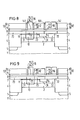
- the finished bipolar transistor is shown in FIG. 15.
- the planar layer 7 can instead of doped polysilicon also from a doped silicide that can withstand the high temperature step to drive out the emitter zone 18, for.
- the first layer 8, second layer 9, third layer 10, first auxiliary layer 14, second auxiliary layer 15 can consist of other, mutually selectively etchable materials instead of the specified materials.
- npn transistor The manufacturing method described for an npn transistor is readily transferable to a pnp transistor.
- the electrical resistance of the base connection 73 made of doped polysilicon can be achieved by an additional implantation of acceptors, e.g. B. Boron can be reduced. In this implantation, an uncritical, phototechnically generated mask is used to shield n-doped regions of the planar layer 7. This step is carried out after the structuring of the planar layer 7 and before the high-temperature step for producing the emitter zone 18.
- acceptors e.g. B. Boron
- an uncritical, phototechnically generated mask is used to shield n-doped regions of the planar layer 7. This step is carried out after the structuring of the planar layer 7 and before the high-temperature step for producing the emitter zone 18.
Landscapes
- Bipolar Transistors (AREA)
Applications Claiming Priority (2)
| Application Number | Priority Date | Filing Date | Title |
|---|---|---|---|
| DE4022892 | 1990-07-18 | ||
| DE4022892 | 1990-07-18 |
Publications (3)
| Publication Number | Publication Date |
|---|---|
| EP0467081A2 true EP0467081A2 (fr) | 1992-01-22 |
| EP0467081A3 EP0467081A3 (en) | 1993-03-31 |
| EP0467081B1 EP0467081B1 (fr) | 1997-06-04 |
Family
ID=6410547
Family Applications (1)
| Application Number | Title | Priority Date | Filing Date |
|---|---|---|---|
| EP91109976A Expired - Lifetime EP0467081B1 (fr) | 1990-07-18 | 1991-06-18 | Procédé pour fabriquer un transistor bipolaire |
Country Status (4)
| Country | Link |
|---|---|
| US (1) | US5217909A (fr) |
| EP (1) | EP0467081B1 (fr) |
| JP (1) | JP3242127B2 (fr) |
| DE (1) | DE59108732D1 (fr) |
Families Citing this family (12)
| Publication number | Priority date | Publication date | Assignee | Title |
|---|---|---|---|---|
| JPH07501181A (ja) * | 1991-10-23 | 1995-02-02 | マイクロユニティ システムズ エンジニアリング,インコーポレイテッド | ベータ特性とパンチスルー特性を改良したバイポーラジャンクショントランジスタ |
| JPH06132298A (ja) * | 1992-10-14 | 1994-05-13 | Mitsubishi Electric Corp | 半導体装置の製造方法 |
| US5369042A (en) * | 1993-03-05 | 1994-11-29 | Texas Instruments Incorporated | Enhanced performance bipolar transistor process |
| JP2551353B2 (ja) * | 1993-10-07 | 1996-11-06 | 日本電気株式会社 | 半導体装置及びその製造方法 |
| JPH07193075A (ja) * | 1993-12-27 | 1995-07-28 | Nec Corp | 半導体装置およびその製造方法 |
| JP2606141B2 (ja) * | 1994-06-16 | 1997-04-30 | 日本電気株式会社 | 半導体装置およびその製造方法 |
| JP3326990B2 (ja) * | 1994-09-26 | 2002-09-24 | ソニー株式会社 | バイポーラトランジスタ及びその製造方法 |
| US6333235B1 (en) * | 2000-04-12 | 2001-12-25 | Industrial Technologyresearch Institute | Method for forming SiGe bipolar transistor |
| US6617220B2 (en) * | 2001-03-16 | 2003-09-09 | International Business Machines Corporation | Method for fabricating an epitaxial base bipolar transistor with raised extrinsic base |
| KR100486304B1 (ko) * | 2003-02-07 | 2005-04-29 | 삼성전자주식회사 | 자기정렬을 이용한 바이씨모스 제조방법 |
| KR100684906B1 (ko) * | 2006-01-03 | 2007-02-22 | 삼성전자주식회사 | 바이폴라 트랜지스터를 갖는 반도체 소자 및 그 형성 방법 |
| US9099489B2 (en) * | 2012-07-10 | 2015-08-04 | Freescale Semiconductor Inc. | Bipolar transistor with high breakdown voltage |
Family Cites Families (6)
| Publication number | Priority date | Publication date | Assignee | Title |
|---|---|---|---|---|
| US4322882A (en) * | 1980-02-04 | 1982-04-06 | Fairchild Camera & Instrument Corp. | Method for making an integrated injection logic structure including a self-aligned base contact |
| JPS56160034A (en) * | 1980-05-14 | 1981-12-09 | Fujitsu Ltd | Impurity diffusion |
| JPS59161867A (ja) * | 1983-03-07 | 1984-09-12 | Hitachi Ltd | 半導体装置 |
| US4997776A (en) * | 1989-03-06 | 1991-03-05 | International Business Machines Corp. | Complementary bipolar transistor structure and method for manufacture |
| JP3024143B2 (ja) * | 1989-06-19 | 2000-03-21 | ソニー株式会社 | 半導体装置の製法 |
| US5024971A (en) * | 1990-08-20 | 1991-06-18 | Motorola, Inc. | Method for patterning submicron openings using an image reversal layer of material |
-
1991
- 1991-06-10 US US07/712,563 patent/US5217909A/en not_active Expired - Lifetime
- 1991-06-18 DE DE59108732T patent/DE59108732D1/de not_active Expired - Fee Related
- 1991-06-18 EP EP91109976A patent/EP0467081B1/fr not_active Expired - Lifetime
- 1991-07-15 JP JP19997191A patent/JP3242127B2/ja not_active Expired - Fee Related
Also Published As
| Publication number | Publication date |
|---|---|
| EP0467081B1 (fr) | 1997-06-04 |
| EP0467081A3 (en) | 1993-03-31 |
| JP3242127B2 (ja) | 2001-12-25 |
| JPH04233236A (ja) | 1992-08-21 |
| US5217909A (en) | 1993-06-08 |
| DE59108732D1 (de) | 1997-07-10 |
Similar Documents
| Publication | Publication Date | Title |
|---|---|---|
| EP0036634B1 (fr) | Procédé de fabrication d'une structure de transistor bipolaire | |
| EP0227970B1 (fr) | Procédé de fabrication simultanée de transistors bipolaires auto-alignés et de transistors de type MOS complémentaires sur un substrat en silicium commun | |
| EP0226892B1 (fr) | Procédé pour la fabrication de transistors bipolaires et MOS-complémentaires sur un substrat commun en silicium | |
| EP0244607B1 (fr) | Méthode pour fabriquer des transistors CMOS optimisés à effet de champ en technologie VLSI | |
| DE19909993B4 (de) | Verfahren zum Bilden von Bipolartransistoren mit selbstausrichtender epitaktischer Basis | |
| DE4445345C2 (de) | Verfahren zur Herstellung eines Bipolartransistors | |
| EP0272433B1 (fr) | Circuit intégré semi-conducteur avec des résistances de charge arrangées sur les régions des oxydes de champ séparant les roues actives des transistors et son mode de fabrication | |
| DE69025805T2 (de) | Herstellen von Halbleitervorrichtungen | |
| EP0118709A2 (fr) | Procédé pour la fabrication de transistor MOS à régions de source et drain planaires, à courte longueur de canal et à niveau de contact auto-aligné comportant un siliciure métallique | |
| DE69430062T2 (de) | Selbstausgerichtetes cmos-verfahren | |
| EP0001550A1 (fr) | Dispositif semiconducteur à intégration avec de petites structures et procédé pour sa fabrication | |
| DE4139490A1 (de) | Bicmos-vorrichtung und verfahren zur herstellung derselben | |
| EP0006510B1 (fr) | Procédé de formation de régions adjacentes et dopées différemment dans un substrat de silicium | |
| EP0226890B1 (fr) | Procédé de fabrication de structures de transistors bipolaires auto-alignés à résistance de base réduite | |
| DE69129379T2 (de) | Verfahren zur Herstellung eines bipolaren Transistors | |
| DE3850847T2 (de) | Selbstjustierter Polysiliziumemitter und Kontaktstruktur für Hochleistungsbipolartransistor. | |
| DE10161058A1 (de) | Halbleiterbauelement und Verfahren zu dessen Herstellung | |
| EP0467081B1 (fr) | Procédé pour fabriquer un transistor bipolaire | |
| DE10002121B4 (de) | Herstellung einer Halbleitervorrichtung mit flachen Sperrschichten | |
| EP0183138A1 (fr) | Procédé pour fabriquer des circuits du type transistors MOS à haute densité | |
| EP0239825B1 (fr) | Procédé de fabrication d'une structure de transistor bipolaire pour des couplages à très hautes vitesses | |
| DE68928787T2 (de) | Verfahren zur Herstellung eines Bipolartransistors | |
| EP1415340A2 (fr) | Procede de fabrication parallele d'un transistor mos et d'un transistor bipolaire | |
| EP1436842B1 (fr) | Transistor bipolaire et procede de fabrication associe | |
| DE3853313T2 (de) | Integrierter Transistor und sein Herstellungsverfahren. |
Legal Events
| Date | Code | Title | Description |
|---|---|---|---|
| PUAI | Public reference made under article 153(3) epc to a published international application that has entered the european phase |
Free format text: ORIGINAL CODE: 0009012 |
|
| AK | Designated contracting states |
Kind code of ref document: A2 Designated state(s): DE FR GB IT |
|
| PUAL | Search report despatched |
Free format text: ORIGINAL CODE: 0009013 |
|
| AK | Designated contracting states |
Kind code of ref document: A3 Designated state(s): DE FR GB IT |
|
| 17P | Request for examination filed |
Effective date: 19930422 |
|
| 17Q | First examination report despatched |
Effective date: 19950809 |
|
| GRAG | Despatch of communication of intention to grant |
Free format text: ORIGINAL CODE: EPIDOS AGRA |
|
| GRAH | Despatch of communication of intention to grant a patent |
Free format text: ORIGINAL CODE: EPIDOS IGRA |
|
| GRAH | Despatch of communication of intention to grant a patent |
Free format text: ORIGINAL CODE: EPIDOS IGRA |
|
| GRAH | Despatch of communication of intention to grant a patent |
Free format text: ORIGINAL CODE: EPIDOS IGRA |
|
| GRAA | (expected) grant |
Free format text: ORIGINAL CODE: 0009210 |
|
| AK | Designated contracting states |
Kind code of ref document: B1 Designated state(s): DE FR GB IT |
|
| REF | Corresponds to: |
Ref document number: 59108732 Country of ref document: DE Date of ref document: 19970710 |
|
| ET | Fr: translation filed | ||
| GBT | Gb: translation of ep patent filed (gb section 77(6)(a)/1977) |
Effective date: 19970806 |
|
| PLBE | No opposition filed within time limit |
Free format text: ORIGINAL CODE: 0009261 |
|
| STAA | Information on the status of an ep patent application or granted ep patent |
Free format text: STATUS: NO OPPOSITION FILED WITHIN TIME LIMIT |
|
| 26N | No opposition filed | ||
| REG | Reference to a national code |
Ref country code: GB Ref legal event code: IF02 |
|
| PGFP | Annual fee paid to national office [announced via postgrant information from national office to epo] |
Ref country code: GB Payment date: 20030530 Year of fee payment: 13 |
|
| PGFP | Annual fee paid to national office [announced via postgrant information from national office to epo] |
Ref country code: FR Payment date: 20030611 Year of fee payment: 13 |
|
| PG25 | Lapsed in a contracting state [announced via postgrant information from national office to epo] |
Ref country code: GB Free format text: LAPSE BECAUSE OF NON-PAYMENT OF DUE FEES Effective date: 20040618 |
|
| GBPC | Gb: european patent ceased through non-payment of renewal fee |
Effective date: 20040618 |
|
| PG25 | Lapsed in a contracting state [announced via postgrant information from national office to epo] |
Ref country code: FR Free format text: LAPSE BECAUSE OF NON-PAYMENT OF DUE FEES Effective date: 20050228 |
|
| REG | Reference to a national code |
Ref country code: FR Ref legal event code: ST |
|
| PG25 | Lapsed in a contracting state [announced via postgrant information from national office to epo] |
Ref country code: IT Free format text: LAPSE BECAUSE OF NON-PAYMENT OF DUE FEES Effective date: 20050618 |
|
| PGFP | Annual fee paid to national office [announced via postgrant information from national office to epo] |
Ref country code: DE Payment date: 20060808 Year of fee payment: 16 |
|
| PG25 | Lapsed in a contracting state [announced via postgrant information from national office to epo] |
Ref country code: DE Free format text: LAPSE BECAUSE OF NON-PAYMENT OF DUE FEES Effective date: 20080101 |