EP0467373A2 - Circuit de compensation du niveau de noir - Google Patents
Circuit de compensation du niveau de noir Download PDFInfo
- Publication number
- EP0467373A2 EP0467373A2 EP91112057A EP91112057A EP0467373A2 EP 0467373 A2 EP0467373 A2 EP 0467373A2 EP 91112057 A EP91112057 A EP 91112057A EP 91112057 A EP91112057 A EP 91112057A EP 0467373 A2 EP0467373 A2 EP 0467373A2
- Authority
- EP
- European Patent Office
- Prior art keywords
- level
- black
- circuit
- signal
- luminance signal
- Prior art date
- Legal status (The legal status is an assumption and is not a legal conclusion. Google has not performed a legal analysis and makes no representation as to the accuracy of the status listed.)
- Granted
Links
Images


Classifications
-
- H—ELECTRICITY
- H04—ELECTRIC COMMUNICATION TECHNIQUE
- H04N—PICTORIAL COMMUNICATION, e.g. TELEVISION
- H04N9/00—Details of colour television systems
- H04N9/64—Circuits for processing colour signals
- H04N9/72—Circuits for processing colour signals for reinsertion of DC and slowly varying components of colour signals
-
- H—ELECTRICITY
- H04—ELECTRIC COMMUNICATION TECHNIQUE
- H04N—PICTORIAL COMMUNICATION, e.g. TELEVISION
- H04N5/00—Details of television systems
- H04N5/14—Picture signal circuitry for video frequency region
- H04N5/20—Circuitry for controlling amplitude response
Definitions
- This invention relates to a black level compensation circuit for compensating a luminance signal.
- a luminance signal 101 is subjected to edge enhancement and amplification by a sharpness circuit 102 and a contrast circuit 103 respectively. Then, it is applied to a black level detection circuit 104 and a pedestal clamp circuit 105. The output signal from the pedestal clamp circuit 105 is applied to a black expansion circuit 106.
- the black level detection circuit 104 detects the blackest level for a given interval and is compared with a given reference level obtained from a pedestal level signal. If the blackest level is larger than the given reference level, the black level expansion circuit 106 does not perform the black-level expansion.
- This black level detection circuit 104 will be described more specifically.
- the luminance signal passing through the contrast circuit 103 (a negative signal) is fed to a differential amplifier having transistors 113 and 107.
- the transistors 108 and 109 controls the differential amplifier having transistors 113 and 107 to operate it for only a period that the luminance signal is received, i.e., scanning period.
- a current source including a transistor 131 and a resistor 132 do not supply a current.
- a current Miller circuit including a transistor 114 and a resistor 115 and another current Miller circuit including a transistor 117 and a resistor 116 allow to flow a current to charge a capacitor 112. That is, a maximum potential of the input signal of the black level detection circuit 104 is maintained at a base of the transistor 107.
- a resistor 118 determines a time constant for maintaining the maximum potential.
- a differential amplifier including transistor 135, resistors 136 and 137, and a transistor 138 compares the maximum potential of the black level with a pedestal level as the given reference level.
- the black expansion circuit 106 expands a tone of black portions of the luminance signal to the pedestal level when the maximum potential is lower than the pedestal level.
- sets of resistors 123 and 125 and a transistor 124; a transistor 126 and a resistor 127; a resistor 128 and a transistor 134; a transistor 129 and a resistor 130; a transistor 131 and a resistor 132 comprise constant current sources respectively.
- the luminance signal inputted to the black level detection circuit 104 from the contrast circuit 103 is subjected to edge enhancement by the sharpness circuit 102 such that at an edge where the luminance signal indicating a shadow level is compensated to show more shadow.
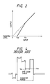
- Fig. 4 shows the luminance signal subjected to edge enhancement.
- an original black level Vbo is changed to Vb1 in level at an edge portion by the sharpness circuit 102.
- the detected blackest level changes with edge enhancement. That is, black compensation changes with sharpness signal.
- the present invention has been developed in order to remove the above-described drawbacks inherent to the conventional black level compensation circuit.
- a black compensation circuit for compensating a luminance signal, comprising: a black-level expanding circuit responsive to a control signal and the luminance signal for performing expansion of a tone of a black portion of the luminance signal and for performing conversion of the luminance signal into a black-level expanded signal in the absence of the control signal; a low-pass filter circuit for low-pass filtering the luminance signal to remove high frequency components; a detection circuit responsive to an output of the low-pass filter circuit for detecting the blackest level for a given interval; and a comparing circuit for comparing the blackest level with a given level to produce the control signal, thereby the black-level expanding circuit stopping the expansion and the conversion in the presence of the control signal.
- a black compensation circuit for compensating a luminance signal, comprising: a black-level expanding circuit responsive to a control signal and the luminance signal for performing expansion of a tone of a black portion of the luminance signal and for performing conversion of the luminance signal into a black-level expanded signal in the absence of the control signal; a low-pass filter circuit for low-pass filtering the output signal of the black-level expanding circuit to remove high frequency components; a detection circuit responsive to an output of the low-pass filter circuit for detecting the blackest level for a given interval; and a comparing circuit for comparing the blackest level with a given level to produce the control signal, thereby the black-level expanding circuit stopping the expansion and the conversion in the presence of the control signal.
- the blackest level does not change with sharpness because the luminance signal subjected to edge enhancement is passed through the low-pass filter, then, it is sent to the detection circuit.
- Fig. 1 is a schematic circuit diagram of the first embodiment of a black level compensation circuit of the invention.
- a luminance signal 1 is applied to a sharpness circuit 2.
- An output of the sharpness circuit 3 is sent to a contrast circuit 3.
- An output of the contrast circuit 3 is fed to a low-pass filter 40 and a pedestal clamp circuit 5.
- An output of the pedestal clamp circuit 5 is sent to a black level expansion circuit 6.
- the sharpness circuit 2 performs edge enhancement to improve picture quality.
- the contrast circuit 3 controls an amplitude of the luminance signal to a given range.
- the pedestal clamp circuit 5 determines brightness of the output of the contrast circuit 3 and sends it to the black level expansion circuit 6.
- the output of the contrast circuit 3 sent to a low-pass filter 40 of 1-2 MHz comprises a resistor 7 and a capacitor 8 to remove high frequency components to decrease the affection of edge enhancement.
- An output of the low-pass filter 40 is sent to the black level detection circuit 4.
- the black level detection circuit 4 detects the blackest level for a given interval and is compared with a pedestal level signal as a given reference level. If the blackest level is larger than the given reference level, the black level expansion circuit 6 does not perform the black-level expansion. That is, if the luminance signal is of a short range signal, the black-level expansion is carried out. On the other hand, if the luminance signal is of a long range signal, the black-level expansion is stopped.
- This black level detection circuit 4 will be described more specifically.
- the signal passing through the contrast circuit 3 (a negative signal) is fed through the low-pass filter 40 to a differential amplifier having transistors 13 and 14.
- the transistors 35 and 36 controls the differential amplifier having transistors 13 and 14 to operate it for only the period that the luminance signal is received, i.e., scanning period.
- a current source including a transistor 31 and a resistor 32 do not supply a current.
- the transistor 13 turns on.
- a current Miller circuit including a transistor 15 and a resistor 16 and another current Miller circuit including a transistor 18, and a resistor 17 allow to flow a current which charges a capacitor 10.
- a maximum potential i.e., the blackest level of the input signal is maintained at a base of the transistor 14.
- a resistor 9 connected to the capacitor 10 in parallel determines a time constant for maintaining the maximum potential as a given interval.
- a differential amplifier including a transistor 11, resistors 12 and 13a, and a transistor 14a compares the maximum potential level of the black level with a pedestal level, which acts as a comparator.
- An output of the differential amplifier including a transistor 11, resistors 12 and 13a is sent to the black level expansion circuit 6 through I-V converter for converting a current of the output signal from this differential amplifier into a voltage output.
- the black level expansion circuit 6 expands a tone of a black portion of the luminance signal and converts the luminance signal into black-level expanded signal when the maximum potential is not lower than the pedestal level as a given reference level. When it is larger than the given reference level expansion circuit 6 stops this black level expansion.
- Fig. 2 shows a relation between input and output of the black the expansion circuit 6. Between input levels Vst and Vbl a characteristic curve of the output of the black level expansion circuit 6 is bent to compression of the range in the presence of the control signal from the comparing circuit. In the absence of the control signal, the black level expansion circuit expands its output range as shown by the chain line in Fig. 2. As the result, black portions in reproduced picture image are compensated to be more dark, so that the crisp picture is obtained. In this case, a stable black level can be obtained because a change of the input signal by sharpness circuit is removed by the low-pass filter 40.
- Resistors 24 and 26 and a transistor 25; a transistor 27 and a resistor 28; a resistor 29 and transistor 30; a transistor 31 and a resistor 32; and a transistor 33 and a resistor 34 are constant current sources respectively.
- H blanking signal is applied to the transistor 35.
- V blanking signal is fed to a transistor 36.
- numerals 15 to 37 operate in the same way as elements 108, 109, 114-117, 123-134, and 139-143 of the prior art.
- the input luminance signal 1 may include a large amount of noise component.
- the low-pass filter reduces the noise component and provides a stable black compensation.
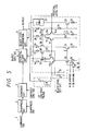
- Fig. 5 is a schematic circuit diagram of the second embodiment of a black level compensation circuit of the invention.
- a luminance signal 1 is applied to a sharpness circuit 2.
- An output of the sharpness circuit 3 is sent to a contrast circuit 3.
- An output of the contrast circuit 3 is fed to a pedestal clamp circuit 5.
- An output of the pedestal clamp circuit 5 is sent to a black level expansion circuit 6.
- the sharpness circuit 2 performs edge enhancement to improve picture quality.
- the contrast circuit 3 controls an amplitude of the luminance signal to a given range.
- the pedestal clamp circuit 5 determines brightness of the output of the contrast circuit 3 and sends it to the black level expansion circuit 6.
- the output of the black level expansion circuit 6 sent to a low-pass filter 40 of 1-2 MHz comprises a resistor 7 and a capacitor 8 to remove high frequency components to decrease the affection of edge enhancement.
- An output of the low-pass filter 40 is sent to the black level detection circuit 4.
- the black level detection circuit 4 detects the blackest level for a given interval and is compared with a pedestal level signal as a given reference level. If the blackest level is larger than the given reference level, the black level expansion circuit 6 does not perform the black-level expansion. That is, if the luminance signal is of a short range signal, the black-level expansion is carried out. On the other hand, if the luminance signal is of a long range signal, the black-level expansion is stopped.
- the black level expansion circuit 6 expands its output range. As the result, black portions in reproduced picture image are compensated to be more dark, so that the crisp picture is obtained. In this case, a stable black level can be obtained because a change of the input signal by sharpness circuit is removed by the low-pass filter 40.
Landscapes
- Engineering & Computer Science (AREA)
- Multimedia (AREA)
- Signal Processing (AREA)
- Picture Signal Circuits (AREA)
- Processing Of Color Television Signals (AREA)
Applications Claiming Priority (2)
| Application Number | Priority Date | Filing Date | Title |
|---|---|---|---|
| JP189470/90 | 1990-07-19 | ||
| JP2189470A JP2599020B2 (ja) | 1990-07-19 | 1990-07-19 | 黒レベル補正回路 |
Publications (3)
| Publication Number | Publication Date |
|---|---|
| EP0467373A2 true EP0467373A2 (fr) | 1992-01-22 |
| EP0467373A3 EP0467373A3 (en) | 1992-12-09 |
| EP0467373B1 EP0467373B1 (fr) | 1996-03-06 |
Family
ID=16241806
Family Applications (1)
| Application Number | Title | Priority Date | Filing Date |
|---|---|---|---|
| EP91112057A Expired - Lifetime EP0467373B1 (fr) | 1990-07-19 | 1991-07-18 | Circuit de compensation du niveau de noir |
Country Status (7)
| Country | Link |
|---|---|
| US (1) | US5262862A (fr) |
| EP (1) | EP0467373B1 (fr) |
| JP (1) | JP2599020B2 (fr) |
| KR (1) | KR950007929B1 (fr) |
| CA (1) | CA2047371C (fr) |
| DE (1) | DE69117603T2 (fr) |
| MY (1) | MY107706A (fr) |
Cited By (2)
| Publication number | Priority date | Publication date | Assignee | Title |
|---|---|---|---|---|
| EP0599398A3 (en) * | 1992-11-24 | 1994-06-22 | Philips Patentverwaltung | Video signal processing circuit. |
| WO2000075916A1 (fr) * | 1999-06-07 | 2000-12-14 | Seiko Epson Corporation | Appareil et procede d'affichage d'image, et dispositif et procede de traitement d'image |
Families Citing this family (5)
| Publication number | Priority date | Publication date | Assignee | Title |
|---|---|---|---|---|
| US5391944A (en) * | 1992-01-22 | 1995-02-21 | Matsushita Electric Industrial Co., Ltd. | Image-tone control circuit and gradient adjusting circuit therefor |
| KR100346840B1 (ko) * | 1999-11-04 | 2002-08-03 | 삼성전자 주식회사 | 화면의 펄럭거림을 최소화하는 흑신장 장치 및 그 방법 |
| JP3844430B2 (ja) * | 2001-06-26 | 2006-11-15 | 三菱電機株式会社 | 映像信号処理装置および映像信号処理方法 |
| JP3722740B2 (ja) * | 2001-11-05 | 2005-11-30 | 三菱電機株式会社 | 映像処理装置及び映像処理方法 |
| JP4740044B2 (ja) * | 2006-06-06 | 2011-08-03 | 河村電器産業株式会社 | 機器収納キャビネット |
Family Cites Families (6)
| Publication number | Priority date | Publication date | Assignee | Title |
|---|---|---|---|---|
| FR2406922A1 (fr) * | 1977-10-21 | 1979-05-18 | Thomson Csf | Dispositif d'expansion de contraste video et systeme comportant un tel dispositif |
| JPS6043972A (ja) * | 1983-08-22 | 1985-03-08 | Sony Corp | 映像の黒レベル再生回路 |
| FR2606956A1 (fr) * | 1986-11-14 | 1988-05-20 | Radiotechnique Compelec | Dispositif de conversion analogique-numerique comportant un dispositif de controle automatique de gain |
| JP2748442B2 (ja) * | 1988-10-13 | 1998-05-06 | ソニー株式会社 | カラー映像信号の処理装置 |
| US4937671A (en) * | 1988-12-28 | 1990-06-26 | Zenith Electronics Corporation | Digital video black expander |
| US4975773A (en) * | 1989-03-31 | 1990-12-04 | Zenith Electronics Corporation | Dynamic range video black level expander |
-
1990
- 1990-07-19 JP JP2189470A patent/JP2599020B2/ja not_active Expired - Fee Related
-
1991
- 1991-07-18 DE DE69117603T patent/DE69117603T2/de not_active Expired - Fee Related
- 1991-07-18 CA CA002047371A patent/CA2047371C/fr not_active Expired - Fee Related
- 1991-07-18 EP EP91112057A patent/EP0467373B1/fr not_active Expired - Lifetime
- 1991-07-18 US US07/732,000 patent/US5262862A/en not_active Expired - Fee Related
- 1991-07-19 KR KR1019910012360A patent/KR950007929B1/ko not_active Expired - Fee Related
- 1991-07-19 MY MYPI91001300A patent/MY107706A/en unknown
Cited By (4)
| Publication number | Priority date | Publication date | Assignee | Title |
|---|---|---|---|---|
| EP0599398A3 (en) * | 1992-11-24 | 1994-06-22 | Philips Patentverwaltung | Video signal processing circuit. |
| WO2000075916A1 (fr) * | 1999-06-07 | 2000-12-14 | Seiko Epson Corporation | Appareil et procede d'affichage d'image, et dispositif et procede de traitement d'image |
| US7570237B2 (en) | 1999-06-07 | 2009-08-04 | Seiko Epson Corporation | Method and apparatus for adjusting quality of a displayed image |
| US8537085B2 (en) | 1999-06-07 | 2013-09-17 | Seiko Epson Corporation | Method and apparatus for adjusting quality of a displayed image |
Also Published As
| Publication number | Publication date |
|---|---|
| KR920003787A (ko) | 1992-02-29 |
| JPH0479482A (ja) | 1992-03-12 |
| JP2599020B2 (ja) | 1997-04-09 |
| EP0467373A3 (en) | 1992-12-09 |
| EP0467373B1 (fr) | 1996-03-06 |
| CA2047371A1 (fr) | 1992-01-20 |
| DE69117603D1 (de) | 1996-04-11 |
| US5262862A (en) | 1993-11-16 |
| KR950007929B1 (ko) | 1995-07-21 |
| MY107706A (en) | 1996-05-30 |
| CA2047371C (fr) | 1995-12-05 |
| DE69117603T2 (de) | 1996-07-25 |
Similar Documents
| Publication | Publication Date | Title |
|---|---|---|
| US4926261A (en) | Video noise reduction circuit | |
| CA1220851A (fr) | Circuit de retablissement du niveau du noir | |
| US5262862A (en) | Black level compensation circuit for a luminance signal | |
| US3947631A (en) | Automatic video signal control circuit | |
| GB2053599A (en) | Automatic gain control circuit | |
| EP0467223A1 (fr) | Circuit pour détecter le niveau moyen d'un signal d'image | |
| US3214517A (en) | Automatic control circuit for television receivers | |
| CA1106491A (fr) | Circuit de blocage | |
| JP4074712B2 (ja) | モニタの画面輝度調整部 | |
| JP2856787B2 (ja) | 2値化回路、中間レベル検出回路及びピーク包絡線検出回路 | |
| JPH09214844A (ja) | 可変ifゲイン制御を行うif復調器回路 | |
| KR960007562Y1 (ko) | 자동이득제어회로 | |
| JPH06245100A (ja) | 映像信号処理装置 | |
| KR950011306B1 (ko) | 수직다이나믹포커스회로 | |
| KR910000546Y1 (ko) | 비데오 카메라의 암전류 보정회로 | |
| JPH04314279A (ja) | Agc回路 | |
| KR950010890B1 (ko) | 영상신호 자동이득제어장치 | |
| KR0122946Y1 (ko) | 모니터의 뮤트회로 | |
| KR890004962Y1 (ko) | 윤곽 보정 신호의 이득 조절회로 | |
| JP2538366B2 (ja) | ビデオト―ン回路 | |
| KR100193579B1 (ko) | 복합 영상기기의 영상 노이즈 제거회로 | |
| JPS60109316A (ja) | 利得制御回路 | |
| JPH06339046A (ja) | クランプ回路 | |
| KR950010063B1 (ko) | 영상신호의 자동 이득 조절 및 클램핑 회로 | |
| KR980007790A (ko) | 텔레비젼 수상기의 자동화질 보정회로 |
Legal Events
| Date | Code | Title | Description |
|---|---|---|---|
| PUAI | Public reference made under article 153(3) epc to a published international application that has entered the european phase |
Free format text: ORIGINAL CODE: 0009012 |
|
| 17P | Request for examination filed |
Effective date: 19910718 |
|
| AK | Designated contracting states |
Kind code of ref document: A2 Designated state(s): DE GB |
|
| PUAL | Search report despatched |
Free format text: ORIGINAL CODE: 0009013 |
|
| AK | Designated contracting states |
Kind code of ref document: A3 Designated state(s): DE GB |
|
| 17Q | First examination report despatched |
Effective date: 19940927 |
|
| GRAH | Despatch of communication of intention to grant a patent |
Free format text: ORIGINAL CODE: EPIDOS IGRA |
|
| GRAA | (expected) grant |
Free format text: ORIGINAL CODE: 0009210 |
|
| AK | Designated contracting states |
Kind code of ref document: B1 Designated state(s): DE GB |
|
| REF | Corresponds to: |
Ref document number: 69117603 Country of ref document: DE Date of ref document: 19960411 |
|
| PLBE | No opposition filed within time limit |
Free format text: ORIGINAL CODE: 0009261 |
|
| STAA | Information on the status of an ep patent application or granted ep patent |
Free format text: STATUS: NO OPPOSITION FILED WITHIN TIME LIMIT |
|
| 26N | No opposition filed | ||
| REG | Reference to a national code |
Ref country code: GB Ref legal event code: IF02 |
|
| PGFP | Annual fee paid to national office [announced via postgrant information from national office to epo] |
Ref country code: GB Payment date: 20050713 Year of fee payment: 15 |
|
| PGFP | Annual fee paid to national office [announced via postgrant information from national office to epo] |
Ref country code: DE Payment date: 20050714 Year of fee payment: 15 |
|
| PG25 | Lapsed in a contracting state [announced via postgrant information from national office to epo] |
Ref country code: GB Free format text: LAPSE BECAUSE OF NON-PAYMENT OF DUE FEES Effective date: 20060718 |
|
| PG25 | Lapsed in a contracting state [announced via postgrant information from national office to epo] |
Ref country code: DE Free format text: LAPSE BECAUSE OF NON-PAYMENT OF DUE FEES Effective date: 20070201 |
|
| GBPC | Gb: european patent ceased through non-payment of renewal fee |
Effective date: 20060718 |