EP0467374A2 - Circuit de régulation pour un onduleur pouvant fonctionner en mode individuel et en mode connecté - Google Patents
Circuit de régulation pour un onduleur pouvant fonctionner en mode individuel et en mode connecté Download PDFInfo
- Publication number
- EP0467374A2 EP0467374A2 EP91112058A EP91112058A EP0467374A2 EP 0467374 A2 EP0467374 A2 EP 0467374A2 EP 91112058 A EP91112058 A EP 91112058A EP 91112058 A EP91112058 A EP 91112058A EP 0467374 A2 EP0467374 A2 EP 0467374A2
- Authority
- EP
- European Patent Office
- Prior art keywords
- voltage
- phase
- invertor
- component
- vector
- Prior art date
- Legal status (The legal status is an assumption and is not a legal conclusion. Google has not performed a legal analysis and makes no representation as to the accuracy of the status listed.)
- Granted
Links
Images



Classifications
-
- H—ELECTRICITY
- H02—GENERATION; CONVERSION OR DISTRIBUTION OF ELECTRIC POWER
- H02M—APPARATUS FOR CONVERSION BETWEEN AC AND AC, BETWEEN AC AND DC, OR BETWEEN DC AND DC, AND FOR USE WITH MAINS OR SIMILAR POWER SUPPLY SYSTEMS; CONVERSION OF DC OR AC INPUT POWER INTO SURGE OUTPUT POWER; CONTROL OR REGULATION THEREOF
- H02M7/00—Conversion of AC power input into DC power output; Conversion of DC power input into AC power output
- H02M7/42—Conversion of DC power input into AC power output without possibility of reversal
- H02M7/44—Conversion of DC power input into AC power output without possibility of reversal by static converters
- H02M7/48—Conversion of DC power input into AC power output without possibility of reversal by static converters using discharge tubes with control electrode or semiconductor devices with control electrode
Definitions
- the present invention relates to a control circuit for a voltage invertor operable in an individual mode in which the invertor converts a DC voltage from a DC source, such as a fuel cell, a solar cell, and a battery, to an AC voltage, and individually transfers the converted AC voltage to an AC load, and in an interconnection mode in which the invertor power system is interconnected with or incorporated into a power system, the converted AC voltage, together with the power voltage of the power system, is transferred to the load. More particularly, the present invention relates to a control circuit for the voltage invertor, which includes a compensating means for compensating an instantaneous variation of the power system voltage.
- the control circuit for the voltage invertor operable in the individual and interconnection modes comprises a constant voltage control system provided for use in the individual mode, and an effective power control system and a reactive power control system both provided for use in the interconnection mode.
- the invertor control circuit is provided with a synchronous-interconnection control system including phase and voltage (amplitude) adjusters, or an adjuster for adjusting those items of the output voltage.
- the synchronous-interconnection control system is used for a power system synchronous operation, which is performed when the invertor changes its operation mode from the individual mode to the interconnection mode.
- the synchronous-interconnection control system including the phase and voltage (amplitude) adjusters, stops those adjusters after the invertor power system is interconnected with the power system, and operates an effective power adjuster of the effective power control system and a reactive power adjuster of the reactive power control system.
- the synchronous-interconnection control system and the effective and reactive power control systems are selectively changed over before and after the invertor power system is interconnected with the power system.
- Fig. 4 is a block diagram showing a general circuit arrangement of the control circuit for voltage invertor operable in the individual and interconnection modes.
- reference numeral 1 designates a self-exciting voltage invertor; 2, an output reactor of the invertor 1; 3, a power system with which the invertor power system is interconnected; 4, a load; 5 a breaker for the interconnection mode; 6, a load breaker; 7, a voltage detect transformer (PT); and 8 a current detect transformer (CT).
- PT voltage detect transformer
- CT current detect transformer
- An individual operation control system 10 includes a voltage adjuster 10B for adjusting a detection voltage Vid detected by a voltage detector 9 to approach to a value set by a voltage setter 10A.
- the control system applies the output voltage of the voltage adjuster 10B through a selector 42 to a pulse generation-amplifier (PA) 30, which is provided for applying a striking pulse to the invertor 1.
- PA pulse generation-amplifier
- the same applies a fixed frequency signal generated by an oscillator 11 through another selector 45 to the pulse generation-amplifier PA. Consequently, the invertor 1 transfers an AC power of which the reference frequency is the fixed frequency of the oscillator 11, to the load 4 through the load breaker 6.
- An interconnected power system in which the power system of the invertor 1 is interconnected, for AC power transmission, with the power system 3, through the breaker 5, comprises an effective power control system 12 including a effective power adjuster 12B, and a reactive power control system 15 including a reactive power adjuster 15B.
- An effective-reactive power detector 14 receives and separates the AC power into an effective component P and a reactive component Q.
- the effective power adjuster 12B controls the output voltage of the invertor so as to make the detected effective component P approach to a set value set by an effective power setter 12A.
- the reactive power control system 15 controls the output voltage of the invertor so as to make the detected reactive component Q approach to a set value set by a reactive power setter 15A.
- a current/voltage (I/V) converter 31 converts the outputs of each control system into voltages corresponding to the output voltage of the invertor 1.
- the output voltages of the converter 31 are applied respectively through the selectors 41 and 42, to the pulse generation-amplifier (PA) 30.
- PA pulse generation-amplifier
- a selector 45 is turned to a contact 45B so that the reference output frequency of the invertor 1 is controlled so as to be equal to the frequency of the power system 3.
- the output control signal of the voltage setter 10A is supplied through the contact 41 B to the pulse generation-amplifier 30.
- a phase difference q) between the invertor output voltage and the power system voltage is detected by a phase difference detector 21.
- a phase-difference adjuster 20B contained in the synchronous-interconnection control circuit, controls the reactive component of the invertor 1 so as to make the phase difference q) approach to a value that is set by a phase-difference setter 20A (normally, it is set at 0).
- the output signal of the phase-difference adjuster 20B is supplied to the pulse generation-amplifier 30, through the contact 42B of the selector 42.
- the breaker 5 In the individual mode, the breaker 5 is opened, and the respective selectors are turned to the contacts 41 B, 42B, and 45A. Under this condition, an AC power of which, the voltage is controlled by the voltage adjuster 10B and the frequency is controlled by the oscillator 11, is supplied through the load breaker 6 to the load.
- the synchronous-interconnection control is performed in a manner that the selector 45 is turned to the contact 45B, the amplitude (instantaneous value) and the phase of the output voltage of the invertor 1 are made to approach to those values of the voltage of the power system 3, by the synchronous-interconnection control circuit 20, and thereafter, the breaker 5 is closed.
- the interconnection power system operation is performed by activating the effective power control system 12 and the reactive power control system 15 and turning the selectors to the contacts 41 A and 42A.
- the control circuit of the invertor containing a proportional integration adjuster (PI adjuster) as a main component, is based on the fixed value control technique which operates to keep a set value at a fixed value against incoming disturbance.
- PI adjuster proportional integration adjuster
- the present invention is to provide a control circuit for invertor, which is capable of compensating an instantaneous variation of the power system without decreasing of the stability of the control circuit upon the synchronous-interconnection mode being in advance of interconnection mode.
- the present invention provides a control circuit for an invertor operable in an individual mode and an interconnection mode, having an individual operation control system in which a control system for a voltage invertor for converting DC voltage to AC voltage, controls AC voltage in a constant-voltage and individually supplies the converted AC voltage to a load, a synchronous-interconnection control system for controlling the amplitude and phase of the output voltage of the invertor for synchronization them with those in a power system to incorporate the invertor into the power system; and effective and reactive power control systems for controlling the effective component and the reactive component of an electric power transferred between the power system and the invertor interconnected with the power system, thereby to perform the interconnection mode operation; the control circuit serving also as a voltage adjuster for making a constant-voltage control or a synchronous control of the AC voltage, characterized in that the control circuit comprises a synchronous compensating circuit in which when the invertor is operating in a power system synchronous operation mode under control of the synchronous-interconnection
- the control circuit for the invertor comprises an interconnection mode compensating circuit in which the output voltage of the invertor, which is operating in the interconnection mode under control of the effective power control system and the reactive power control system, is stored as an internal vector, a quantity of an instantaneous variation in the voltage of the power system is detected in terms of a quantity of a variation of the component in phase with the internal vector and a quantity of a variation of the component orthogonal to the internal vector, and the detected variation quantities are respectively added to the voltage-converted outputs of the effective power control system and the reactive power control system.
- the control circuit for the invertor may comprise a synchronous-interconnection mode compensating circuit in which the output voltage of the invertor, which is operating in the power system synchronous-interconnection mode or the interconnection mode, is stored as an internal vector, a quantity of an instantaneous variation in the voltage of the power system is detected in terms of a quantity of a variation of the component in phase with the internal vector and a quantity of a variation of the component orthogonal to the internal vector, and the detected variation quantities are respectively added to the outputs of the effective power control system and the reactive power control system or the outputs of the synchronous-interconnection control system.
- the first aspect of the present invention includes a synchronous compensating circuit.
- the compensating circuit when the invertor is operating in the power system synchronous operation mode, which is followed by the interconnection mode, an instantaneous voltage variation occurring in the power system is detected in terms of the component in phase with a reference voltage vector as the vector of the output voltage of the invertor, and the variation of component orthogonal to the reference voltage vector.
- the detected variations are respectively added to the outputs of a voltage adjuster and a phase adjuster in the synchronous-interconnection control system.
- the amplitude and the phase of the output voltage of the invertor, when the power system synchronous-interconnection is set up, can be compensated following the instantaneous voltage variation in the power system. Further, the synchronous-interconnection control system does not need to follow the instantaneous voltage variation in the power system. Therefore, the fixed value control function, which is the function proper to the PI adjuster, can be stably maintained.
- a quantity of an instantaneous variation in the voltage of the power system when the invertor is operating in the interconnection mode, is detected in terms of a quantity of a variation of the component in phase with the internal vector and a quantity of a variation of the component orthogonal to the internal vector, and the detected variation quantities are respectively added to the outputs of the effective power control system and the reactive power control system. Therefore, with a response delay of the synchronous signal generator (PLL circuit) containing a memory element, an instantaneous variation of the voltage vector is compared with the internal vector before the variation occurs, thereby to detect a quantity of the variation.
- PLL circuit synchronous signal generator
- a quantity of an instantaneous variation in the voltage of the power system is detected in terms of a quantity of a variation of the component in phase with the internal vector and a quantity of a variation of the component orthogonal to the internal vector, and the detected variation quantities are respectively added to the outputs of the effective power control system and the reactive power control system or the outputs of the synchronous-interconnection control system.
- the compensating circuit thus arranged controls the output voltages of both the control systems according to an instantaneous variation in the power system voltage.
- control circuit can control, in accordance with an instantaneous variation of the power system voltage, both the invertor output voltage at the time of setting up the synchronous operation mode, and the invertor output voltage at the time of setting up the interconnection mode. Accordingly, a stable fixed-value control can be secured while lessening the control processing loads of both the control systems.
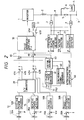
- Fig. 1 is a block diagram showing a control circuit for an invertor operable in the individual mode and the interconnection mode, which is an embodiment of a first invention of the present invention.
- like reference symbols are used for designating like or equivalent portions in the drawing showing the conventional circuit, for simplicity. It is assumed that the load breaker 6 is open, the selectors 41, 42, and 45 are turned to the B contacts, and the power system synchronous operation is being performed under control of the voltage adjuster 10B and the phase-difference adjuster 20B, which serve as the PI adjuster in the synchronous-interconnection control system.
- a synchronous compensating circuit 50 is made up a pair of 3-phase/2-phase converters 51 and 52, a vector analyzer 53, a vector drainer 54, an adder 55, and another adder 56.
- the 3-phase/2-phase converter 51 separates the output voltage Vi of the invertor 1 into an in-phase component and an orthogonal component.
- the 3-phase/2-phase converter 52 likewise separates the voltage Vs of the power system 3 into an in-phase component and an orthogonal component.
- the vector analyzer 53 is provided for preparing a reference vector of the invertor voltage on the basis of the output voltage of the converter 51.
- the vector drainer 54 separates a quantity of a variation of the output voltage of the converter 52 with respect to the reference vector into two components, an in-phase component, which is in phase with the reference vector, and an orthogonal component, which is orthogonal to the reference vector.
- the adder 55 adds the detected in-phase component to the output voltage of the voltage ad juster 10B.
- the adder 56 adds a variation quantity of the detected orthogonal component to the output voltage of the phase-difference adjuster 20B.
- the control circuit including the synchronous compensating circuit 50 if an instantaneous variation occurs in the amplitude and the phase of the voltage Vs of the power system 3, the voltage adjuster 10B and the phase-difference adjuster 20B, which constitute the PI adjuster, cannot follow a changing speed of the instantaneous variation.
- the amplitude and the phase of the output voltage Vi of the invertor 1 become different from those of the power system voltage Vs of the power system 3, respectively.
- the synchronous compensating circuit 50 detects the instantaneous variation with respect to the output voltage vector of the invertor.
- the in-phase component and the orthogonal component, that are detected are differences between the changing speed of the instantaneous variation and a response speed of the voltage adjuster 10B, and between the changing speed and a response speed of the phase-difference adjuster 20B.
- the differences are added to the output voltages of the adjusters. Accordingly, the output voltage of the invertor 1 varies in synchronism with the instantaneous variation of the voltage of the power system.
- a stable synchronous-interconnection state is set up, and a stable synchronous operation is performed while placing the voltage adjuster and the phase-difference adjuster in a stable fixed-value control, which is the function proper to the PI adjuster.
- Fig. 2 is a block diagram an embodiment of a second aspect of the present invention.
- the illustration shows a state of a control circuit for an invertor operation in the interconnection mode, in which the load breaker 6 is open, the selectors are turned to the contacts 41 B, 42B, and 45B, and the invertor 1 is operating while being incorporated into or interconnected with the power system 3, under control of the effective power adjuster 12B and the reactive power adjuster 15B.
- the power system voltage is temporarily stored in a power system synchronous signal generator (PLL circuit) 62, and it is read out thereof, whereby to generate an internal reference vector with a predetermined delay time.
- PLL circuit power system synchronous signal generator
- a 3-phase/2-phase converter 61 and a vector drainer 63 by using the internal reference vector, cooperate to separate a variation of the power system voltage into two components, an in-phase component, which is in phase with the internal reference vector, and a orthogonal component.
- the detected in-phase component is added, by an adder 65, to the output voltage of the effective power ad juster 12B at the input of the pulse generation-amplifier 30.
- a variation of the reactive component is added, by another adder 66, to the output voltage of the reactive power adjuster 15B.
- the output voltage of the control circuit is compensated at the input of the pulse generation-amplifier 30 as a pulse generating means.
- the control circuit thus arranged can control the power supplied to and from the invertor 1, following an instantaneous variation of the power system voltage. Further, the control circuit can lessen an adjust processing load, caused by the instantaneous variation, upon the effective power adjuster 12B and the reactive power adjuster 15B, which serve as the PI adjustor.
- Fig. 3 is a block diagram showing a control circuit according to an embodiment of a third aspect of the present invention.
- a synchronous-interconnection mode compensating circuit 70 includes a vector analyzer 71 and a subtractor 72, in addition to those components in the interconnection mode compensating circuit 60 of Fig. 2, viz., the 3-phase/2-phase converter 61, the power system synchronous signal generator 62, and the vector drainer 63.
- the output voltage of the vector analyzer 71 is subtracted from the in-phase component detected by the vector drainer 63.
- a variation in the power system voltage is detected in terms of a quantity of a variation of the in-phase component and a quantity of a variation of the orthogonal component.
- the compensating circuit is applicable for both the synchronous operation mode and the interconnection mode.
- the output voltage Vid of the voltage detector 9 is compensated by an adder 73 provided at the output of the I/V converter.
- the first aspect of the present invention includes a synchronous compensating circuit.
- an instantaneous voltage variation occurring in the power system is detected in terms of the component in phase with a reference voltage vector as the vector of the output voltage of the invertor, and the orthogonal component orthogonal to the reference voltage vector.
- the detected variations are respectively added to the outputs of a voltage adjuster and a phase adjuster in the synchronous control system.
- the output voltage of the voltage invertor can be controlled following instantaneous variations of the amplitude and phase of the power system voltage.
- the synchronous interconnection can be smoothly performed without disturbing the power system.
- the voltage adjuster and the phase adjuster, which make up the PI adjuster, when operate, do not need to follow the instantaneous variation. Therefore, the synchronous operation can be stably performed under the fixed-value control which is the control characteristic essential to the PI adjuster.
- the control circuit includes a interconnection compensating circuit.
- a quantity of an instantaneous variation in the voltage of the power system when the invertor is operating in the interconnection mode, is detected in terms of a quantity of a variation of the component in phase with the internal vector and a quantity of a variation of the component orthogonal to the internal vector, and the detected variation quantities are respectively added to the I/V converted outputs of the effective power control system and the reactive power control system. Therefore, the effective power and the reactive power the invertor receives and transmits can be compensated at the input of the pulse generation-amplifier, which generates a firing pulse.
- the variation in the power system voltage is suppressed to lessen the adjust processing load of the PI adjuster in the reactive power control system.
- the operation of the interconnection mode can stably be performed by making full use of the fixed-value control of the PI adjuster.
- the compensating circuit is arranged such that a quantity of an instantaneous variation in the voltage of the power system is detected in terms of a quantity of a variation of the component in phase with the internal vector and a quantity of a variation of the component orthogonal to the internal vector, and the detected variation quantities are respectively added to the outputs of the synchronous-interconnection control system and the interconnection operation control system. Accordingly, the single compensating circuit is applicable for both the synchronous operation mode and the interconnection mode, thereby simplifying the circuit construction.
Landscapes
- Engineering & Computer Science (AREA)
- Power Engineering (AREA)
- Inverter Devices (AREA)
- Supply And Distribution Of Alternating Current (AREA)
- Control Of Electrical Variables (AREA)
Applications Claiming Priority (2)
| Application Number | Priority Date | Filing Date | Title |
|---|---|---|---|
| JP191968/90 | 1990-07-20 | ||
| JP2191968A JP2861313B2 (ja) | 1990-07-20 | 1990-07-20 | 単独・連系運転用インバータの制御回路 |
Publications (3)
| Publication Number | Publication Date |
|---|---|
| EP0467374A2 true EP0467374A2 (fr) | 1992-01-22 |
| EP0467374A3 EP0467374A3 (en) | 1992-04-15 |
| EP0467374B1 EP0467374B1 (fr) | 1995-10-04 |
Family
ID=16283442
Family Applications (1)
| Application Number | Title | Priority Date | Filing Date |
|---|---|---|---|
| EP91112058A Expired - Lifetime EP0467374B1 (fr) | 1990-07-20 | 1991-07-18 | Circuit de régulation pour un onduleur pouvant fonctionner en mode individuel et en mode connecté |
Country Status (5)
| Country | Link |
|---|---|
| US (1) | US5255176A (fr) |
| EP (1) | EP0467374B1 (fr) |
| JP (1) | JP2861313B2 (fr) |
| DE (1) | DE69113550T2 (fr) |
| ES (1) | ES2080198T3 (fr) |
Cited By (3)
| Publication number | Priority date | Publication date | Assignee | Title |
|---|---|---|---|---|
| EP0607011A3 (en) * | 1993-01-12 | 1995-09-20 | Toshiba Kk | Control device for system interconnection inverter. |
| EP1113560A3 (fr) * | 1999-12-28 | 2003-05-14 | Hitachi, Ltd. | Système convertisseur de puissance et méthode de commande du convertisseur |
| CN106877401A (zh) * | 2017-04-17 | 2017-06-20 | 华北电力大学(保定) | 自适应提高弱电网条件下lcl型并网逆变器系统稳定性方法 |
Families Citing this family (4)
| Publication number | Priority date | Publication date | Assignee | Title |
|---|---|---|---|---|
| US7015597B2 (en) * | 2003-09-11 | 2006-03-21 | Square D Company | Power regulator for power inverter |
| US7183667B2 (en) * | 2003-12-19 | 2007-02-27 | Square D Company | Method and apparatus for power inverter synchronization |
| JP4775181B2 (ja) * | 2006-08-30 | 2011-09-21 | オムロン株式会社 | 単独運転検出装置およびその単独運転検出方法、単独運転検出装置を内蔵したパワーコンディショナー |
| GB2480620A (en) | 2010-05-25 | 2011-11-30 | Energy2Trade Oy | Reactive Power Management |
Family Cites Families (12)
| Publication number | Priority date | Publication date | Assignee | Title |
|---|---|---|---|---|
| JPS5594583A (en) * | 1979-01-10 | 1980-07-18 | Hitachi Ltd | Frequency converter and its controlling method |
| DE3161614D1 (en) * | 1980-03-28 | 1984-01-19 | Siemens Ag | Inverter device |
| JPS57132737A (en) * | 1981-02-05 | 1982-08-17 | Sanyo Electric Co | Power source system by parallel operation |
| DE3236071A1 (de) * | 1982-07-09 | 1984-01-12 | Siemens AG, 1000 Berlin und 8000 München | Vorrichtung zur paralleleinspeisung in ein wechsel- oder drehstromnetz |
| JPS5999969A (ja) * | 1982-11-29 | 1984-06-08 | Fuji Electric Co Ltd | 系統連系運転を行なうインバ−タの電流制御方式 |
| JPS59181927A (ja) * | 1983-03-31 | 1984-10-16 | 富士電機株式会社 | 系統連係インバ−タシステムの制御方法 |
| JPS60160338A (ja) * | 1984-01-26 | 1985-08-21 | 富士電機株式会社 | 系統連系インバ−タの同期投入制御回路 |
| JPH0636676B2 (ja) * | 1985-03-01 | 1994-05-11 | 勲 高橋 | Pwmインバ−タの制御方法 |
| JPH0779551B2 (ja) * | 1987-03-20 | 1995-08-23 | 株式会社日立製作所 | インバ−タ制御装置 |
| JPH0746917B2 (ja) * | 1987-07-28 | 1995-05-17 | 三菱電機株式会社 | 3相変換器の制御装置 |
| JP2526992B2 (ja) * | 1988-05-30 | 1996-08-21 | 三菱電機株式会社 | 交流出力変換器の並列運転システム |
| US5041959A (en) * | 1990-08-14 | 1991-08-20 | General Electric Company | Control system for a current source converter supplying an AC bus |
-
1990
- 1990-07-20 JP JP2191968A patent/JP2861313B2/ja not_active Expired - Lifetime
-
1991
- 1991-07-18 DE DE69113550T patent/DE69113550T2/de not_active Expired - Fee Related
- 1991-07-18 EP EP91112058A patent/EP0467374B1/fr not_active Expired - Lifetime
- 1991-07-18 ES ES91112058T patent/ES2080198T3/es not_active Expired - Lifetime
- 1991-07-18 US US07/731,879 patent/US5255176A/en not_active Expired - Fee Related
Cited By (5)
| Publication number | Priority date | Publication date | Assignee | Title |
|---|---|---|---|---|
| EP0607011A3 (en) * | 1993-01-12 | 1995-09-20 | Toshiba Kk | Control device for system interconnection inverter. |
| US5537307A (en) * | 1993-01-12 | 1996-07-16 | Kabushiki Kaisha Toshiba | Control device for system interconnection inverter |
| EP1113560A3 (fr) * | 1999-12-28 | 2003-05-14 | Hitachi, Ltd. | Système convertisseur de puissance et méthode de commande du convertisseur |
| CN106877401A (zh) * | 2017-04-17 | 2017-06-20 | 华北电力大学(保定) | 自适应提高弱电网条件下lcl型并网逆变器系统稳定性方法 |
| CN106877401B (zh) * | 2017-04-17 | 2019-12-27 | 华北电力大学(保定) | 自适应提高弱电网条件下lcl型并网逆变器系统稳定性方法 |
Also Published As
| Publication number | Publication date |
|---|---|
| JP2861313B2 (ja) | 1999-02-24 |
| EP0467374B1 (fr) | 1995-10-04 |
| US5255176A (en) | 1993-10-19 |
| DE69113550D1 (de) | 1995-11-09 |
| ES2080198T3 (es) | 1996-02-01 |
| DE69113550T2 (de) | 1996-03-07 |
| EP0467374A3 (en) | 1992-04-15 |
| JPH0479728A (ja) | 1992-03-13 |
Similar Documents
| Publication | Publication Date | Title |
|---|---|---|
| US5212630A (en) | Parallel inverter system | |
| JP2758782B2 (ja) | 電源装置 | |
| EP0473256B1 (fr) | Système de régulation pour convertisseur à courant de circulation alimentant un bus à courant alternatif | |
| US4755738A (en) | Reactive power compensation apparatus | |
| US5255176A (en) | Control circuit for an inverter operable in an individual mode and an interconnection mode | |
| JPH114544A (ja) | 電源装置 | |
| JPH09247952A (ja) | 無停電運転方法及び電源装置 | |
| EP0083487B1 (fr) | Générateur statique de puissance réactive | |
| EP1010235B1 (fr) | Regulateur de la fonction de transfert d'un generateur | |
| US5327336A (en) | Constant voltage constant frequency inverter and method for controlling the same | |
| JP3550573B2 (ja) | 電力変換装置 | |
| JP3531407B2 (ja) | 無効電力補償装置 | |
| JPS6132915B2 (fr) | ||
| JPH08147056A (ja) | 無効電力補償装置とその制御方法 | |
| JP3235651B2 (ja) | 周期性信号制御装置 | |
| RU2016462C1 (ru) | Способ синхронизации статического преобразователя частоты и источника переменного тока | |
| JPH06335169A (ja) | 単独・連系運転用インバ−タの制御回路 | |
| JP2708246B2 (ja) | 自励式電力変換装置の制御装置 | |
| JPH11196531A (ja) | 分散電源の運転方法 | |
| JPS6233834B2 (fr) | ||
| JPS63265526A (ja) | 可変速発電装置の自動同期投入装置 | |
| JPS63299780A (ja) | インバ−タ装置 | |
| JP2737333B2 (ja) | 単独・連系運転用インバータの制御回路 | |
| JPH0686560A (ja) | 自励式インバータ | |
| JPH0432633B2 (fr) |
Legal Events
| Date | Code | Title | Description |
|---|---|---|---|
| PUAI | Public reference made under article 153(3) epc to a published international application that has entered the european phase |
Free format text: ORIGINAL CODE: 0009012 |
|
| AK | Designated contracting states |
Kind code of ref document: A2 Designated state(s): DE ES IT NL SE |
|
| PUAL | Search report despatched |
Free format text: ORIGINAL CODE: 0009013 |
|
| AK | Designated contracting states |
Kind code of ref document: A3 Designated state(s): DE ES IT NL SE |
|
| 17P | Request for examination filed |
Effective date: 19920707 |
|
| 17Q | First examination report despatched |
Effective date: 19931221 |
|
| GRAA | (expected) grant |
Free format text: ORIGINAL CODE: 0009210 |
|
| AK | Designated contracting states |
Kind code of ref document: B1 Designated state(s): DE ES IT NL SE |
|
| REF | Corresponds to: |
Ref document number: 69113550 Country of ref document: DE Date of ref document: 19951109 |
|
| ITF | It: translation for a ep patent filed | ||
| REG | Reference to a national code |
Ref country code: ES Ref legal event code: FG2A Ref document number: 2080198 Country of ref document: ES Kind code of ref document: T3 |
|
| PLBE | No opposition filed within time limit |
Free format text: ORIGINAL CODE: 0009261 |
|
| STAA | Information on the status of an ep patent application or granted ep patent |
Free format text: STATUS: NO OPPOSITION FILED WITHIN TIME LIMIT |
|
| 26N | No opposition filed | ||
| PGFP | Annual fee paid to national office [announced via postgrant information from national office to epo] |
Ref country code: SE Payment date: 19990707 Year of fee payment: 9 |
|
| PGFP | Annual fee paid to national office [announced via postgrant information from national office to epo] |
Ref country code: DE Payment date: 19990716 Year of fee payment: 9 |
|
| PGFP | Annual fee paid to national office [announced via postgrant information from national office to epo] |
Ref country code: ES Payment date: 19990719 Year of fee payment: 9 |
|
| PGFP | Annual fee paid to national office [announced via postgrant information from national office to epo] |
Ref country code: NL Payment date: 19990730 Year of fee payment: 9 |
|
| PG25 | Lapsed in a contracting state [announced via postgrant information from national office to epo] |
Ref country code: SE Free format text: LAPSE BECAUSE OF NON-PAYMENT OF DUE FEES Effective date: 20000719 Ref country code: ES Free format text: LAPSE BECAUSE OF NON-PAYMENT OF DUE FEES Effective date: 20000719 |
|
| PG25 | Lapsed in a contracting state [announced via postgrant information from national office to epo] |
Ref country code: NL Free format text: LAPSE BECAUSE OF NON-PAYMENT OF DUE FEES Effective date: 20010201 |
|
| EUG | Se: european patent has lapsed |
Ref document number: 91112058.2 |
|
| NLV4 | Nl: lapsed or anulled due to non-payment of the annual fee |
Effective date: 20010201 |
|
| PG25 | Lapsed in a contracting state [announced via postgrant information from national office to epo] |
Ref country code: DE Free format text: LAPSE BECAUSE OF NON-PAYMENT OF DUE FEES Effective date: 20010501 |
|
| REG | Reference to a national code |
Ref country code: ES Ref legal event code: FD2A Effective date: 20010810 |
|
| PG25 | Lapsed in a contracting state [announced via postgrant information from national office to epo] |
Ref country code: IT Free format text: LAPSE BECAUSE OF NON-PAYMENT OF DUE FEES Effective date: 20050718 |