EP0467609B1 - Verfahren und Gerät zum mehrfachen elektrischen Laden einer Photoleiterschicht - Google Patents
Verfahren und Gerät zum mehrfachen elektrischen Laden einer Photoleiterschicht Download PDFInfo
- Publication number
- EP0467609B1 EP0467609B1 EP91306367A EP91306367A EP0467609B1 EP 0467609 B1 EP0467609 B1 EP 0467609B1 EP 91306367 A EP91306367 A EP 91306367A EP 91306367 A EP91306367 A EP 91306367A EP 0467609 B1 EP0467609 B1 EP 0467609B1
- Authority
- EP
- European Patent Office
- Prior art keywords
- photoconductor layer
- electromagnetic radiation
- layer outer
- portions
- toner
- Prior art date
- Legal status (The legal status is an assumption and is not a legal conclusion. Google has not performed a legal analysis and makes no representation as to the accuracy of the status listed.)
- Expired - Lifetime
Links
- 238000000034 method Methods 0.000 title claims description 21
- 238000007600 charging Methods 0.000 title claims description 18
- 230000005670 electromagnetic radiation Effects 0.000 claims description 51
- 230000005855 radiation Effects 0.000 claims description 17
- 238000009826 distribution Methods 0.000 claims description 13
- 230000003595 spectral effect Effects 0.000 claims description 10
- 238000010521 absorption reaction Methods 0.000 claims description 7
- 238000000151 deposition Methods 0.000 claims 7
- 239000004020 conductor Substances 0.000 claims 2
- 238000002329 infrared spectrum Methods 0.000 claims 2
- 239000010410 layer Substances 0.000 description 97
- 239000000463 material Substances 0.000 description 18
- 239000007788 liquid Substances 0.000 description 11
- 239000002245 particle Substances 0.000 description 10
- 230000000694 effects Effects 0.000 description 8
- 238000002835 absorbance Methods 0.000 description 7
- 238000001228 spectrum Methods 0.000 description 7
- 230000015572 biosynthetic process Effects 0.000 description 6
- 230000033458 reproduction Effects 0.000 description 6
- 238000000926 separation method Methods 0.000 description 6
- 239000002800 charge carrier Substances 0.000 description 5
- 230000005684 electric field Effects 0.000 description 5
- 239000003086 colorant Substances 0.000 description 4
- 239000000470 constituent Substances 0.000 description 4
- 230000004044 response Effects 0.000 description 4
- 239000012790 adhesive layer Substances 0.000 description 3
- 239000000969 carrier Substances 0.000 description 3
- 150000001875 compounds Chemical class 0.000 description 3
- 238000007599 discharging Methods 0.000 description 3
- 239000002184 metal Substances 0.000 description 3
- 230000008021 deposition Effects 0.000 description 2
- 229920000728 polyester Polymers 0.000 description 2
- 239000011241 protective layer Substances 0.000 description 2
- 230000001235 sensitizing effect Effects 0.000 description 2
- 239000002344 surface layer Substances 0.000 description 2
- XUIMIQQOPSSXEZ-UHFFFAOYSA-N Silicon Chemical compound [Si] XUIMIQQOPSSXEZ-UHFFFAOYSA-N 0.000 description 1
- YXFVVABEGXRONW-UHFFFAOYSA-N Toluene Chemical compound CC1=CC=CC=C1 YXFVVABEGXRONW-UHFFFAOYSA-N 0.000 description 1
- 230000002730 additional effect Effects 0.000 description 1
- 239000011230 binding agent Substances 0.000 description 1
- 239000011248 coating agent Substances 0.000 description 1
- 238000000576 coating method Methods 0.000 description 1
- 230000003750 conditioning effect Effects 0.000 description 1
- 230000004300 dark adaptation Effects 0.000 description 1
- 230000002950 deficient Effects 0.000 description 1
- 230000001419 dependent effect Effects 0.000 description 1
- 238000005286 illumination Methods 0.000 description 1
- 230000002452 interceptive effect Effects 0.000 description 1
- 230000007935 neutral effect Effects 0.000 description 1
- 238000009828 non-uniform distribution Methods 0.000 description 1
- 230000003287 optical effect Effects 0.000 description 1
- 229920000642 polymer Polymers 0.000 description 1
- 238000005086 pumping Methods 0.000 description 1
- 230000006798 recombination Effects 0.000 description 1
- 238000005215 recombination Methods 0.000 description 1
- 230000035945 sensitivity Effects 0.000 description 1
- 229910052710 silicon Inorganic materials 0.000 description 1
- 239000010703 silicon Substances 0.000 description 1
- 239000000758 substrate Substances 0.000 description 1
- 238000001429 visible spectrum Methods 0.000 description 1
Images

Classifications
-
- G—PHYSICS
- G03—PHOTOGRAPHY; CINEMATOGRAPHY; ANALOGOUS TECHNIQUES USING WAVES OTHER THAN OPTICAL WAVES; ELECTROGRAPHY; HOLOGRAPHY
- G03G—ELECTROGRAPHY; ELECTROPHOTOGRAPHY; MAGNETOGRAPHY
- G03G15/00—Apparatus for electrographic processes using a charge pattern
- G03G15/01—Apparatus for electrographic processes using a charge pattern for producing multicoloured copies
-
- G—PHYSICS
- G03—PHOTOGRAPHY; CINEMATOGRAPHY; ANALOGOUS TECHNIQUES USING WAVES OTHER THAN OPTICAL WAVES; ELECTROGRAPHY; HOLOGRAPHY
- G03G—ELECTROGRAPHY; ELECTROPHOTOGRAPHY; MAGNETOGRAPHY
- G03G21/00—Arrangements not provided for by groups G03G13/00 - G03G19/00, e.g. cleaning, elimination of residual charge
- G03G21/06—Eliminating residual charges from a reusable imaging member
- G03G21/08—Eliminating residual charges from a reusable imaging member using optical radiation
-
- G—PHYSICS
- G03—PHOTOGRAPHY; CINEMATOGRAPHY; ANALOGOUS TECHNIQUES USING WAVES OTHER THAN OPTICAL WAVES; ELECTROGRAPHY; HOLOGRAPHY
- G03G—ELECTROGRAPHY; ELECTROPHOTOGRAPHY; MAGNETOGRAPHY
- G03G15/00—Apparatus for electrographic processes using a charge pattern
- G03G15/01—Apparatus for electrographic processes using a charge pattern for producing multicoloured copies
- G03G15/0142—Structure of complete machines
- G03G15/0147—Structure of complete machines using a single reusable electrographic recording member
- G03G15/0152—Structure of complete machines using a single reusable electrographic recording member onto which the monocolour toner images are superposed before common transfer from the recording member
- G03G15/0157—Structure of complete machines using a single reusable electrographic recording member onto which the monocolour toner images are superposed before common transfer from the recording member with special treatment between monocolour image formation
-
- G—PHYSICS
- G03—PHOTOGRAPHY; CINEMATOGRAPHY; ANALOGOUS TECHNIQUES USING WAVES OTHER THAN OPTICAL WAVES; ELECTROGRAPHY; HOLOGRAPHY
- G03G—ELECTROGRAPHY; ELECTROPHOTOGRAPHY; MAGNETOGRAPHY
- G03G15/00—Apparatus for electrographic processes using a charge pattern
- G03G15/01—Apparatus for electrographic processes using a charge pattern for producing multicoloured copies
- G03G15/0142—Structure of complete machines
- G03G15/0147—Structure of complete machines using a single reusable electrographic recording member
- G03G15/0152—Structure of complete machines using a single reusable electrographic recording member onto which the monocolour toner images are superposed before common transfer from the recording member
- G03G15/0173—Structure of complete machines using a single reusable electrographic recording member onto which the monocolour toner images are superposed before common transfer from the recording member plural rotations of recording member to produce multicoloured copy, e.g. rotating set of developing units
Definitions
- the present invention relates to electrophotographic reproduction systems and, more particularly, to color electrophotographic reproduction systems.
- Electrophotographic reproduction equipment is finding increasing use. This is particularly so for full color reproductions which can be provided with very high quality using electrophotographic methods. Such methods are used for both copiers and for very much higher resolution color proofing printers.
- FIG. 1 An example of such a system is shown in Figure 1 in a highly schematic form.
- the electrophotographic process is practiced on the outer cylindrical surface of a drum, 10, that is selectively rotated by a stepper motor, 11, under the direction of a control system, 12.
- Drum 10 is formed of a metal core, 13, which can rotate in journals supported on a frame, not shown, about a rotation axis that is essentially its axis of symmetry with respect to its cylindrical outer surface.
- the cylindrical outer surface portion of metal core 13 has a plastic layer, 14, as a substrate wrapped therearound.
- An electrically conductive surface layer, 15, is provided on plastic layer 14, and an organic photoconductor, 16, is coated on that conductive surface which is electrically connected to ground through metal core 13.
- the top surface of the photoconductor layer may be coated with a silicon polymer, approximately 50 nm thick, the purpose of which is to assist in the efficient transfer of toner materials deposited thereon.
- Organic photoconductor 16 is typically formed through providing an organic photoconductor compound and a dye sensitizing material together in a polymeric binder material which binding material will typically form an electrically insulating film.
- One typical p-type photoconductor compound for such use is Bis-(N-ethylbenzo-1,2-carbazolyl)phenylmethane.
- a typical sensitizing dye material, used in association with this photoconductor compound to increase the sensitivity to electromagnetic radiation in the near infrared portion of the electromagnetic spectrum, is taught in U.S. Patent 4,853,310 to Brown et al which is assigned to the same assignee as is the present application.
- Other teachings of alternative, or supplementary, materials for use with organic photoconductor layer 16 are taught in U.S.
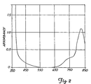
- Figure 2 shows the electromagnetic radiation absorbance characteristic of a typical photoconductor layer formed of the kinds of materials just described. As can be seen, the absorbance is relatively low in the visible portion of the electromagnetic radiation spectrum, and relatively high in the near infrared portion of that spectrum. The absorbance is also very high in the ultraviolet portion of the spectrum so that, clearly, ultraviolet radiation will not penetrate very far into photoconductor layer 16.
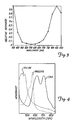
- Figure 3 shows the photoconductive response on a relative basis of a typical photoconductive layer formed of these materials. Clearly, substantial absorbance in a photoconductor layer formed of these materials also leads to a substantial photoconductive response in the material of photoconductor layer 16.
- the circumference of the cylindrical surface of drum 10 having this photoconductor layer therein has been selected to be 846.667 mm in this example.
- a typical surface velocity of the exposed surface of drum 10 during a reproduction cycle would be 5 mm/sec.
- Stepper motor 11 has been chosen in this example to provide 200,000 steps per a complete revolution of drum 10.
- organic photoconductor layer 16 is charged to a surface potential at its exposed surface of from typically 200 V to 450 V with respect to ground. Selected portions of that surface are thereafter discharged by a modulated, scanning laser beam to a lower potential at those locations encountering sufficient beam intensity under the modulation signal to result in forming a desired electrostatic charge pattern, or potential pattern, on that surface.
- This pattern is provided in accord with a color separation signal underlying the modulation signal which specifies the desired locations of a constituent color in a desired resulting printed image which is typically formed of three or four such colors, although there may be more colors used to achieve certain desired effects.
- the discharged areas remaining in layer 16 are then allowed to attract a selected toner having a desired constituent color, this attracted toner subsequently being transferred from the surface of drum 10 along with other color toners to the surface of the medium on which the printing is to occur to form a printed image.
- an electrifier, 17, such as a grid-controlled direct current corona discharge unit or scorotron, supplies, quite uniformly, a positive electric charge to adjacent portions of the outer surface portion of photoconductor layer 16 as they pass thereby during rotation of drum 10 which causes the surface past electrifier 17 to reach the desired initial surface potential, which is in the range indicated above, prior to its reaching the region of intersection with the scanning laser beam.
- the scanning laser beam modulated effectively by a corresponding color separation signal to provide the associated electric charge pattern on the outer surface of photoconductor layer 16 by selectively discharging that surface, does so successively for each of toner units 19.
- a toning developer arrangement, 18, contains six identical units, 19, each containing an alternative one of the four constituent color liquid toners that might each be used to form a corresponding subimage in route to forming a complete color printed image, plus two other alternative colored toners which may also be used for any special effects desired.
- the four colors typically are black, cyan, magenta and yellow liquid toners.
- Portions of the electromagnetic radiation absorbance characteristics for the cyan, magenta and yellow liquid toners used typically in the system of Figure 1 are shown in Figure 4. As can be seen there, the absorbance of electromagnetic radiation in the near infrared region of the spectrum, and for wavelengths beyond, is quite low for these toners.
- the scanning laser beam mentioned above is chosen to have its wavelength distribution to be primarily in the near infrared region of the spectrum so that this beam can pass through any toner which is on the outer surface of photoconductor layer 16 to discharge this layer below that portion of that surface impinged upon by the beam despite the presence of one or more toners thereon.
- each unit 19 there are pumping means to supply the toner to the surface of a moving band, 20, provided in each, this band being capable of being rotated across the outer surface of drum 10 parallel to the rotation axis thereof.
- a selected toner unit 19 has its band 20 charged to a voltage sufficiently above the discharge potential in laser beam exposed portions of photoconductor layer 16 to ensure adequate density of deposited toner in these laser exposed areas, but sufficiently below the initial charging potential of layer 16 to avoid unwanted toner deposits in the non-exposed regions.
- a vacuum provision arrangement is provided in each toner unit 19 on the side of the band opposite the pump means to remove excess liquid toner.
- a motor arrangement, 21, is controlled by control unit 12 to position a selected one of toner units 19 so that a surface of the band 20 therein is typically brought to within a few hundred microns of photoconductor layer 16 on drum 10 to thereby permit constituents of the toner in that unit to be attracted to corresponding portions of this outer surface of photoconductor layer 16.
- the selective impingement of the scanning laser beam with sufficient intensity at selected locations on the outer surface of photoconductor layer 16 results in a pattern of high and low surface potentials on this outer surface of layer 16 which can be developed into a visible image by the attraction of charged liquid toner selectively thereto, as described above.
- the potential value on band 20 is controlled so that positively charged, colored toner particles travel to only the portions of the outer surface of photoconductor layer 16 which have had the laser beam impinge thereon with sufficient intensity to discharge those portions to a surface potential, typically 40 to 70 V, which is well below that of the remaining portions of that outer surface which were typically initially charged by electrifier 17 to values in the range of 200 to 450 V.
- the electric field within the gap between the surface of photoconductor layer 16 and the band 20 induces disassociation of the toner material into its positively charged, colored particles and negatively charged, colorless counter-ions.
- an initial pattern of high and low surface potentials is established on the outer surface of photoconductor layer 16 followed by a corresponding toner deposition step, and then a new such pattern is provided on photoconductor layer 16 under the previous toner, or toners, each time there is a completion of the deposition of the toner for the previous charge pattern until the final toner to be used has been deposited on the outer surface of layer 16.
- Each of the corresponding toners attracted to its corresponding charge pattern is deposited as a subimage and accumulated on the outer surface of photoconductor layer 16 to form the complete toner image.
- Each of the subimages must be kept sufficiently well registered with respect to the others to obtain a clear, complete toner image.
- This complete toner image is subsequently transferred onto an intermediate medium formed by a coated polyester web, 22, which coating contains a thermally sensitive adhesive layer and a release/protective layer.
- Web 22 is shown in Figure 1 forced against layer 16 on drum 10 by a heated roller, 23, which results in a transfer of accumulated toner on photoconductor layer 16 to web 22 through being picked up by the adhesive layer therein.
- a later step results in transferring the accumulated toner, the adhesive layer and parts of the release/protective layer from web 22 onto the medium on which printing is to occur, such as paper, to thereby provide a halftone printing result using up to six colors.
- a laser electromagnetic radiation source arrangement 24, which is under the direction of control unit 12, to selectively discharge the outer surface of photoconductor layer 16 in drum 10.
- This beam is modulated by control unit 12 using such corresponding color separation signals as are obtained from a memory, 25.
- Laser beam source 24 correspondingly supplies the modulated laser beam, 26, having a nominal wavelength of 833 nm (near infrared) through an optical beam conditioning unit, 27, to impinge on an eight-faceted, rotating polygon mirror arrangement, 28, which is rotated by a motor, 29, again operated by control unit 12.
- Laser beam 26 is reflected from successive facets of rotating polygon 28 to then pass through further processing optics, 30, so as to repeatedly scan from left to right across the portion of the cylindrical surface of photoconductor layer 16 and drum 10 that is rotated thereunder.
- the electrostatic image established by the scanning laser beam for one toner must be "erased” before a subsequent electrostatic image can be formed for the following toner that is substantially free of any interfering effects lingering from the previous electrostatic image.
- any permanent changes in the material of photoconductor layer 16 must be avoided so that vestiges of one complete toner image do not appear in any subsequent complete toner image. Further, these effects must be overcome without an undue delay between the finishing of one complete toner image and the next.
- EP-A-0271334 which forms the preamble of the subject independent claims discloses an image forming method where a latent image is formed by subjecting an image retainer having a photoconductive layer to an image exposure, toner images formed by developing the latent image with a toner and wherein the step of forming the latent image and the step of forming the toner image are repeated at least once, and the plurality of toner images formed on the image retainer is transferred to a transfer material.
- This reference teaches that erasure radiation is absorbed by the charge generating material which is fundamentally different from the concept employed by the subject invention.
- the present invention provides for an electrostatic image removal system which can repeatably set surface potentials on an outer surface of a photoconductor layer in a drum rotatable about an axis before and after a discharge electromagnetic radiation beam provides an electrostatic image on the photoconductor layer outer surface for each of the toners used in providing a complete toner image on that outer surface.
- This outer surface is charged substantially uniformly as the drum rotates with a discharge electromagnetic radiation beam directed onto the photoconductor layer outer surface as charged to thereby discharge that surface at selected locations.
- a first toner is provided at the photoconductor layer outer surface with portions of it remaining at locations determined by the discharge electromagnetic radiation beam.
- First erasure electromagnetic radiation is provided on the photoconductor layer outer surface at locations free of the first toner and at locations where the first toner is present, as the first toner is capable of transmitting therethrough a substantial portion of the first erasure electromagnetic radiation.
- the first toner being on the surface of photoconductor layer, and perhaps other toners provided thereon in the same manner as the first toner, are then transferred substantially to a transfer means from the photoconductor layer outer surface.
- Termination erasure electromagnetic radiation is then directed onto the outer surface of the photoconductor layer, the termination erasure electromagnetic radiation having wavelengths in a termination spectral distribution which are shorter than those in the spectral distribution of the first erasure electromagnetic radiation.
- FIG. 1 shows a system in which the present invention is to be employed
- Image discharge means 32 is formed of a series of light-emitting diodes positioned along a line substantially parallel to the axis of rotation of drum 10 and separated by about 10 mm from the outer surface of photoconductor layer 16.
- the light-emitting diodes in image discharge means 32 emit electromagnetic radiation more or less centered about a wavelength of 840 nm, which is in the near infrared and substantially outside the strong absorption portions of the absorption characteristics of cyan, magenta and yellow toners as shown in Figure 4.
- This same light-emitting diode wavelength is sufficiently close to the near infrared absorption peak of photoconductive layer 16 as shown in Figure 2 to assure efficient discharging of the outer surface thereof to cause that surface potential to drop to between 0 and 40 V with respect to ground.
- this wavelength is also close to that of the radiation in laser beam 26 in laser arrangement 24 which also must efficiently discharge selected portions of photoconductor layer 16 to provide an electrostatic image therein.
- Image discharge means 32 could also be formed from light sources having a broader distribution of wavelengths than do light-emitting diodes so long as they provide a substantial part of their output energy in the near infrared region being considered here.
- a different unit 19 with a different colored toner has its band 20 brought to the immediate vicinity of the outer surface of photoconductor layer 16 by motor 21 under the direction of control unit 12 so that the positively charged toner particles are attracted to those portions of the surface of layer 16 (or to the surface of the first toner particles already thereon) which portions have been discharged by sufficient energy from beam 26 having been previously provided there by laser arrangement 24.
- the negatively charged colorless parts in the toner liquid are attracted to the other portions of the outer surface of layer 16 (or to the surface of the first toner particles already there).
- image discharge means 32 with its light emitting diodes discharges layer 16 by directing infrared energy thereon, including on those portions under the first and second toners or both, so that the surface potential thereof drops to a voltage in the range of 0 to 40 V.
- Cycle discharge means 33 is a source of electromagnetic radiation having wavelengths in the near ultraviolet portion of the electromagnetic spectrum with its peak wavelength at approximately 360 nm, this radiation being on the opposite side of the visible spectrum from the infrared radiation supplied by laser arrangement 24 and by image discharge means 32.
- This more energetic electromagnetic radiation from cycle discharge means 33 penetrates very little below the outer surface of photoconductor layer 16 because of its being so strongly absorbed by that layer as shown by the absorbance characteristic of that layer in Figure 2. Further, since the photoconductive response is also relatively high, i.e.
- Cycle discharge means 33 is positioned so that the ultraviolet lamp therein is approximately 1.0 cm from the outer surface of photoconductor layer 16, and this exposure occurs through a slit aperature parallel to the rotation axis of drum 10 which extends across the entirety of layer 16 and provides a 5.0 mm wide opening.
- the ultraviolet radiation passes through this opening and an optional neutral density filter to substantially uniformly provide ultraviolet radiation of 0.05 to 2.0 mW/cm on the portion of the outer surface of layer 16 illuminated thereby. This value is chosen to neutralize the bulk trapped charges while avoiding excess exposure which would lead to generation of too many hole carriers with relatively long lifetimes which has the consequence of prolonging the dark adaptation period of photoconductor layer 16 necessary for eliminating such excess hole carriers.
- the intensities chosen for the radiation provided by both image discharge means 32 and cycle discharge means 33 are dependent on the type of material used in photoconductor layer 16, the rotation speed of drum 10, the separations between these radiation sources and the outer surface of layer 16, the extent of the effective apertures used therewith in controlling the geometrical extent of the portion of the surface of layer 16 illuminated thereby, and the like. Thus, some adjustment in the intensities used, or the apertures, or other variables is usually needed to adapt the sources for proper operation in a particular system of the type in Figure 1.
- the provision of the ultraviolet radiation on the outer surface of photoconductor layer 16 to neutralize bulk trapped charges affects the dark condition surface potential decay rate. This results in a subsequent decrease in surface potential after a subsequent charging of the outer surface of photoconductor layer 16 by electrifier 17 in beginning another formation of a complete toner image even though the charging conditions using electrifier 17 remain unchanged.
- a probable reason for this is the fact that the ultraviolet radiation in generating mobile hole charge carriers continues to do so until terminated so that some mobile hole carriers will leave behind unneutralized trapped negative charges. These trapped negative charges again effectively reduce the surface potential, and this effect can persist for several minutes after the termination of the impingement of ultraviolet radiation on the outer surface of layer 16. In these circumstances, the operator is either forced to wait for a substantial amount of time before beginning formation of a subsequent toner image, or some further step must be taken to ready photoconductor layer 16 to reduce such a waiting time.
- One method for reducing such a waiting period is to operate electrifier 17 once again following the transfer of a complete toner image before beginning the formation of a subsequent complete toner image.
- Electrifier 17 then deposits positive charge on the outer surface of photoconductor layer 16 to raise its surface potential to a relatively low value, typically 100 V, immediately after operation of cycle discharge means 33.
- the effect of such an application of positive charge to the outer surface of photoconductor layer 16 is to sweep the excess positive charges, or mobile hole charges, from the layer before charging that surface to the desired initial potential in the formation of the first toner subimage as part of providing the next printed image.
Landscapes
- Physics & Mathematics (AREA)
- General Physics & Mathematics (AREA)
- Health & Medical Sciences (AREA)
- Toxicology (AREA)
- Color Electrophotography (AREA)
- Discharging, Photosensitive Material Shape In Electrophotography (AREA)
- Electrostatic Charge, Transfer And Separation In Electrography (AREA)
- Combination Of More Than One Step In Electrophotography (AREA)
Claims (12)
- Verfahren zum mehrfachen elektrischen Laden einer Photoleiterschicht auf einem elektrischen Leiter, der mindestens als ein Teil des Äußeren einer Trommel vorgesehen ist, so daß wenigstens Teilstücke einer Außenoberfläche der Photoleiterschicht nach jedem ausgewählten derartigen Ladevorgang auf ein ausgewähltes erstes Oberflächenpotential gebracht werden, wobei das Verfahren die folgenden Schritte umfaßt:Aufladen der Außenoberfläche (16) der Photoleiterschicht auf das erste Oberflächenpotential, und zwar durch im wesentlichen gleichmäßiges Auftragen der elektrischen Ladung über mindestens einen Teil der Oberfläche, während sich die Trommel um eine Rotationsachse der Trommel dreht;Richten eines Entladungsstrahls elektromagnetischer Strahlung (24-30) auf eine erste Gruppe von ausgewählten Positionen auf der Außenoberfläche (16) der Photoleiterschicht, die vorher aufgeladen worden ist, wobei die Intensität des Strahls ausreichend ist, um dadurch Teilstücke der Photoleiterschicht neben der ersten Gruppe ausgewählter Positionen zu entladen;Bereitstellung eines ersten Toners (19-21) an der Außenoberfläche (16) der Photoleiterschicht, wobei Teilstücke des ersten Toners an Positionen auf der Außenoberfläche der Photoleiterschicht verbleiben, die dadurch bestimmt werden, welche Teilstücke der Photoleiterschicht durch den Entladungsstrahl elektromagnetischer Strahlung entladen worden sind;Bereitstellung einer ersten elektromagnetischen Löschstrahlung (32) auf der Außenoberfläche (16) der Photoleiterschicht, und zwar sowohl an Positionen, an denen sich der erste Toner nicht befindet sowie an Positionen, an denen der erste Toner vorhanden ist, wobei der erste Toner einen großen Teil der ersten elektromagnetischen Löschstrahlung hindurchlassen kann, wobei die erste elektromagnetische Löschstrahlung Wellenlängen im nahen Infrarotspektrum aufweist und im wesentlichen außerhalb der Abschnitte mit starker Absorption der Absorptionseigenschaften Cyan, Magenta und Gelb; undÜbertragung im wesentlichen aller Teile des ersten Toners von der Außenoberfläche der Photoleiterschicht auf eine Übertragungseinrichtung (22);gekennzeichnet durch die Bereitstellung einer energetischen elektromagnetischen Terminationsstrahlung (von 33) auf der Außenoberfläche der Photoleiterschicht mit Wellenlängen in einer spektralen Terminationsverteilung im wesentlichen im nahen Ultraviolettbereich,wobei sowohl die erste Strahlung als auch die Terminationsstrahlung von der Photoleiterschicht absorbiert werden.
- Verfahren nach Anspruch 1, wobei die energetische elektromagnetische Terminationsstrahlung sehr geringfügig unter die Außenoberfläche der Photoleiterschicht (16) dringt, da sie sehr stark absorbiert wird.
- Verfahren nach Anspruch 1, wobei auf die Bereitstellung der ersten elektromagnetischen Löschstrahlung die folgenden Schritten folgen:erneutes Aufladen der Außenoberfläche der Photoleiterschicht auf das erste Oberflächenpotential, und zwar durch im wesentlichen gleichmäßiges Auftragen der elektrischen Ladung über mindestens einen Teil der Oberfläche, während sich die Trommel um eine Rotationsachse der Trommel dreht;Richten eines Entladungsstrahls elektromagnetischer Strahlung (24-30) auf eine zweite Gruppe von ausgewählten Positionen auf der Außenoberfläche (16) der Photoleiterschicht, die vorher zuletzt aufgeladen worden ist, wobei die Intensität des Strahls ausreichend ist, um dadurch Teilstücke der Photoleiterschicht neben der zweiten Gruppe ausgewählter Positionen zu entladen;Bereitstellung eines zweiten Toners (19-21) an der Außenoberfläche der Photoleiterschicht, wobei Teilstücke des zweiten Toners an Positionen auf der Außenoberfläche der Photoleiterschicht verbleiben, die dadurch bestimmt werden, welche Teilstücke der Photoleiterschicht durch den Entladungsstrahl elektromagnetischer Strahlung entladen worden sind; undÜbertragung im wesentlichen aller Teile des ersten und zweiten Toners von der Außenoberfläche der Photoleiterschicht auf eine Übertragungseinrichtung (22);
- Verfahren nach Anspruch 3, wobei auf die Bereitstellung eines zweiten Toners der folgende Schritt folgt:
Bereitstellung einer zweiten elektromagnetischen Löschstrahlung (32) auf der Außenoberfläche (16) der Photoleiterschicht, und zwar sowohl an Positionen, an denen sich der erste und der zweite Toner nicht befinden sowie an Positionen, an denen entweder der erste oder der zweite Toner vorhanden ist, wobei der erste und der zweite Toner einen großen Teil der zweiten elektromagnetischen Löschstrahlung hindurchlassen kann, wobei die zweite elektromagnetische Löschstrahlung (32) Wellenlängen in einer zweiten spektralen Verteilung auweist, wobei die Wellenlängen allgemein länger sind als die Wellenlängen in der spektralen Terminationsverteilung (31). - Verfahren nach Anspruch 1, wobei auf die Bereitstellung der elektromagnetischen Terminationsstrahlung (33) der folgende Schritt folgt:
Aufladen (17) der Außenoberfläche der Photoleiterschicht auf ein Terminations-Oberflächenpotential, das kleiner ist als das erste Oberflächenpotential, durch im wesentlichen gleichmäßiges Auftragen elektrischer Ladung über wenigstens ein Teilstück der Außenoberfläche der Photoleiterschicht, während sich die Trommel um ihre Rotationsachse dreht. - Verfahren nach Anspruch 4, wobei auf die Bereitstellung der zweiten elektromagnetischen Löschstrahlung die folgenden Schritte folgen:erneutes Aufladen der Außenoberfläche (16) der Photoleiterschicht auf das erste Oberflächenpotential, und zwar durch im wesentlichen gleichmäßiges Auftragen der elektrischen Ladung über mindestens einen Teil der Oberfläche, während sich die Trommel um eine Rotationsachse der Trommel dreht;Richten eines Entladungsstrahls elektromagnetischer Strahlung (24-30) auf eine dritte Gruppe von ausgewählten Positionen auf der Außenoberfläche der Photoleiterschicht, die vorher zuletzt aufgeladen worden ist, wobei die Intensität des Strahls ausreichend ist, um dadurch Teilstücke der Photoleiterschicht neben der dritten Gruppe ausgewählter Positionen zu entladen;Bereitstellung eines dritten Toners (19-21) auf der Außenoberfläche der Photoleiterschicht, wobei Teilstücke des dritten Toners an Positionen auf der Außenoberfläche der Photoleiterschicht verbleiben, die dadurch bestimmt werden, welche Teilstücke der Photoleiterschicht durch den Entladungsstrahl elektromagnetischer Strahlung entladen worden sind; undÜbertragung im wesentlichen aller Teile des ersten, zweiten und dritten Toners von der Außenoberfläche der Photoleiterschicht auf die Übertragungseinrichtung (22);
- Verfahren nach Anspruch 6, wobei auf die Bereitstellung eines dritten Toners der folgende Schritt folgt:
Bereitstellung einer dritten elektromagnetischen Löschstrahlung (32) auf der Außenoberfläche der Photoleiterschicht, und zwar sowohl an Positionen, an denen sich der erste, zweite und dritte Toner nicht befinden sowie an Positionen, an denen entweder der erste, zweite oder dritte Toner vorhanden ist, wobei der erste, zweite und dritte Toner einen großen Teil der dritten elektromagnetischen Löschstrahlung hindurchlassen können, wobei die dritte elektromagnetische Löschstrahlung (32) Wellenlängen in einer dritten spektralen Verteilung auweist, wobei die Wellenlängen im wesentlichen länger sind als die Wellenlängen in der spektralen Terminationsverteilung. - Verfahren nach Anspruch 7, wobei auf die Bereitstellung der dritten elektromagnetischen Löschstrahlung die folgenden Schritte folgen:erneutes Aufladen der Außenoberfläche der Photoleiterschicht auf das erste Oberflächenpotential, und zwar durch im wesentlichen gleichmäßiges Auftragen der elektrischen Ladung über mindestens einen Teil der Oberfläche, während sich die Trommel um eine Rotationsachse der Trommel dreht;Richten eines Entladungsstrahls elektromagnetischer Strahlung (24-30) auf eine vierte Gruppe von ausgewählten Positionen auf der Außenoberfläche (16) der Photoleiterschicht, die vorher zuletzt aufgeladen worden ist, wobei die Intensität des Strahls ausreichend ist, um dadurch Teilstücke der Photoleiterschicht neben der vierten Gruppe ausgewählter Positionen zu entladen;Bereitstellung eines vierten Toners (19-21) auf der Außenoberfläche der Photoleiterschicht, wobei Teilstücke des vierten Toners an Positionen auf der Außenoberfläche der Photoleiterschicht verbleiben, die dadurch bestimmt werden, welche Teilstücke der Photoleiterschicht durch den Entladungsstrahl elektromagnetischer Strahlung entladen worden sind; undÜbertragung im wesentlichen aller Teile des ersten, zweiten, dritten und vierten Toners von der Außenoberfläche der Photoleiterschicht auf die Übertragungseinrichtung (22);
- Verfahren nach Anspruch 8, wobei auf die Bereitstellung eines vierten Toners der folgende Schritt folgt:
Bereitstellung einer vierten elektromagnetischen Löschstrahlung (32) auf der Außenoberfläche der Photoleiterschicht, und zwar sowohl an Positionen, an denen sich der erste, zweite, dritte und vierte Toner nicht befinden sowie an Positionen, an denen entweder der erste, zweite, dritte oder vierte Toner vorhanden ist, wobei der erste, zweite, dritte und vierte Toner einen großen Teil der vierten elektromagnetischen Löschstrahlung hindurchlassen können, wobei die vierte elektromagnetische Löschstrahlung Wellenlängen in einer vierten spektralen Verteilung aufweist, wobei die Wellenlängen im wesentlichen länger sind als die Wellenlängen in der spektralen Terminationsverteilung. - Verfahren nach Anspruch 1, wobei der Entladungsstrahl elektromagnetischer Strahlung eine Wellenlänge aufweist, die sich im Bereich der ersten elektromagnetischen Löschstrahlung befindet.
- Vorrichtung zum mehrfachen elektrischen Laden einer Photoleiterschicht (16) auf einem elektrischen Leiter, der mindestens als ein Teil des Äußeren einer Trommel (10) vorgesehen ist, so daß wenigstens Teilstücke einer Außenoberfläche der Photoleiterschicht nach jedem ausgewählten derartigen Ladevorgang auf ein ausgewähltes erstes Oberflächenpotential gebracht werden, wobei die Vorrichtung folgendes umfaßt:eine Ladeeinrichtung zum Aufladen der Außenoberfläche (16) der Photoleiterschicht auf das erste Oberflächenpotential, und zwar durch im wesentlichen gleichmäßiges Auftragen der elektrischen Ladung über mindestens einen Teil der Oberfläche, während sich die Trommel (10) um eine Rotationsachse der Trommel dreht;selektive Entladungseinrichtungen (24-30) zum Richten eines Entladungsstrahls elektromagnetischer Strahlung (26) auf ausgewählte Gruppen ausgewählter Positionen auf der Außenoberfläche der Photoleiterschicht, die vorher aufgeladen worden ist, wobei die Intensität des Strahls ausreichend ist, um dadurch Teilstücke der Photoleiterschicht neben den ausgewählten Gruppen ausgewählter Positionen zu entladen;eine Toner-Bereitstellungseinrichtung (19-21) zur Bereitstellung ausgewählter, verschiedener Toner auf der Außenoberfläche der Photoleiterschicht, wobei Teilstücke dieser ausgewählten Toner an Positionen auf der Außenoberfläche der Photoleiterschicht verbleiben, die dadurch bestimmt werden, welche Teilstücke der Photoleiterschicht entsprechend durch den Entladungsstrahl elektromagnetischer Strahlung entladen worden sind;eine erste Löscheinrichtung (32) zur Bereitstellung einer elektromagnetischen Löschstrahlung auf der Außenoberfläche der Photoleiterschicht, und zwar sowohl an Positionen, an denen sich kein Toner befindet sowie an Positionen, an denen mindestens einer der Toner vorhanden ist, wobei diese Toner einen großen Teil der elektromagnetischen Löschstrahlung hindurchlassen können, wobei die elektromagnetische Löschstrahlung Wellenlängen im nahen Infrarotspektrum aufweist und im wesentlichen außerhalb des Abschnitts mit starker Absorption der Absorptionseigenschaften Cyan, Magenta und Gelb; undeine Übertragungseinrichtung (23), die im wesentlichen alle Teile der Toner, die auf der Außenoberfläche der Photoleiterschicht verbleiben, auf eine Übertragungseinrichtung (22) übertragen können;gekennzeichnet durch eine Terminations-Löscheinrichtung (33), die so angeordnet ist, daß sie eine energetische elektromagnetische Terminationsstrahlung auf der Außenoberfläche der Photoleiterschicht vorsieht, und zwar mit Wellenlängen in einer spektralen Terminationsverteilung im wesentlichen im nahen Ultraviolettbereich,wobei sowohl die erste Strahlung als auch die Terminationsstrahlung von der Photoleiterschicht absorbiert werden.
- Vorrichtung nach Anspruch 11, wobei ferner eine eine Terminations-Ladeeinrichtung (17) vorgesehen ist, die die Außenoberfläche (16) der Photoleiterschicht auf ein Terminations-Oberflächenpotential aufladen kann, nachdem die elektromagnetische Terminationsstrahlung durch im wesentlichen gleichmäßiges Auftragen elektrischer Ladung auf mindestens einem Teilstück der Außenoberfläche der Photoleiterschicht auf der Oberfläche aufgetragen worden ist, während sich die Trommel (10) um ihre Rotationsachse dreht, wobei das Terminationsoberflächenpotential kleiner ist als das erste Oberflächenpotential.
Applications Claiming Priority (2)
| Application Number | Priority Date | Filing Date | Title |
|---|---|---|---|
| US07/552,698 US5083163A (en) | 1990-07-16 | 1990-07-16 | Photoconductor resetting following multiple charge images |
| US552698 | 1995-11-03 |
Publications (3)
| Publication Number | Publication Date |
|---|---|
| EP0467609A2 EP0467609A2 (de) | 1992-01-22 |
| EP0467609A3 EP0467609A3 (de) | 1992-12-30 |
| EP0467609B1 true EP0467609B1 (de) | 1996-02-21 |
Family
ID=24206416
Family Applications (1)
| Application Number | Title | Priority Date | Filing Date |
|---|---|---|---|
| EP91306367A Expired - Lifetime EP0467609B1 (de) | 1990-07-16 | 1991-07-15 | Verfahren und Gerät zum mehrfachen elektrischen Laden einer Photoleiterschicht |
Country Status (5)
| Country | Link |
|---|---|
| US (1) | US5083163A (de) |
| EP (1) | EP0467609B1 (de) |
| JP (1) | JPH04234068A (de) |
| KR (1) | KR930002892A (de) |
| DE (1) | DE69117224T2 (de) |
Cited By (1)
| Publication number | Priority date | Publication date | Assignee | Title |
|---|---|---|---|---|
| US6836630B2 (en) | 2002-09-23 | 2004-12-28 | Hewlett-Packard Development Company, L.P. | Reduction of wear on selected components in multi-color imaging apparatus |
Families Citing this family (7)
| Publication number | Priority date | Publication date | Assignee | Title |
|---|---|---|---|---|
| US5534980A (en) * | 1994-05-31 | 1996-07-09 | Mita Industrial Co., Ltd. | Electrophotographic image forming apparatus having a charge removing means |
| US5510626A (en) * | 1994-06-22 | 1996-04-23 | Minnesota Mining And Manufacturing Company | System and method for conditioning a radiation detector |
| US5606398A (en) * | 1995-04-28 | 1997-02-25 | Minnesota Mining And Manufacturing Company | Reduction of residual potential and ghosting in a photoconductor |
| EP0852748A1 (de) * | 1995-09-29 | 1998-07-15 | Imation Corp. | Verfahren und apparat zur herstellung eines vielfarbenbildes in einem elektrofotographischen system |
| US5650253A (en) * | 1995-09-29 | 1997-07-22 | Minnesota Mining And Manufacturing Company | Method and apparatus having improved image transfer characteristics for producing an image on a receptor medium such as a plain paper |
| US5725980A (en) * | 1997-01-21 | 1998-03-10 | Xerox Corporation | Multi-wavelength laser which avoids excessive light absorption by cyan pigment in image-on-image electrophotography |
| DE10353029B3 (de) * | 2003-11-13 | 2004-08-19 | Heidelberger Druckmaschinen Ag | Vorrichtung und Verfahren zur Messung der Längenänderung der Vorschubspindel in einem Belichter für Druckvorlagen |
Family Cites Families (22)
| Publication number | Priority date | Publication date | Assignee | Title |
|---|---|---|---|---|
| US4035750A (en) * | 1975-10-14 | 1977-07-12 | Eastman Kodak Company | Electrophotographic apparatus having improved photoconductor regenerative structure and procedure |
| DE2635731C2 (de) * | 1976-08-09 | 1982-06-24 | Siemens AG, 1000 Berlin und 8000 München | Vorrichtung für ein Elektrofotografisches Verfahren |
| US4340656A (en) * | 1978-04-07 | 1982-07-20 | Minolta Camera Kabushiki Kaisha | Electrophotographic copying method with residual charge erasing step |
| US4286032A (en) * | 1978-04-27 | 1981-08-25 | Canon Kabushiki Kaisha | Electrophotographic process and apparatus therefor |
| US4367274A (en) * | 1981-02-23 | 1983-01-04 | Minnesota Mining And Manufacturing Company | Sensitized organic electron donor bis-benzocarbazole compounds |
| US4361637A (en) * | 1981-02-23 | 1982-11-30 | Minnesota Mining And Manufacturing Company | Electron bis-benzocarbazole donor compounds and photoconductive charge transport materials |
| US4357405A (en) * | 1981-02-23 | 1982-11-02 | Minnesota Mining And Manufacturing Company | Fluorinated dye sensitized organic electron donor compound |
| US4337305A (en) * | 1981-02-23 | 1982-06-29 | Minnesota Mining And Manufacturing Company | Sensitized organic electron donor compounds |
| US4356244A (en) * | 1981-02-23 | 1982-10-26 | Minnesota Mining And Manufacturing Company | Quinoxaline cyanine dye sensitized organic electron donor compounds |
| JPS5823033A (ja) * | 1981-08-03 | 1983-02-10 | Fuji Xerox Co Ltd | 電子写真法 |
| US4408865A (en) * | 1981-11-23 | 1983-10-11 | Hewlett Packard Company | Corona discharge device for electrophotographic charging and potential leveling |
| DE3377023D1 (en) * | 1982-07-29 | 1988-07-14 | Minnesota Mining & Mfg | Triarylmethane compounds, their preparation and use as photoconductive systems |
| JPS59155879A (ja) * | 1983-02-25 | 1984-09-05 | Fuji Xerox Co Ltd | 静電荷除去装置 |
| US4538900A (en) * | 1983-11-09 | 1985-09-03 | Ricoh Company, Ltd. | Electrophotographic copying apparatus including drum conditioning apparatus and method |
| EP0154042B1 (de) * | 1984-02-28 | 1988-05-04 | Agfa-Gevaert N.V. | Herstellung von entwickelten elektrostatischen Bildern |
| DE3536836A1 (de) * | 1984-10-17 | 1986-04-17 | Sharp K.K., Osaka | Entladevorrichtung fuer ein kopiergeraet |
| US4804602A (en) * | 1986-03-12 | 1989-02-14 | Eastman Kodak Company | Method and apparatus utilizing corona erase for improving a multi-color electrophotographic image |
| JPS62238585A (ja) * | 1986-04-09 | 1987-10-19 | Asahi Optical Co Ltd | 電子写真法による多色画像形成方法 |
| US4897330A (en) * | 1986-12-09 | 1990-01-30 | Konica Corporation | Image forming method |
| US4728983A (en) * | 1987-04-15 | 1988-03-01 | Minnesota Mining And Manufacturing Company | Single beam full color electrophotography |
| GB8712151D0 (en) * | 1987-05-22 | 1987-06-24 | Minnesota Mining & Mfg | Dyes |
| JPS63303365A (ja) * | 1987-06-03 | 1988-12-09 | Minolta Camera Co Ltd | 画像編集方法 |
-
1990
- 1990-07-16 US US07/552,698 patent/US5083163A/en not_active Expired - Fee Related
-
1991
- 1991-07-15 EP EP91306367A patent/EP0467609B1/de not_active Expired - Lifetime
- 1991-07-15 KR KR1019910012033A patent/KR930002892A/ko not_active Withdrawn
- 1991-07-15 DE DE69117224T patent/DE69117224T2/de not_active Expired - Fee Related
- 1991-07-16 JP JP3175052A patent/JPH04234068A/ja active Pending
Cited By (1)
| Publication number | Priority date | Publication date | Assignee | Title |
|---|---|---|---|---|
| US6836630B2 (en) | 2002-09-23 | 2004-12-28 | Hewlett-Packard Development Company, L.P. | Reduction of wear on selected components in multi-color imaging apparatus |
Also Published As
| Publication number | Publication date |
|---|---|
| KR930002892A (ko) | 1993-02-23 |
| DE69117224T2 (de) | 1996-10-02 |
| DE69117224D1 (de) | 1996-03-28 |
| EP0467609A3 (de) | 1992-12-30 |
| EP0467609A2 (de) | 1992-01-22 |
| US5083163A (en) | 1992-01-21 |
| JPH04234068A (ja) | 1992-08-21 |
Similar Documents
| Publication | Publication Date | Title |
|---|---|---|
| US5166734A (en) | Imaging system including pre-transfer discharge | |
| US4761669A (en) | Highlight color printing | |
| EP0028680B1 (de) | Verfahren und Vorrichtung zum Aufladen eines Bildelements in einer elektrophotographischen Maschine | |
| JP3456666B2 (ja) | 二重波長単一光学系ros及び二重層感光体を備えたフルカラー・ゼログラフィック印刷システム | |
| US4230783A (en) | Process and apparatus for electrophotography | |
| US5083163A (en) | Photoconductor resetting following multiple charge images | |
| EP0715224B1 (de) | Verfahren und Vorrichtung zur Erzeugung von mehreren Bildern | |
| US5576824A (en) | Five cycle image on image printing architecture | |
| EP0314457B1 (de) | Verfahren und Vorrichtung für die Farbelektrophotographie | |
| US5038177A (en) | Selective pre-transfer corona transfer with light treatment for tri-level xerography | |
| US4256820A (en) | Method of electrophotography using low intensity exposive | |
| JP3379803B2 (ja) | 2波長単一光学系ros及び2層形感光体を用いたカラーゼログラフィ印刷装置 | |
| EP0921443B1 (de) | Additive Wiederaufladung, Belichtung, und Entwicklung elektrophotographischer Farbdruck | |
| US5351113A (en) | Pre-pretransfer treatment to increase transfer latitude in tri-level xerography | |
| US4607934A (en) | Electrophotography using a photosensitive drum with multi-photosensitive layers sensitive to different wave lengths | |
| US4937636A (en) | Single pass, two-color electrophotographic reproduction machine | |
| EP0823075B1 (de) | Verringerung von restpotential und geisterbildformung in einem photoleiter | |
| JP4275758B2 (ja) | フルカラー画像生成方法 | |
| US4725867A (en) | Apparatus for forming a multi-color image on an electrophotographic element which is sensitive to light outside the visible spectrum | |
| CA1230915A (en) | Method and apparatus of electrophotography | |
| EP0361851B1 (de) | Photorezeptorrandlöschsystem, insbesondere für Dreistufenxerographie | |
| US4645330A (en) | Electrophotographic device | |
| US5247328A (en) | Method and apparatus for charging a photoconductive surface to a uniform potential | |
| US5978628A (en) | Highlight color read printing using additive toners | |
| US6208819B1 (en) | Method for discharging photoreceptor residual charges |
Legal Events
| Date | Code | Title | Description |
|---|---|---|---|
| PUAI | Public reference made under article 153(3) epc to a published international application that has entered the european phase |
Free format text: ORIGINAL CODE: 0009012 |
|
| AK | Designated contracting states |
Kind code of ref document: A2 Designated state(s): DE FR GB IT |
|
| PUAL | Search report despatched |
Free format text: ORIGINAL CODE: 0009013 |
|
| AK | Designated contracting states |
Kind code of ref document: A3 Designated state(s): DE FR GB IT |
|
| 17P | Request for examination filed |
Effective date: 19930527 |
|
| 17Q | First examination report despatched |
Effective date: 19940728 |
|
| GRAA | (expected) grant |
Free format text: ORIGINAL CODE: 0009210 |
|
| ITF | It: translation for a ep patent filed | ||
| AK | Designated contracting states |
Kind code of ref document: B1 Designated state(s): DE FR GB IT |
|
| REF | Corresponds to: |
Ref document number: 69117224 Country of ref document: DE Date of ref document: 19960328 |
|
| ET | Fr: translation filed | ||
| PLBE | No opposition filed within time limit |
Free format text: ORIGINAL CODE: 0009261 |
|
| STAA | Information on the status of an ep patent application or granted ep patent |
Free format text: STATUS: NO OPPOSITION FILED WITHIN TIME LIMIT |
|
| 26N | No opposition filed | ||
| PGFP | Annual fee paid to national office [announced via postgrant information from national office to epo] |
Ref country code: GB Payment date: 19980623 Year of fee payment: 8 |
|
| PGFP | Annual fee paid to national office [announced via postgrant information from national office to epo] |
Ref country code: FR Payment date: 19980707 Year of fee payment: 8 |
|
| PG25 | Lapsed in a contracting state [announced via postgrant information from national office to epo] |
Ref country code: GB Free format text: LAPSE BECAUSE OF NON-PAYMENT OF DUE FEES Effective date: 19990715 |
|
| PG25 | Lapsed in a contracting state [announced via postgrant information from national office to epo] |
Ref country code: FR Free format text: THE PATENT HAS BEEN ANNULLED BY A DECISION OF A NATIONAL AUTHORITY Effective date: 19990731 |
|
| GBPC | Gb: european patent ceased through non-payment of renewal fee |
Effective date: 19990715 |
|
| REG | Reference to a national code |
Ref country code: FR Ref legal event code: ST |
|
| PGFP | Annual fee paid to national office [announced via postgrant information from national office to epo] |
Ref country code: DE Payment date: 20000727 Year of fee payment: 10 |
|
| PG25 | Lapsed in a contracting state [announced via postgrant information from national office to epo] |
Ref country code: DE Free format text: LAPSE BECAUSE OF NON-PAYMENT OF DUE FEES Effective date: 20020501 |
|
| PG25 | Lapsed in a contracting state [announced via postgrant information from national office to epo] |
Ref country code: IT Free format text: LAPSE BECAUSE OF NON-PAYMENT OF DUE FEES;WARNING: LAPSES OF ITALIAN PATENTS WITH EFFECTIVE DATE BEFORE 2007 MAY HAVE OCCURRED AT ANY TIME BEFORE 2007. THE CORRECT EFFECTIVE DATE MAY BE DIFFERENT FROM THE ONE RECORDED. Effective date: 20050715 |