EP0468135A2 - Dynamischer wahlfreier Speicher mit hoher Geschwindigkeit und verlängerter Rückstell-/Vorladezeit - Google Patents
Dynamischer wahlfreier Speicher mit hoher Geschwindigkeit und verlängerter Rückstell-/Vorladezeit Download PDFInfo
- Publication number
- EP0468135A2 EP0468135A2 EP91104396A EP91104396A EP0468135A2 EP 0468135 A2 EP0468135 A2 EP 0468135A2 EP 91104396 A EP91104396 A EP 91104396A EP 91104396 A EP91104396 A EP 91104396A EP 0468135 A2 EP0468135 A2 EP 0468135A2
- Authority
- EP
- European Patent Office
- Prior art keywords
- row address
- dram
- level
- circuit
- active
- Prior art date
- Legal status (The legal status is an assumption and is not a legal conclusion. Google has not performed a legal analysis and makes no representation as to the accuracy of the status listed.)
- Granted
Links
Images


Classifications
-
- G—PHYSICS
- G11—INFORMATION STORAGE
- G11C—STATIC STORES
- G11C11/00—Digital stores characterised by the use of particular electric or magnetic storage elements; Storage elements therefor
- G11C11/21—Digital stores characterised by the use of particular electric or magnetic storage elements; Storage elements therefor using electric elements
- G11C11/34—Digital stores characterised by the use of particular electric or magnetic storage elements; Storage elements therefor using electric elements using semiconductor devices
- G11C11/40—Digital stores characterised by the use of particular electric or magnetic storage elements; Storage elements therefor using electric elements using semiconductor devices using transistors
- G11C11/401—Digital stores characterised by the use of particular electric or magnetic storage elements; Storage elements therefor using electric elements using semiconductor devices using transistors forming cells needing refreshing or charge regeneration, i.e. dynamic cells
- G11C11/4063—Auxiliary circuits, e.g. for addressing, decoding, driving, writing, sensing or timing
- G11C11/407—Auxiliary circuits, e.g. for addressing, decoding, driving, writing, sensing or timing for memory cells of the field-effect type
- G11C11/409—Read-write [R-W] circuits
- G11C11/4094—Bit-line management or control circuits
-
- G—PHYSICS
- G11—INFORMATION STORAGE
- G11C—STATIC STORES
- G11C11/00—Digital stores characterised by the use of particular electric or magnetic storage elements; Storage elements therefor
- G11C11/21—Digital stores characterised by the use of particular electric or magnetic storage elements; Storage elements therefor using electric elements
- G11C11/34—Digital stores characterised by the use of particular electric or magnetic storage elements; Storage elements therefor using electric elements using semiconductor devices
- G11C11/40—Digital stores characterised by the use of particular electric or magnetic storage elements; Storage elements therefor using electric elements using semiconductor devices using transistors
- G11C11/401—Digital stores characterised by the use of particular electric or magnetic storage elements; Storage elements therefor using electric elements using semiconductor devices using transistors forming cells needing refreshing or charge regeneration, i.e. dynamic cells
- G11C11/4063—Auxiliary circuits, e.g. for addressing, decoding, driving, writing, sensing or timing
- G11C11/407—Auxiliary circuits, e.g. for addressing, decoding, driving, writing, sensing or timing for memory cells of the field-effect type
- G11C11/4072—Circuits for initialization, powering up or down, clearing memory or presetting
-
- G—PHYSICS
- G11—INFORMATION STORAGE
- G11C—STATIC STORES
- G11C11/00—Digital stores characterised by the use of particular electric or magnetic storage elements; Storage elements therefor
- G11C11/21—Digital stores characterised by the use of particular electric or magnetic storage elements; Storage elements therefor using electric elements
- G11C11/34—Digital stores characterised by the use of particular electric or magnetic storage elements; Storage elements therefor using electric elements using semiconductor devices
- G11C11/40—Digital stores characterised by the use of particular electric or magnetic storage elements; Storage elements therefor using electric elements using semiconductor devices using transistors
- G11C11/401—Digital stores characterised by the use of particular electric or magnetic storage elements; Storage elements therefor using electric elements using semiconductor devices using transistors forming cells needing refreshing or charge regeneration, i.e. dynamic cells
- G11C11/4063—Auxiliary circuits, e.g. for addressing, decoding, driving, writing, sensing or timing
- G11C11/407—Auxiliary circuits, e.g. for addressing, decoding, driving, writing, sensing or timing for memory cells of the field-effect type
- G11C11/4076—Timing circuits
-
- G—PHYSICS
- G11—INFORMATION STORAGE
- G11C—STATIC STORES
- G11C8/00—Arrangements for selecting an address in a digital store
- G11C8/18—Address timing or clocking circuits; Address control signal generation or management, e.g. for row address strobe [RAS] or column address strobe [CAS] signals
Definitions
- This invention relates to dynamic random access semiconductor memories (DRAM) and, more particularly, to a system for increasing the available time for row reset/precharge time in a DRAM.
- DRAM dynamic random access semiconductor memories
- an address system in which row and column addresses are multiplexed through a set of address terminals in response to a pair of external clocks.
- the first clock generates a row address strobe (RAS) and a second clock generates a column address strobe (CAS).
- RAS row address strobe
- CAS column address strobe
- the RAS signal is active for a portion of the time and inactive for another portion of the time. During its active state, it is at a logical low level and during its inactive state, it is at a logical high level. When the RAS signal is in its inactive state, presetting and recharging of the DRAM circuitry is accomplished to ready it for the next memory cycle.
- word lines i.e., X address lines
- the active state low logical level
- the standby state high logical level
- an internal read-write cycle restores charges to memory cell storage capacitors; address buffers and sense amplifiers are reset; and bit lines are precharged.
- DRAMS have seen wide usage in personal computers (PC).
- PC personal computers
- a personal computer's clock is eight or ten mHz
- most DRAMS are fast enough to keep up with the PC's central processing unit (CPU). If the CPU clock runs faster, a conventional DRAM is unable to keep up with the CPU's clock rate and system performance is thereby degraded.
- each clock cycle is, at least, 100 nanoseconds long and there is more than sufficient time to perform the DRAM's reset/precharge functions.
- each CPU clock cycle is 30 nanoseconds and, a computer-generated RAS signal allows only approximately 20 nanoseconds for reset/precharge functions. This is inadequate for high speed DRAMS, which require a reset/precharge time of 30 nanoseconds.
- Sense-amplifiers are connected to the bit line pair.
- Static memory cells are also connected to the bit lines and serve as an auxiliary memory.
- the static memory cells statically hold data voltages stored in an array of memory cells connected to the selected word line until another word line is selected.
- the data voltages can be stored in the static memory cells. Therefore, even during the precharge period, data read/write is enabled.
- Japanese Patent 60-211696 issued October 24, 1985 to Miyazawa, entitled “Dynamic Ram”, relates to a technique for reading a dynamic RAM at a high speed by lowering slightly a precharge level by means of a level adjusting circuit while synchronizing a selection action of a memory cell.
- Japanese Patent 61-230697 issued October 14, 1986 to Miyatake, entitled “Dynamic Semiconductor Memory Device”, relates to a technique to shorten the access time and to attain a high-speed operation of a dynamic semiconductor memory device by lowering the precharging level of an address decoder circuit down to about half of the power supply voltage.
- Japanese Patent 61-222089 issued October 2, 1986 to Watanabe, entitled “Equalizing and Precharging Circuit”, relates to a method and circuit to shorten access time and to stabilize reading operation by using a MOSFET for precharging in time division an active load having high resistance.
- Japanese Patent 61-126683 issued June 14, 1986 to Aono entitled “Semiconductor Memory Device”, discloses a circuit to decrease a delay due to a precharging and to make an action highly speedy by precharging a bit line with plural electric current paths.
- European Patent Application no. 80101777.3 filed April 3, 1980 by Shoji and published October 29, 1980 discloses a memory device operable at high-speed and with low power consumption.
- row address information and column address information are incorporated in synchronism with a row strobe signal and a column strobe signal, respectively, and refresh is effected in response to a row address.
- the device comprises a plurality of groups of selection gates for selectively supplying the incorporated column address information to a part of a plurality of column address decoders.
- a computer system which includes a DRAM having a plurality of memory cells arranged in rows and columns.
- the system includes a row address buffer, and circuitry for generating a row address strobe signal that exhibits both active and inactive levels during each DRAM memory cycle and first and second transitions between those levels.
- a read-in circuit causes read-in of a row address to the DRAM's row address buffer.
- a delay circuit is responsive to a delayed lagging transition of a row address strobe signal to provide an extended duration control signal which delays an output from the row address buffer.
- a reset/precharge circuit is active during both the inactive row address strobe signal and the extended duration control signal to reset and precharge circuits and memory cells in the DRAM.
- a waveform diagram of a prior art DRAM memory cycle is illustrated which employs three CPU clock cycles.
- Such DRAM operations are found in personal computers employing a microchannel configuration (e.g., IBM PS2).
- the RAS signal transitions from a low (active) level to the high (inactive) level and the RAS reset/precharge cycle commences. It is during this time that the resetting and precharging actions occur within the DRAM in preparation for the next read, write, or refresh cycle.
- the address lines transition to enable, at time A, addresses to be read into a DRAM controller register in preparation for read-in to the DRAM.
- the RAS signal transitions to the low level and the addresses in the DRAM controller register are read into a row address buffer on the DRAM chip.
- column addresses are read into a column address register in the DRAM controller.
- the column address strobe CAS
- the addresses are decoded and either read, write, or refresh actions occur.
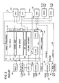
- FIG. 2 a diagram of a prior-art high speed DRAM memory chip is illustrated which implements the waveforms of Fig. 1.
- a pair of 64K arrays of storage cells 10 and 12 are accessed by a column decoder 14 and a wordline (row) driver 16. Row addresses are received into row address buffer 18 and column addresses are received into column address buffer 20.
- a RAS signal, generated by the CPU, is applied via terminal 22 to RASGEN circuit 24 which, in turn, generates two signals. The first is a signal designated PRASBI which tells row address buffer 18 to latch the row (word) address signals. This occurs at time B in Fig. 1. Row address buffer 18 immediately manifests true and complement signals corresponding to the row addresses on line 26.
- RASGEN circuit 24 also generates a signal denoted PRASBII (a signal that initiates a new memory cycle).
- PRASBII a signal that initiates a new memory cycle.
- the PRASBII signal causes a boost wordline clock (BWL) 28 to be triggered.
- BWL boost wordline clock
- an output from BWL 28 is applied to wordline drivers 16 and sample array 34.
- the address true and complement signals on line 26 are decoded in row address decoder (RPD) 30 and applied to word line drivers 16.
- RPD row address decoder
- the output from BWL 28 causes the word lines to be gated to access arrays 12 and 16 in accordance with the decoded address signals and also causes the latching of read-out data in sense amplifiers 32.
- sense amplifiers 32 The latching of sense amplifiers 32 is caused by an output from sample array 34 which, in turn, causes trigger latch clock (PSCG) 36 to transmit an output to sense amp latching clock 38 (PSBCG).
- PSCG trigger latch clock
- PSBCG sense amp latching clock 38
- a reset/precharge circuit 33 is responsive to an output from row address decoder 30, via line 31 to reset/precharge circuit 33 and enables that circuit to reset and precharge the memory circuits within arrays 10 and 12.
- the level on line 31 only provides an activating input to reset/precharge circuits 33 when the address inputs to decoder 30 are inactive. When the address circuits become active, reset precharge circuit 33 is deactivated. Since the circuit of Fig. 2 is in the prior art, its additional detailed operation will not be further described.
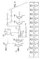
- FIG. 4 a DRAM is shown that incorporates the invention.
- RASGEN circuit 24 has been modified to provide a new signal PRASD, and the timing and functions of PRASBI and PRASBII have been changed.
- Row address buffer 18 now latches in row addresses when PRASBI becomes active.
- the outputs from row address buffer 18 (ADRS T/C) are delayed until activation of the PRASD signal on line 42 from RASGEN circuit 24.
- the RAS signal is applied via terminal 22, to transistors Q2 and Q1 and then through transistors Q6 and Q5 to node 3 and an input to NOR circuit 50. So long as a NOR condition is present at the inputs to NOR circuit 50, its output is at an active level. This causes the PRASBI, PRASBII, and PRASD signals to be at the high or inactive state.
- fuse 52 is blown, and causes a signal appearing at node 3 to be applied through delay circuit 54 to an input to NOR circuit 50.
- delay circuit 54 The details of delay circuit 54 are shown expanded at 56 in Fig. 5). Consequently, an active output at node 5 from NOR circuit 50 is present only after the level at node 3 transitions from the high state to the low state (indicating the termination of the RAS reset/precharge state) and that transition is delayed and arrives at NOR circuit 50 via delay 54.
- the PRASD and PRASBII signals derived when node 5 transitions to the active state are activated at the end of the delayed RAS signal.
- the PRASBI signal appearing at node 58 is activated when node 3 goes low and immediately causes the row addresses in row address buffer 18 to be latched.
- fuse 52 is not blown and the circuit operates as the prior art circuit shown in Fig. 2.
- Fig. 6 a schematic diagram of row address buffer circuit 18 is shown.
- the circuit is modification of a prior circuit shown in U.S. Patent 4,697,108 to Chappell et al.
- the modified portion is shown in dotted box 60.
- the address true and complement signals appear at terminals 62 and 64 respectively. They are gated by the PRASD signal appearing on terminal 64 through NAND GATES 67 and 69. As soon as the PRASBI signal on terminal 66 is activated, the circuit latches the addresses appearing on row address input 68. The address true and complement outputs on terminals 62 and 64 do not become active until the PRASD signal on terminal input 64 is asserted.
- the RAS reset/precharge time is extended by an on-chip generated control signal derived from NOR circuit 50 in Fig. 5. That output and its duration is controlled by the fall at node 3 of the RAS signal and its time delay through delay circuit 54.
- the extension by the delay circuit is only a fraction of the RAS reset time, thus enabling more accurate timing of the RAS cycle.
Landscapes
- Engineering & Computer Science (AREA)
- Microelectronics & Electronic Packaging (AREA)
- Computer Hardware Design (AREA)
- Dram (AREA)
Applications Claiming Priority (2)
| Application Number | Priority Date | Filing Date | Title |
|---|---|---|---|
| US07/545,797 US5185719A (en) | 1989-10-14 | 1990-06-29 | High speed dynamic, random access memory with extended reset/precharge time |
| US545797 | 2000-04-07 |
Publications (3)
| Publication Number | Publication Date |
|---|---|
| EP0468135A2 true EP0468135A2 (de) | 1992-01-29 |
| EP0468135A3 EP0468135A3 (en) | 1994-08-17 |
| EP0468135B1 EP0468135B1 (de) | 1997-05-28 |
Family
ID=24177584
Family Applications (1)
| Application Number | Title | Priority Date | Filing Date |
|---|---|---|---|
| EP19910104396 Expired - Lifetime EP0468135B1 (de) | 1990-06-29 | 1991-03-21 | Dynamischer wahlfreier Speicher mit hoher Geschwindigkeit und verlängerter Rückstell-/Vorladezeit |
Country Status (3)
| Country | Link |
|---|---|
| EP (1) | EP0468135B1 (de) |
| JP (1) | JPH06103595B2 (de) |
| DE (1) | DE69126253D1 (de) |
Cited By (2)
| Publication number | Priority date | Publication date | Assignee | Title |
|---|---|---|---|---|
| GB2287112A (en) * | 1994-03-03 | 1995-09-06 | Samsung Electronics Co Ltd | Auto-precharging semiconductor memory devices |
| USRE36532E (en) * | 1995-03-02 | 2000-01-25 | Samsung Electronics Co., Ltd. | Synchronous semiconductor memory device having an auto-precharge function |
Families Citing this family (1)
| Publication number | Priority date | Publication date | Assignee | Title |
|---|---|---|---|---|
| US7166900B1 (en) * | 2005-08-17 | 2007-01-23 | Infineon Technologies Ag | Semiconductor memory device |
Family Cites Families (4)
| Publication number | Priority date | Publication date | Assignee | Title |
|---|---|---|---|---|
| JPS6052513B2 (ja) * | 1981-12-02 | 1985-11-19 | 富士通株式会社 | 半導体記憶装置 |
| JP2511910B2 (ja) * | 1986-11-11 | 1996-07-03 | 三菱電機株式会社 | 半導体記憶装置 |
| JPS63133395A (ja) * | 1986-11-25 | 1988-06-06 | Toshiba Corp | 半導体記憶装置 |
| JPS63244494A (ja) * | 1987-03-31 | 1988-10-11 | Toshiba Corp | 半導体記憶装置 |
-
1991
- 1991-03-21 EP EP19910104396 patent/EP0468135B1/de not_active Expired - Lifetime
- 1991-03-21 DE DE69126253T patent/DE69126253D1/de not_active Expired - Lifetime
- 1991-05-15 JP JP3138640A patent/JPH06103595B2/ja not_active Expired - Lifetime
Cited By (3)
| Publication number | Priority date | Publication date | Assignee | Title |
|---|---|---|---|---|
| GB2287112A (en) * | 1994-03-03 | 1995-09-06 | Samsung Electronics Co Ltd | Auto-precharging semiconductor memory devices |
| GB2287112B (en) * | 1994-03-03 | 1998-07-29 | Samsung Electronics Co Ltd | Auto-precharging semiconductor memory devices |
| USRE36532E (en) * | 1995-03-02 | 2000-01-25 | Samsung Electronics Co., Ltd. | Synchronous semiconductor memory device having an auto-precharge function |
Also Published As
| Publication number | Publication date |
|---|---|
| JPH06103595B2 (ja) | 1994-12-14 |
| EP0468135B1 (de) | 1997-05-28 |
| JPH04229482A (ja) | 1992-08-18 |
| DE69126253D1 (de) | 1997-07-03 |
| EP0468135A3 (en) | 1994-08-17 |
Similar Documents
| Publication | Publication Date | Title |
|---|---|---|
| JP2851503B2 (ja) | 集積回路記憶装置 | |
| US6128237A (en) | Method and apparatus for enhancing the performance of semiconductor memory devices | |
| US5636174A (en) | Fast cycle time-low latency dynamic random access memories and systems and methods using the same | |
| US7349277B2 (en) | Method and system for reducing the peak current in refreshing dynamic random access memory devices | |
| JP3140461B2 (ja) | ランダム・アクセス・メモリ | |
| US6463002B2 (en) | Refresh-type memory with zero write recovery time and no maximum cycle time | |
| US4943944A (en) | Semiconductor memory using dynamic ram cells | |
| US5185719A (en) | High speed dynamic, random access memory with extended reset/precharge time | |
| KR940008882B1 (ko) | 집적 회로의 랜덤 액세스 메모리 | |
| US5293347A (en) | Semiconductor memory device having read/write operation improved in pipe line processing | |
| US7821831B2 (en) | Block erase for volatile memory | |
| US6130843A (en) | Method and circuit for providing a memory device having hidden row access and row precharge times | |
| CA2313954A1 (en) | High speed dram architecture with uniform latency | |
| JPH0793009B2 (ja) | 半導体記憶装置 | |
| JPH07176186A (ja) | ダイナミックランダムアクセスメモリおよびそのリフレッシュ方法 | |
| US5563835A (en) | Sense amplification in data memories | |
| US4581722A (en) | Dynamic random access memory having small cycle time period | |
| US6108254A (en) | Dynamic random access memory having continuous data line equalization except at address transition during data reading | |
| US6205069B1 (en) | Semiconductor memory device with fast input/output line precharge scheme and method of precharging input/output lines thereof | |
| JPH041955B2 (de) | ||
| EP0037252B1 (de) | Dynamischer Halbleiterspeicher | |
| US6456563B1 (en) | Semiconductor memory device that operates in sychronization with a clock signal | |
| US5007028A (en) | Multiport memory with improved timing of word line selection | |
| US4354259A (en) | Semiconductor memory device having improved column selection structure | |
| EP0468135B1 (de) | Dynamischer wahlfreier Speicher mit hoher Geschwindigkeit und verlängerter Rückstell-/Vorladezeit |
Legal Events
| Date | Code | Title | Description |
|---|---|---|---|
| PUAI | Public reference made under article 153(3) epc to a published international application that has entered the european phase |
Free format text: ORIGINAL CODE: 0009012 |
|
| AK | Designated contracting states |
Kind code of ref document: A2 Designated state(s): DE FR GB |
|
| 17P | Request for examination filed |
Effective date: 19911219 |
|
| PUAL | Search report despatched |
Free format text: ORIGINAL CODE: 0009013 |
|
| AK | Designated contracting states |
Kind code of ref document: A3 Designated state(s): DE FR GB |
|
| 17Q | First examination report despatched |
Effective date: 19960110 |
|
| GRAG | Despatch of communication of intention to grant |
Free format text: ORIGINAL CODE: EPIDOS AGRA |
|
| GRAH | Despatch of communication of intention to grant a patent |
Free format text: ORIGINAL CODE: EPIDOS IGRA |
|
| GRAH | Despatch of communication of intention to grant a patent |
Free format text: ORIGINAL CODE: EPIDOS IGRA |
|
| GRAA | (expected) grant |
Free format text: ORIGINAL CODE: 0009210 |
|
| AK | Designated contracting states |
Kind code of ref document: B1 Designated state(s): DE FR GB |
|
| PG25 | Lapsed in a contracting state [announced via postgrant information from national office to epo] |
Ref country code: FR Free format text: THE PATENT HAS BEEN ANNULLED BY A DECISION OF A NATIONAL AUTHORITY Effective date: 19970528 |
|
| REF | Corresponds to: |
Ref document number: 69126253 Country of ref document: DE Date of ref document: 19970703 |
|
| ET | Fr: translation filed | ||
| PG25 | Lapsed in a contracting state [announced via postgrant information from national office to epo] |
Ref country code: DE Effective date: 19970829 |
|
| PG25 | Lapsed in a contracting state [announced via postgrant information from national office to epo] |
Ref country code: GB Free format text: LAPSE BECAUSE OF NON-PAYMENT OF DUE FEES Effective date: 19980321 |
|
| PLBE | No opposition filed within time limit |
Free format text: ORIGINAL CODE: 0009261 |
|
| STAA | Information on the status of an ep patent application or granted ep patent |
Free format text: STATUS: NO OPPOSITION FILED WITHIN TIME LIMIT |
|
| 26N | No opposition filed | ||
| GBPC | Gb: european patent ceased through non-payment of renewal fee |
Effective date: 19980321 |
|
| REG | Reference to a national code |
Ref country code: FR Ref legal event code: ST |