EP0468463B1 - Halbleiterspeicheranordnung - Google Patents
Halbleiterspeicheranordnung Download PDFInfo
- Publication number
- EP0468463B1 EP0468463B1 EP91112353A EP91112353A EP0468463B1 EP 0468463 B1 EP0468463 B1 EP 0468463B1 EP 91112353 A EP91112353 A EP 91112353A EP 91112353 A EP91112353 A EP 91112353A EP 0468463 B1 EP0468463 B1 EP 0468463B1
- Authority
- EP
- European Patent Office
- Prior art keywords
- potential
- power supply
- mosfet
- reference potential
- supply node
- Prior art date
- Legal status (The legal status is an assumption and is not a legal conclusion. Google has not performed a legal analysis and makes no representation as to the accuracy of the status listed.)
- Expired - Lifetime
Links
- 239000004065 semiconductor Substances 0.000 title claims description 13
- 239000003990 capacitor Substances 0.000 claims description 9
- 230000010355 oscillation Effects 0.000 claims description 7
- 230000008878 coupling Effects 0.000 claims description 4
- 238000010168 coupling process Methods 0.000 claims description 4
- 238000005859 coupling reaction Methods 0.000 claims description 4
- 238000010586 diagram Methods 0.000 description 8
- 238000001514 detection method Methods 0.000 description 2
- 230000006870 function Effects 0.000 description 2
- 230000002452 interceptive effect Effects 0.000 description 2
- 230000003213 activating effect Effects 0.000 description 1
- 230000000903 blocking effect Effects 0.000 description 1
- 230000000295 complement effect Effects 0.000 description 1
- 238000010276 construction Methods 0.000 description 1
- 238000007599 discharging Methods 0.000 description 1
- 230000000694 effects Effects 0.000 description 1
- 238000000034 method Methods 0.000 description 1
- 238000012986 modification Methods 0.000 description 1
- 230000004048 modification Effects 0.000 description 1
- 238000005086 pumping Methods 0.000 description 1
Images


Classifications
-
- G—PHYSICS
- G11—INFORMATION STORAGE
- G11C—STATIC STORES
- G11C11/00—Digital stores characterised by the use of particular electric or magnetic storage elements; Storage elements therefor
- G11C11/21—Digital stores characterised by the use of particular electric or magnetic storage elements; Storage elements therefor using electric elements
- G11C11/34—Digital stores characterised by the use of particular electric or magnetic storage elements; Storage elements therefor using electric elements using semiconductor devices
- G11C11/40—Digital stores characterised by the use of particular electric or magnetic storage elements; Storage elements therefor using electric elements using semiconductor devices using transistors
- G11C11/401—Digital stores characterised by the use of particular electric or magnetic storage elements; Storage elements therefor using electric elements using semiconductor devices using transistors forming cells needing refreshing or charge regeneration, i.e. dynamic cells
- G11C11/4063—Auxiliary circuits, e.g. for addressing, decoding, driving, writing, sensing or timing
- G11C11/407—Auxiliary circuits, e.g. for addressing, decoding, driving, writing, sensing or timing for memory cells of the field-effect type
-
- G—PHYSICS
- G11—INFORMATION STORAGE
- G11C—STATIC STORES
- G11C7/00—Arrangements for writing information into, or reading information out from, a digital store
- G11C7/20—Memory cell initialisation circuits, e.g. when powering up or down, memory clear, latent image memory
-
- G—PHYSICS
- G11—INFORMATION STORAGE
- G11C—STATIC STORES
- G11C11/00—Digital stores characterised by the use of particular electric or magnetic storage elements; Storage elements therefor
- G11C11/21—Digital stores characterised by the use of particular electric or magnetic storage elements; Storage elements therefor using electric elements
- G11C11/34—Digital stores characterised by the use of particular electric or magnetic storage elements; Storage elements therefor using electric elements using semiconductor devices
- G11C11/40—Digital stores characterised by the use of particular electric or magnetic storage elements; Storage elements therefor using electric elements using semiconductor devices using transistors
- G11C11/401—Digital stores characterised by the use of particular electric or magnetic storage elements; Storage elements therefor using electric elements using semiconductor devices using transistors forming cells needing refreshing or charge regeneration, i.e. dynamic cells
- G11C11/4063—Auxiliary circuits, e.g. for addressing, decoding, driving, writing, sensing or timing
- G11C11/407—Auxiliary circuits, e.g. for addressing, decoding, driving, writing, sensing or timing for memory cells of the field-effect type
- G11C11/4072—Circuits for initialization, powering up or down, clearing memory or presetting
Definitions
- the invention in its second embodiment, employs, in place of the negative potential input section in the first embodiment of the invention, a negative potential supplying section capable of being selectively made active or inactive and producing, when active, a negative potential, and supplying it to the power supply node, and a control section which is responsive to a control signal, for turning off the switching section and activating the negative potential supplying section.
- the reference potential supplying section and the negative potential input section are provided, and by inputting the external signal of a negative potential, the reference potential from the reference potential supplying section is blocked, and the input external signal is supplied via the negative potential input section to the power supply node. Accordingly, by inputting the external signal of a negative potential, the memory cells are simply and quickly initialized to the physical "0" state, and an efficient simultaneous erasure can be achieved.
Landscapes
- Engineering & Computer Science (AREA)
- Microelectronics & Electronic Packaging (AREA)
- Computer Hardware Design (AREA)
- Dram (AREA)
- Static Random-Access Memory (AREA)
- Semiconductor Memories (AREA)
Claims (14)
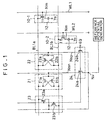
- Halbleiterspeichervorrichtung, die folgendes aufweist:eine Vielzahl von Speicherzellen (10-1, 10-2), die jeweils an den Schnittpunkten einer Vielzahl von Bitleitungen (BL1a, BL1b) und einer Vielzahl von Wortleitungen (WL1, WL2) angeschlossen sind;eine Vielzahl von Abfühlverstärkern (21, 22), die durch ein Potential auf einem gemeinsamen Knoten (Nsn, Nsp) aktiviert werden, um die Potentialdifferenzen eines jeweiligen Paares der Bitleitungen abzufühlen und zu verstärken, dadurch gekennzeichnet, daß die Halbleiterspeichervorrichtung weiterhin folgendes aufweist:eine Ausgleichseinrichtung (23), die durch ein Ausgleichssignal (EQ) aktiviert wird, um das Potential auf einem oberen Stromversorgungsknoten (Nv) an die jeweiligen Paar der Bitleitungen anzulegen;eine Einrichtung zum Zuführen eines Bezugspotentials (30), zur Erzeugung eines Bezugspotentials und um das Bezugspotential über eine Schalteinrichtung (32) dem Stromversorgungsknoten (Nv) zuzuführen; undeine Einrichtung zum Anlegen eines negativen Potentials (40, 50, 60), zum Anlegen eines negativen Potentials an den Stromversorgungsknoten (Nv), um eine Initialisierung durchzuführen.
- Vorrichtung nach Anspruch 1, wobei die Einrichtung zum Anlegen eines negativen Potentials folgendes aufweist:
eine Eingabeeinrichtung für ein negatives Potential (40), zum Empfang eines externen Signals (S41) mit einem negativen Potential und zum Ausschalten der Schalteinrichtung (32) und um dem Stromversorgungsknoten (Nv) das externe Signal zuzuführen. - Vorrichtung nach Anspruch 1 oder 2, wobeidie Einrichtung zum Zuführen eines Bezugspotentials weiterhin einen Bezugspotentialgenerator (31) zum Zuführen des Bezugspotentials aufweist;die Schalteinrichtung das Anlegen des Bezugspotentials an den Stromversorgungsknoten (Nv) zuläßt, wenn sie Ein ist, und das Anlegen des Bezugspotentials an den Stromversorgungsknoten sperrt, wenn sie Aus ist.
- Vorrichtung nach Anspruch 1 oder 2, wobei die Schalteinrichtung folgendes aufweist:einen ersten MOSFET (32c), der den Bezugspotentialgenerator (31) und den Stromversorgungsknoten (Nv) verbindet;einen zweiten MOSFET (32a), der Aus ist, wenn das externe Signal aktiv ist, und der Ein ist, wenn das externe Signal inaktiv ist; undeinen dritten MOSFET (32b), der Aus ist, wenn das externe Signal inaktiv ist, und der Ein ist, wenn das externe Signal aktiv ist;wobei der erste MOSFET Ein ist, wenn der zweite MOSFET Ein ist und der dritte MOSFET Aus ist, und Aus ist, wenn der zweite MOSFET Aus ist und der dritte MOSFET Ein ist.
- Vorrichtung nach Anspruch 2, wobei die Eingabeeinrichtung für ein negatives Potential einen Invertierer (42), der das externe Signal empfängt und ein Umkehrsignal des Eingangssignals erzeugt, und eine Einrichtung zum Anlegen des Umkehrsignals an die Schalteinrichtung der Einrichtung zum Zuführen eines Bezugspotentials aufweist.
- Vorrichtung nach Anspruch 4, wobei die Eingabeeinrichtung für ein negatives Potential eine Schalteinrichtung (43) aufweist, die durch das Umkehrsignal eingeschaltet wird, um das Anlegen des externen Signals an den Stromversorgungsknoten (Nv) zuzulassen.
- Halbleiterspeichervorrichtung gemäß Anspruch 1, wobei die Einrichtung zum Anlegen eines negativen Potentials (40, 50, 60) folgendes aufweist:eine Einrichtung zum Zuführen eines negativen Potentials (60), die imstande ist, selektiv aktiviert oder inaktiviert zu werden und, wenn sie aktiv ist, dem Stromversorgungsknoten ein negatives Potential zuzuführen; undeine Steuereinrichtung (50), die ein Steuersignal (CS) empfängt und die, wenn das Steuersignal in einem ersten Zustand ist, die Schalteinrichtung (32) ausschaltet und die Einrichtung zum Zuführen eines negativen Potentials (60) aktiviert und die, wenn das Steuersignal in einem zweiten Zustand ist, die Schalteinrichtung (32) einschaltet und die Einrichtung zum Zuführen eines negativen Potentials (60) inaktiviert.
- Vorrichtung nach Anspruch 7, wobei die Einrichtung zum Zuführen eines negativen Potentials folgendes aufweist:einen Ringoszillator (61);einen Schalttransistor (66), der Ein ist, wenn das Steuersignal in dem zweiten Zustand ist, um das Schwingen des Ringoszillators zu verhindern, und der Aus ist, wenn das Steuersignal in dem ersten Zustand ist, um das Schwingen des Ringoszillators zuzulassen.
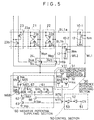
- Vorrichtung nach Anspruch 8, wobei die Einrichtung zum Zuführen eines negativen Potentials (60) weiterhin folgendes aufweist:einen Kopplungskondensator (67) mit einer ersten Elektrode, die mit einem Ausgangsknoten (N61) des Ringoszillators (61) verbunden ist, und einer zweiten Elektrode;eine erste Gleichrichterschaltung (62) mit einer Anode, die mit der zweiten Elektrode des Kondensators (67) verbunden ist;einen Schalttransistor (63) mit einem Drain, der mit der Kathode der ersten Gleichrichterschaltung (62) verbunden ist, und einer geerdeten Source;eine zweite Gleichrichterschaltung (64, 65) mit einer geerdeten Anode und einer Kathode;eine dritte Gleichrichterschaltung (68) mit einer Anode, die mit der Kathode der zweiten Gleichrichterschaltung verbunden ist, und einer Kathode, die mit der zweiten Elektrode des Kondensators verbunden ist;wobei die Kathode der zweiten Gleichrichterschaltung den Ausgangsknoten der Einrichtung zur Erzeugung eines negativen Potentials bildet, der mit dem Stromversorgungsknoten (Nv) verbunden ist.
- Vorrichtung nach Anspruch 9, wobeidie Einrichtung zum Zuführen eines Bezugspotentials weiterhin einen Bezugspotentialgenerator (31) zum Zuführen des Bezugspotentials aufweist;die Schalteinrichtung das Anlegen des Bezugspotentials an den Stromversorgungsknoten (Nv) zuläßt, wenn sie Ein ist, und das Anlegen des Bezugspotentials an den Stromversorgungsknoten sperrt, wenn sie Aus ist.
- Vorrichtung nach Anspruch 10, wobei die Schalteinrichtung folgendes aufweist:einen ersten MOSFET (32c), der den Bezugspotentialgenerator (31) und den Stromversorgungsknoten (Nv) verbindet;einen zweiten MOSFET (32a), der Aus ist, wenn das externe Signal aktiv ist, und der Ein ist, wenn das externe Signal inaktiv ist; undeinen dritten MOSFET (32b), der Aus ist, wenn das externe Signal inaktiv ist, und der Ein ist, wenn das externe Signal aktiv ist;wobei der erste MOSFET Ein ist, wenn der zweite MOSFET Ein ist und der dritte MOSFET Aus ist, und Aus ist, wenn der zweite MOSFET Aus ist und der dritte MOSFET Ein ist.
- Vorrichtung nach Anspruch 11, wobei die zweite Gleichrichterschaltung (64, 65) einen ersten Gleichrichter (65) mit einer geerdeten Anode und einer Kathode und einen zweiten Gleichrichter (64) mit einer Anode, die mit der Kathode des ersten Gleichrichters (65) verbunden ist, und mit einer Kathode, die mit dem Stromversorgungsknoten (Nv) verbunden ist, aufweist; und wobei das Potential auf der Kathode des ersten Gleichrichters (65) der zweiten Gleichrichterschaltung (64, 65) verwendet wird, um den ersten MOSFET (32c) der Schalteinrichtung auszuschalten.
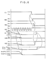
- Vorrichtung nach Anspruch 7, wobeidie Steuereinrichtung (50) einen ersten Invertierer (52), der das Steuersignal (CS) empfängt, und einen zweiten Invertierer (53) aufweist, der das Ausgangssignal des ersten Invertierers (52) empfängt;der Ringoszillator zum Schwingen gebracht wird, wenn der Ausgang des zweiten Invertierers tiefpegelig ist;die Schalteinrichtung (32) der Einrichtung zum Zuführen eines Bezugspotentials (30) Aus ist, wenn der Ausgang des zweiten Invertierers (53) hochpegelig ist; undder MOSFET (63) Ein ist, wenn der Ausgang des zweiten Invertierers (53) hochpegelig ist.
- Vorrichtung nach Anspruch 7, die weiterhin folgendes aufweist:
eine Detektoreinrichtung für ein hohes Potential (70), die auf ein Signal reagiert, das ein Potential aufweist, das einen Bereich von unter normalen Lese/Schreib-Betriebsbedingungen angelegten Potentialen übersteigt, um das Steuersignal in den ersten Zustand zu bringen und um das Steuersignal zu anderen Zeiten in den zweiten Zustand zu bringen.
Applications Claiming Priority (2)
| Application Number | Priority Date | Filing Date | Title |
|---|---|---|---|
| JP194666/90 | 1990-07-23 | ||
| JP2194666A JP2963504B2 (ja) | 1990-07-23 | 1990-07-23 | 半導体記憶装置 |
Publications (3)
| Publication Number | Publication Date |
|---|---|
| EP0468463A2 EP0468463A2 (de) | 1992-01-29 |
| EP0468463A3 EP0468463A3 (en) | 1993-05-12 |
| EP0468463B1 true EP0468463B1 (de) | 1997-01-08 |
Family
ID=16328291
Family Applications (1)
| Application Number | Title | Priority Date | Filing Date |
|---|---|---|---|
| EP91112353A Expired - Lifetime EP0468463B1 (de) | 1990-07-23 | 1991-07-23 | Halbleiterspeicheranordnung |
Country Status (5)
| Country | Link |
|---|---|
| US (1) | US5255223A (de) |
| EP (1) | EP0468463B1 (de) |
| JP (1) | JP2963504B2 (de) |
| KR (1) | KR960011555B1 (de) |
| DE (1) | DE69124022T2 (de) |
Families Citing this family (6)
| Publication number | Priority date | Publication date | Assignee | Title |
|---|---|---|---|---|
| US5235550A (en) * | 1991-05-16 | 1993-08-10 | Micron Technology, Inc. | Method for maintaining optimum biasing voltage and standby current levels in a DRAM array having repaired row-to-column shorts |
| JP3358030B2 (ja) * | 1993-01-22 | 2002-12-16 | 日本テキサス・インスツルメンツ株式会社 | 半導体メモリ装置及びその初期化方法 |
| IT1286072B1 (it) * | 1996-10-31 | 1998-07-07 | Sgs Thomson Microelectronics | Equalizzatore autoregolato,in particolare per amplificatore di rilevamento,o sense amplifier |
| JP2000036194A (ja) * | 1998-07-16 | 2000-02-02 | Nec Corp | 半導体記憶装置 |
| US20090312626A1 (en) * | 2008-06-12 | 2009-12-17 | Hanrahan Christopher J | Articles and methods for improving mri imaging |
| KR101155451B1 (ko) | 2011-08-31 | 2012-06-15 | 테세라, 인코포레이티드 | Dram 보안 소거 |
Family Cites Families (5)
| Publication number | Priority date | Publication date | Assignee | Title |
|---|---|---|---|---|
| JPS60253093A (ja) * | 1984-05-30 | 1985-12-13 | Fujitsu Ltd | 半導体記憶装置 |
| US4780850A (en) * | 1986-10-31 | 1988-10-25 | Mitsubishi Denki Kabushiki Kaisha | CMOS dynamic random access memory |
| JPS6457490A (en) * | 1987-08-28 | 1989-03-03 | Mitsubishi Electric Corp | Dynamic ram |
| JPH0283892A (ja) * | 1988-09-20 | 1990-03-23 | Fujitsu Ltd | 半導体記憶装置 |
| JPH07118196B2 (ja) * | 1988-12-28 | 1995-12-18 | 株式会社東芝 | スタティック型半導体メモリ |
-
1990
- 1990-07-23 JP JP2194666A patent/JP2963504B2/ja not_active Expired - Fee Related
-
1991
- 1991-06-21 KR KR1019910010346A patent/KR960011555B1/ko not_active Expired - Fee Related
- 1991-07-17 US US07/731,337 patent/US5255223A/en not_active Expired - Lifetime
- 1991-07-23 EP EP91112353A patent/EP0468463B1/de not_active Expired - Lifetime
- 1991-07-23 DE DE69124022T patent/DE69124022T2/de not_active Expired - Fee Related
Also Published As
| Publication number | Publication date |
|---|---|
| KR920003309A (ko) | 1992-02-29 |
| US5255223A (en) | 1993-10-19 |
| DE69124022D1 (de) | 1997-02-20 |
| EP0468463A3 (en) | 1993-05-12 |
| JP2963504B2 (ja) | 1999-10-18 |
| EP0468463A2 (de) | 1992-01-29 |
| DE69124022T2 (de) | 1997-08-14 |
| KR960011555B1 (ko) | 1996-08-23 |
| JPH0482081A (ja) | 1992-03-16 |
Similar Documents
| Publication | Publication Date | Title |
|---|---|---|
| US3959781A (en) | Semiconductor random access memory | |
| US4694427A (en) | Programmable semiconductor memory device with combined sense amplification and programming capability | |
| US4087704A (en) | Sequential timing circuitry for a semiconductor memory | |
| US5119334A (en) | Dynamic random access memory having improved word line control | |
| KR0183413B1 (ko) | 차지-펌프형 부스터 회로 | |
| JP3037377B2 (ja) | 半導体記憶装置 | |
| US5555526A (en) | Synchronous semiconductor memory device having an auto-precharge function | |
| US7560976B2 (en) | Method of operating a semiconductor device and the semiconductor device | |
| US6504783B2 (en) | Semiconductor device having early operation high voltage generator and high voltage supplying method therefor | |
| JP2006318642A (ja) | ダイナミックランダムアクセスメモリ | |
| KR100297717B1 (ko) | 반도체메모리의입출력선프리차아지회로및이를사용하는반도체메모리 | |
| JPH087997B2 (ja) | ランダムアクセスメモリ装置 | |
| JP2626636B2 (ja) | ダイナミックランダムアクセスメモリ装置 | |
| KR950009074B1 (ko) | 다이너믹형 반도체 기억장치 | |
| JP3735824B2 (ja) | 昇圧回路を備えた半導体メモリ装置 | |
| EP0468463B1 (de) | Halbleiterspeicheranordnung | |
| JP3786977B2 (ja) | 低電源電圧を使用する半導体メモリ装置 | |
| US5414671A (en) | Semiconductor memory device having operation control means with data judging function | |
| US7307901B2 (en) | Apparatus and method for improving dynamic refresh in a memory device | |
| KR100294450B1 (ko) | 반도체메모리장치의어레이내부전원전압발생회로 | |
| USRE36532E (en) | Synchronous semiconductor memory device having an auto-precharge function | |
| US5777934A (en) | Semiconductor memory device with variable plate voltage generator | |
| US5408437A (en) | Static random access memory | |
| JPH0115958B2 (de) | ||
| US6256244B1 (en) | Self refresh apparatus in semiconductor memory device |
Legal Events
| Date | Code | Title | Description |
|---|---|---|---|
| PUAI | Public reference made under article 153(3) epc to a published international application that has entered the european phase |
Free format text: ORIGINAL CODE: 0009012 |
|
| AK | Designated contracting states |
Kind code of ref document: A2 Designated state(s): DE FR NL |
|
| PUAL | Search report despatched |
Free format text: ORIGINAL CODE: 0009013 |
|
| AK | Designated contracting states |
Kind code of ref document: A3 Designated state(s): DE FR NL |
|
| 17P | Request for examination filed |
Effective date: 19930727 |
|
| 17Q | First examination report despatched |
Effective date: 19950814 |
|
| GRAG | Despatch of communication of intention to grant |
Free format text: ORIGINAL CODE: EPIDOS AGRA |
|
| GRAH | Despatch of communication of intention to grant a patent |
Free format text: ORIGINAL CODE: EPIDOS IGRA |
|
| GRAH | Despatch of communication of intention to grant a patent |
Free format text: ORIGINAL CODE: EPIDOS IGRA |
|
| GRAA | (expected) grant |
Free format text: ORIGINAL CODE: 0009210 |
|
| AK | Designated contracting states |
Kind code of ref document: B1 Designated state(s): DE FR NL |
|
| REF | Corresponds to: |
Ref document number: 69124022 Country of ref document: DE Date of ref document: 19970220 |
|
| ET | Fr: translation filed | ||
| PLBE | No opposition filed within time limit |
Free format text: ORIGINAL CODE: 0009261 |
|
| STAA | Information on the status of an ep patent application or granted ep patent |
Free format text: STATUS: NO OPPOSITION FILED WITHIN TIME LIMIT |
|
| 26N | No opposition filed | ||
| PGFP | Annual fee paid to national office [announced via postgrant information from national office to epo] |
Ref country code: FR Payment date: 20010712 Year of fee payment: 11 |
|
| PGFP | Annual fee paid to national office [announced via postgrant information from national office to epo] |
Ref country code: DE Payment date: 20010716 Year of fee payment: 11 |
|
| PGFP | Annual fee paid to national office [announced via postgrant information from national office to epo] |
Ref country code: NL Payment date: 20010730 Year of fee payment: 11 |
|
| PG25 | Lapsed in a contracting state [announced via postgrant information from national office to epo] |
Ref country code: NL Free format text: LAPSE BECAUSE OF NON-PAYMENT OF DUE FEES Effective date: 20030201 Ref country code: DE Free format text: LAPSE BECAUSE OF NON-PAYMENT OF DUE FEES Effective date: 20030201 |
|
| PG25 | Lapsed in a contracting state [announced via postgrant information from national office to epo] |
Ref country code: FR Free format text: LAPSE BECAUSE OF NON-PAYMENT OF DUE FEES Effective date: 20030331 |
|
| NLV4 | Nl: lapsed or anulled due to non-payment of the annual fee |
Effective date: 20030201 |
|
| REG | Reference to a national code |
Ref country code: FR Ref legal event code: ST |