EP0468897A1 - Verfahren zur Bestimmung der vollständigen Abtragung einer Dünnschicht auf einem nichtplanaren Substrat - Google Patents
Verfahren zur Bestimmung der vollständigen Abtragung einer Dünnschicht auf einem nichtplanaren Substrat Download PDFInfo
- Publication number
- EP0468897A1 EP0468897A1 EP91420256A EP91420256A EP0468897A1 EP 0468897 A1 EP0468897 A1 EP 0468897A1 EP 91420256 A EP91420256 A EP 91420256A EP 91420256 A EP91420256 A EP 91420256A EP 0468897 A1 EP0468897 A1 EP 0468897A1
- Authority
- EP
- European Patent Office
- Prior art keywords
- thin layer
- substrate
- diffraction grating
- diffraction
- layer
- Prior art date
- Legal status (The legal status is an assumption and is not a legal conclusion. Google has not performed a legal analysis and makes no representation as to the accuracy of the status listed.)
- Granted
Links
Images
Classifications
-
- B—PERFORMING OPERATIONS; TRANSPORTING
- B24—GRINDING; POLISHING
- B24B—MACHINES, DEVICES, OR PROCESSES FOR GRINDING OR POLISHING; DRESSING OR CONDITIONING OF ABRADING SURFACES; FEEDING OF GRINDING, POLISHING, OR LAPPING AGENTS
- B24B37/00—Lapping machines or devices; Accessories
- B24B37/005—Control means for lapping machines or devices
- B24B37/013—Devices or means for detecting lapping completion
-
- H—ELECTRICITY
- H01—ELECTRIC ELEMENTS
- H01J—ELECTRIC DISCHARGE TUBES OR DISCHARGE LAMPS
- H01J37/00—Discharge tubes with provision for introducing objects or material to be exposed to the discharge, e.g. for the purpose of examination or processing thereof
- H01J37/32—Gas-filled discharge tubes
- H01J37/32917—Plasma diagnostics
- H01J37/32935—Monitoring and controlling tubes by information coming from the object and/or discharge
-
- H—ELECTRICITY
- H01—ELECTRIC ELEMENTS
- H01J—ELECTRIC DISCHARGE TUBES OR DISCHARGE LAMPS
- H01J37/00—Discharge tubes with provision for introducing objects or material to be exposed to the discharge, e.g. for the purpose of examination or processing thereof
- H01J37/32—Gas-filled discharge tubes
- H01J37/32917—Plasma diagnostics
- H01J37/32935—Monitoring and controlling tubes by information coming from the object and/or discharge
- H01J37/32963—End-point detection
-
- H—ELECTRICITY
- H10—SEMICONDUCTOR DEVICES; ELECTRIC SOLID-STATE DEVICES NOT OTHERWISE PROVIDED FOR
- H10P—GENERIC PROCESSES OR APPARATUS FOR THE MANUFACTURE OR TREATMENT OF DEVICES COVERED BY CLASS H10
- H10P50/00—Etching of wafers, substrates or parts of devices
- H10P50/20—Dry etching; Plasma etching; Reactive-ion etching
- H10P50/26—Dry etching; Plasma etching; Reactive-ion etching of conductive or resistive materials
- H10P50/264—Dry etching; Plasma etching; Reactive-ion etching of conductive or resistive materials by chemical means
- H10P50/266—Dry etching; Plasma etching; Reactive-ion etching of conductive or resistive materials by chemical means by vapour etching only
- H10P50/267—Dry etching; Plasma etching; Reactive-ion etching of conductive or resistive materials by chemical means by vapour etching only using plasmas
- H10P50/268—Dry etching; Plasma etching; Reactive-ion etching of conductive or resistive materials by chemical means by vapour etching only using plasmas of silicon-containing layers
-
- H—ELECTRICITY
- H10—SEMICONDUCTOR DEVICES; ELECTRIC SOLID-STATE DEVICES NOT OTHERWISE PROVIDED FOR
- H10P—GENERIC PROCESSES OR APPARATUS FOR THE MANUFACTURE OR TREATMENT OF DEVICES COVERED BY CLASS H10
- H10P74/00—Testing or measuring during manufacture or treatment of wafers, substrates or devices
- H10P74/23—Testing or measuring during manufacture or treatment of wafers, substrates or devices characterised by multiple measurements, corrections, marking or sorting processes
- H10P74/238—Testing or measuring during manufacture or treatment of wafers, substrates or devices characterised by multiple measurements, corrections, marking or sorting processes comprising acting in response to an ongoing measurement without interruption of processing, e.g. endpoint detection or in-situ thickness measurement
-
- H—ELECTRICITY
- H10—SEMICONDUCTOR DEVICES; ELECTRIC SOLID-STATE DEVICES NOT OTHERWISE PROVIDED FOR
- H10W—GENERIC PACKAGES, INTERCONNECTIONS, CONNECTORS OR OTHER CONSTRUCTIONAL DETAILS OF DEVICES COVERED BY CLASS H10
- H10W20/00—Interconnections in chips, wafers or substrates
- H10W20/01—Manufacture or treatment
- H10W20/031—Manufacture or treatment of conductive parts of the interconnections
- H10W20/056—Manufacture or treatment of conductive parts of the interconnections by filling conductive material into holes, grooves or trenches
-
- H—ELECTRICITY
- H01—ELECTRIC ELEMENTS
- H01J—ELECTRIC DISCHARGE TUBES OR DISCHARGE LAMPS
- H01J2237/00—Discharge tubes exposing object to beam, e.g. for analysis treatment, etching, imaging
- H01J2237/30—Electron or ion beam tubes for processing objects
- H01J2237/304—Controlling tubes
- H01J2237/30466—Detecting endpoint of process
-
- H—ELECTRICITY
- H01—ELECTRIC ELEMENTS
- H01J—ELECTRIC DISCHARGE TUBES OR DISCHARGE LAMPS
- H01J2237/00—Discharge tubes exposing object to beam, e.g. for analysis treatment, etching, imaging
- H01J2237/32—Processing objects by plasma generation
- H01J2237/33—Processing objects by plasma generation characterised by the type of processing
- H01J2237/334—Etching
Definitions
- the present invention relates to a method for detecting the end of attack, and more particularly the complete removal, of a layer deposited on a substrate.
- the invention finds applications in the field of manufacturing integrated circuits, in particular for detecting the end of the attack of a thin metallic layer deposited on a substrate having a certain relief.
- An object of the present invention is to provide a method for the precise determination of the complete elimination of a thin layer deposited on a substrate.
- Another object of the present invention is to provide such a method which can be used as a means of control to verify that an etching operation has been carried out in a satisfactory manner.
- Another object of the present invention is to provide such a method which can be implemented in situ during an etching operation.
- the invention provides a method for determining the complete elimination of a thin layer deposited on a substrate, comprising the steps consisting in providing on an area of substrate an optical diffraction grating, the thin layer deposited on the substrate also covering this diffraction grating, and the attack of the thin layer also taking place at the level of this diffraction grating; illuminate the network with a monochromatic light beam; and observing the evolution of the diffracted light during the etching operation of the thin layer, in order to determine the instant when the material of the thin layer is completely removed.
- the substrate corresponds to a layer of silicon oxide
- the diffraction grating is obtained by anisotropic etching of a determined area of this layer
- the thin layer is metallic
- the diffraction pattern obtained from the grating is compared to diffraction patterns obtained during a calibration.
- a first metal layer is deposited which is etched according to a chosen connection pattern, then an insulating layer, often made of silicon oxide, in which passage holes are provided.
- the insulating layer is deposited by a second metallic layer which fills the through holes.
- a second plate metal etching is then carried out in order to completely remove the metal from this layer present on the underlying insulating layer, and retaining metal only inside the through holes provided in the insulating layer.
- a third metal layer is deposited which is etched according to a chosen connection pattern.
- the etching operation of the second metal layer is particularly delicate. In fact, this etching must be prolonged long enough so that there is no longer any metallic residue on the insulating layer, but this etching operation must not be prolonged beyond to avoid removing too much metal present in through holes.
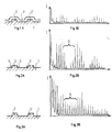
- an insulating layer 1 constituting part of the insulating layer is deposited in an unused area mentioned above.
- an optical diffraction grating consisting of a number of equidistant ribs 2, 2 ′ is formed.
- the height of the ribs is of the same order of magnitude as the height of the steps present on the rest of the plate at the level of the circuits in progress.
- the second metal layer 3 covering the insulating layer 1 also covers the area comprising the diffraction grating 2, 2 ′ and matches the relief of the ribs. The etching of this metal layer 3 takes place in the area comprising the diffraction grating at the same time as in the useful area.
- FIG. 2A shows the same structure when the etching operation of the metal layer 3 is almost completed.
- Residues 5 of the metal of layer 3 exist, these residues being located mainly at the foot of the vertical sides of the diffraction grating or in their vicinity. These residues 5 can have various shapes and have extremely small dimensions. As long as such residues 5 remain, it is advisable to continue the etching operation, until their complete removal, as explained above.
- FIG. 3A represents the structure when the residues have completely disappeared.
- the diffraction grating is illuminated by a monochromatic light beam and the evolution of the diffracted light is observed.
- Figures 1B, 2B and 3B show diffraction figures corresponding to the structures respectively shown in Figures 1A, 2A and 3A. There is a series of intense light spots on either side of the specular reflection spot (only one side of the diffraction pattern is shown in Figures 1B to 3B and only from order 6).
- the diffraction pattern changes continuously at the start of the etching of the metal layer 3.
- This diffraction pattern then changes very significantly when moving from a continuous layer 3 to residues scattered and then when one passes from the etching level corresponding to FIG. 2A to that corresponding to FIG. 3A, that is to say when one passes from a structure in which remain metal residues of very small dimensions, with a structure free of metallic residues.
- the invention therefore makes it possible to very sensitively detect the presence or absence of metal residues of very small dimensions, and this in an almost instantaneous manner, during the course of the etching operation.
- the light intensity measurement of one or more spots can be carried out using an analyzer moving along the diffraction pattern. It is also possible to carry out the measurement by sampling by means of a diode array.
- the liminous beam is for example obtained using a helium / neon type laser operating at a wavelength of 632.8 nm.
- the present invention can also be used for the control of engraved plates.
- the diffraction pattern obtained by lighting up a pattern of ribs 2 having been etched will be compared with diffraction patterns obtained previously during the calibration phases.
- This control process has the advantage of being precise, non-destructive and non-polluting.
- a diffraction grating has been previously described specially formed in an unused area of the substrate, one could use a pattern formed in a part of the circuit during manufacture, for example a memory area.
Landscapes
- Engineering & Computer Science (AREA)
- Physics & Mathematics (AREA)
- Plasma & Fusion (AREA)
- Chemical & Material Sciences (AREA)
- Analytical Chemistry (AREA)
- Mechanical Engineering (AREA)
- Drying Of Semiconductors (AREA)
- Diffracting Gratings Or Hologram Optical Elements (AREA)
- Investigating Materials By The Use Of Optical Means Adapted For Particular Applications (AREA)
- Testing Or Measuring Of Semiconductors Or The Like (AREA)
Applications Claiming Priority (2)
| Application Number | Priority Date | Filing Date | Title |
|---|---|---|---|
| FR9009467 | 1990-07-20 | ||
| FR9009467A FR2665024B1 (fr) | 1990-07-20 | 1990-07-20 | Procede de determination de l'elimination complete d'une couche mince sur un substrat non plan. |
Publications (2)
| Publication Number | Publication Date |
|---|---|
| EP0468897A1 true EP0468897A1 (de) | 1992-01-29 |
| EP0468897B1 EP0468897B1 (de) | 1995-11-15 |
Family
ID=9399066
Family Applications (1)
| Application Number | Title | Priority Date | Filing Date |
|---|---|---|---|
| EP91420256A Expired - Lifetime EP0468897B1 (de) | 1990-07-20 | 1991-07-16 | Verfahren zur Bestimmung der vollständigen Abtragung einer Dünnschicht auf einem nichtplanaren Substrat |
Country Status (5)
| Country | Link |
|---|---|
| US (1) | US5186786A (de) |
| EP (1) | EP0468897B1 (de) |
| JP (1) | JPH06252103A (de) |
| DE (1) | DE69114595T2 (de) |
| FR (1) | FR2665024B1 (de) |
Cited By (13)
| Publication number | Priority date | Publication date | Assignee | Title |
|---|---|---|---|---|
| US5433651A (en) * | 1993-12-22 | 1995-07-18 | International Business Machines Corporation | In-situ endpoint detection and process monitoring method and apparatus for chemical-mechanical polishing |
| WO1996002807A1 (de) * | 1994-07-13 | 1996-02-01 | Leonhard Kurz Gmbh & Co. | Verfahren zur messung der tiefe einer mikrostruktur |
| US5964643A (en) * | 1995-03-28 | 1999-10-12 | Applied Materials, Inc. | Apparatus and method for in-situ monitoring of chemical mechanical polishing operations |
| US6524164B1 (en) | 1999-09-14 | 2003-02-25 | Applied Materials, Inc. | Polishing pad with transparent window having reduced window leakage for a chemical mechanical polishing apparatus |
| US6537133B1 (en) | 1995-03-28 | 2003-03-25 | Applied Materials, Inc. | Method for in-situ endpoint detection for chemical mechanical polishing operations |
| US6676717B1 (en) | 1995-03-28 | 2004-01-13 | Applied Materials Inc | Apparatus and method for in-situ endpoint detection for chemical mechanical polishing operations |
| US6716085B2 (en) | 2001-12-28 | 2004-04-06 | Applied Materials Inc. | Polishing pad with transparent window |
| US6719818B1 (en) | 1995-03-28 | 2004-04-13 | Applied Materials, Inc. | Apparatus and method for in-situ endpoint detection for chemical mechanical polishing operations |
| US6849152B2 (en) | 1992-12-28 | 2005-02-01 | Applied Materials, Inc. | In-situ real-time monitoring technique and apparatus for endpoint detection of thin films during chemical/mechanical polishing planarization |
| US6991517B2 (en) | 1999-02-04 | 2006-01-31 | Applied Materials Inc. | Linear polishing sheet with window |
| US6994607B2 (en) | 2001-12-28 | 2006-02-07 | Applied Materials, Inc. | Polishing pad with window |
| US7001242B2 (en) | 2002-02-06 | 2006-02-21 | Applied Materials, Inc. | Method and apparatus of eddy current monitoring for chemical mechanical polishing |
| US8795029B2 (en) | 1995-03-28 | 2014-08-05 | Applied Materials, Inc. | Apparatus and method for in-situ endpoint detection for semiconductor processing operations |
Families Citing this family (3)
| Publication number | Priority date | Publication date | Assignee | Title |
|---|---|---|---|---|
| US5395769A (en) * | 1992-06-26 | 1995-03-07 | International Business Machines Corporation | Method for controlling silicon etch depth |
| JP2003503685A (ja) | 1999-06-28 | 2003-01-28 | フラウンホーファ−ゲゼルシャフト ツァー フォルデルング デア アンゲバンデン フォルシュンク エー. ファオ. | 層厚測定法および装置 |
| US7361584B2 (en) | 2004-11-04 | 2008-04-22 | International Business Machines Corporation | Detection of residual liner materials after polishing in damascene process |
Citations (3)
| Publication number | Priority date | Publication date | Assignee | Title |
|---|---|---|---|---|
| US4141780A (en) * | 1977-12-19 | 1979-02-27 | Rca Corporation | Optically monitoring the thickness of a depositing layer |
| EP0294873A1 (de) * | 1987-06-04 | 1988-12-14 | Laboratoires D'electronique Philips | Testvorrichtung zur Durchführung eines Realisierungsverfahrens von Halbleiterstrukturen |
| US4840487A (en) * | 1985-06-19 | 1989-06-20 | Hitachi, Ltd. | Measuring apparatus for etching pits |
Family Cites Families (1)
| Publication number | Priority date | Publication date | Assignee | Title |
|---|---|---|---|---|
| US4680084A (en) * | 1984-08-21 | 1987-07-14 | American Telephone And Telegraph Company, At&T Bell Laboratories | Interferometric methods and apparatus for device fabrication |
-
1990
- 1990-07-20 FR FR9009467A patent/FR2665024B1/fr not_active Expired - Fee Related
-
1991
- 1991-07-16 EP EP91420256A patent/EP0468897B1/de not_active Expired - Lifetime
- 1991-07-16 DE DE69114595T patent/DE69114595T2/de not_active Expired - Lifetime
- 1991-07-18 JP JP3177865A patent/JPH06252103A/ja active Pending
- 1991-07-19 US US07/732,192 patent/US5186786A/en not_active Expired - Lifetime
Patent Citations (3)
| Publication number | Priority date | Publication date | Assignee | Title |
|---|---|---|---|---|
| US4141780A (en) * | 1977-12-19 | 1979-02-27 | Rca Corporation | Optically monitoring the thickness of a depositing layer |
| US4840487A (en) * | 1985-06-19 | 1989-06-20 | Hitachi, Ltd. | Measuring apparatus for etching pits |
| EP0294873A1 (de) * | 1987-06-04 | 1988-12-14 | Laboratoires D'electronique Philips | Testvorrichtung zur Durchführung eines Realisierungsverfahrens von Halbleiterstrukturen |
Non-Patent Citations (2)
| Title |
|---|
| PROCEEDINGS OF THE SPIE, vol. 990, CHEMICAL, BIOCHEMICAL AND ENVIRONMENTAL APPLICATON OF FIBERS, 1988, pages 158-162; B. LALOUX et al.: Non-destructive testing of reflow on Si wafer" * |
| THIN SOLID FILMS, vol. 109, no. 4, 25 novembre 1983, pages 363-369; E.S. BRAGA et al.: "Optical monitoring of the end point in thin film plasma etching" * |
Cited By (22)
| Publication number | Priority date | Publication date | Assignee | Title |
|---|---|---|---|---|
| US6849152B2 (en) | 1992-12-28 | 2005-02-01 | Applied Materials, Inc. | In-situ real-time monitoring technique and apparatus for endpoint detection of thin films during chemical/mechanical polishing planarization |
| US7024063B2 (en) | 1992-12-28 | 2006-04-04 | Applied Materials Inc. | In-situ real-time monitoring technique and apparatus for endpoint detection of thin films during chemical/mechanical polishing planarization |
| US5433651A (en) * | 1993-12-22 | 1995-07-18 | International Business Machines Corporation | In-situ endpoint detection and process monitoring method and apparatus for chemical-mechanical polishing |
| WO1996002807A1 (de) * | 1994-07-13 | 1996-02-01 | Leonhard Kurz Gmbh & Co. | Verfahren zur messung der tiefe einer mikrostruktur |
| AU691622B2 (en) * | 1994-07-13 | 1998-05-21 | Leonhard Kurz Gmbh & Co. | Process for measuring the depth of a microstructure |
| US6860791B2 (en) | 1995-03-28 | 2005-03-01 | Applied Materials, Inc. | Polishing pad for in-situ endpoint detection |
| US8795029B2 (en) | 1995-03-28 | 2014-08-05 | Applied Materials, Inc. | Apparatus and method for in-situ endpoint detection for semiconductor processing operations |
| US6719818B1 (en) | 1995-03-28 | 2004-04-13 | Applied Materials, Inc. | Apparatus and method for in-situ endpoint detection for chemical mechanical polishing operations |
| US6537133B1 (en) | 1995-03-28 | 2003-03-25 | Applied Materials, Inc. | Method for in-situ endpoint detection for chemical mechanical polishing operations |
| US6875078B2 (en) | 1995-03-28 | 2005-04-05 | Applied Materials, Inc. | Apparatus and method for in-situ endpoint detection for chemical mechanical polishing operations |
| US6676717B1 (en) | 1995-03-28 | 2004-01-13 | Applied Materials Inc | Apparatus and method for in-situ endpoint detection for chemical mechanical polishing operations |
| US5964643A (en) * | 1995-03-28 | 1999-10-12 | Applied Materials, Inc. | Apparatus and method for in-situ monitoring of chemical mechanical polishing operations |
| US6991517B2 (en) | 1999-02-04 | 2006-01-31 | Applied Materials Inc. | Linear polishing sheet with window |
| US7189141B2 (en) | 1999-09-14 | 2007-03-13 | Applied Materials, Inc. | Polishing pad with transparent window having reduced window leakage for a chemical mechanical polishing apparatus |
| US6524164B1 (en) | 1999-09-14 | 2003-02-25 | Applied Materials, Inc. | Polishing pad with transparent window having reduced window leakage for a chemical mechanical polishing apparatus |
| US6896585B2 (en) | 1999-09-14 | 2005-05-24 | Applied Materials, Inc. | Polishing pad with transparent window having reduced window leakage for a chemical mechanical polishing apparatus |
| US7677959B2 (en) | 1999-09-14 | 2010-03-16 | Applied Materials, Inc. | Multilayer polishing pad and method of making |
| US6994607B2 (en) | 2001-12-28 | 2006-02-07 | Applied Materials, Inc. | Polishing pad with window |
| US7198544B2 (en) | 2001-12-28 | 2007-04-03 | Applied Materials, Inc. | Polishing pad with window |
| US6716085B2 (en) | 2001-12-28 | 2004-04-06 | Applied Materials Inc. | Polishing pad with transparent window |
| US7591708B2 (en) | 2002-02-06 | 2009-09-22 | Applied Materials, Inc. | Method and apparatus of eddy current monitoring for chemical mechanical polishing |
| US7001242B2 (en) | 2002-02-06 | 2006-02-21 | Applied Materials, Inc. | Method and apparatus of eddy current monitoring for chemical mechanical polishing |
Also Published As
| Publication number | Publication date |
|---|---|
| EP0468897B1 (de) | 1995-11-15 |
| US5186786A (en) | 1993-02-16 |
| FR2665024B1 (fr) | 1994-02-18 |
| DE69114595T2 (de) | 1996-05-02 |
| JPH06252103A (ja) | 1994-09-09 |
| FR2665024A1 (fr) | 1992-01-24 |
| DE69114595D1 (de) | 1995-12-21 |
Similar Documents
| Publication | Publication Date | Title |
|---|---|---|
| EP0468897B1 (de) | Verfahren zur Bestimmung der vollständigen Abtragung einer Dünnschicht auf einem nichtplanaren Substrat | |
| EP3077873B1 (de) | Vorrichtung und verfahren zur positionierung einer fotolithografischen maske mittels eines berührungslosen optischen verfahrens | |
| EP1364181B1 (de) | Verfahren und einrichtung zur schnellen interferenziellen mikroskopischen abbildung eines objekts | |
| FR2998047A1 (fr) | Procede de mesure des variations d'epaisseur d'une couche d'une structure semi-conductrice multicouche | |
| FR3026481A1 (fr) | Dispositif et procede de profilometrie de surface pour le controle de wafers en cours de process | |
| EP3836214B1 (de) | Lichtsensor | |
| EP0294873B1 (de) | Testvorrichtung zur Durchführung eines Realisierungsverfahrens von Halbleiterstrukturen | |
| FR2955654A1 (fr) | Systeme et procede d'evaluation de deformations inhomogenes dans des plaques multicouches | |
| KR100502120B1 (ko) | 광학 측정에 의한 잔여막 판단 방법 | |
| US6885446B2 (en) | Method and system for monitoring a process of material removal from the surface of a patterned structure | |
| EP0446549B1 (de) | Verfahren für das Messen der Dimensionen eines Abstandshalters | |
| EP0274966B1 (de) | Verfahren zur quantitativen Reliefsermittlung eines Motivs sehr kleiner Abmessungen | |
| JP2001221617A (ja) | 段差測定方法、スタンパ製造方法、スタンパ、光ディスク製造方法、光ディスク、半導体デバイス製造方法、半導体デバイス、および段差測定装置 | |
| FR3030032A1 (fr) | Procede de determination de l'epaisseur d'une couche mince par interferometrie multi-longueur d'onde, produit programme d'ordinateur, moyen de stockage et systeme correspondants | |
| KR100684102B1 (ko) | 결함 검사 방법 및 이를 이용한 결함 검사 장치 | |
| BE1015708A3 (fr) | Procede pour mesurer la hauteur de spheres ou d'hemispheres. | |
| FR2537321A1 (fr) | Perfectionnements a la fabrication des dispositifs a bulles magnetiques | |
| EP0262055B1 (de) | Messverfahren für das Fliessen eines Materials | |
| JP3681319B2 (ja) | 膜厚測定方法及びその装置 | |
| FR2551210A1 (fr) | Procede de controle d'un reseau | |
| EP3749919B1 (de) | Verfahren und vorrichtung zur inspektion einer oberfläche eines gegenstandes aus unähnlichen materialien | |
| WO2025214621A1 (fr) | Methode de mesure de l'epaisseur d'une couche superficielle d'un substrat soi | |
| JPH10303262A (ja) | 多層膜の膜厚測定方法及び測定装置 | |
| FR2598508A1 (fr) | Procede et appareil de determination de fin d'attaque d'une surface gravee | |
| Rzodkiewicz et al. | Application of ellipsometric and interference methods in MOS structures investigations |
Legal Events
| Date | Code | Title | Description |
|---|---|---|---|
| PUAI | Public reference made under article 153(3) epc to a published international application that has entered the european phase |
Free format text: ORIGINAL CODE: 0009012 |
|
| AK | Designated contracting states |
Kind code of ref document: A1 Designated state(s): DE FR GB IT |
|
| 17P | Request for examination filed |
Effective date: 19920703 |
|
| 17Q | First examination report despatched |
Effective date: 19950131 |
|
| GRAA | (expected) grant |
Free format text: ORIGINAL CODE: 0009210 |
|
| AK | Designated contracting states |
Kind code of ref document: B1 Designated state(s): DE FR GB IT |
|
| GBT | Gb: translation of ep patent filed (gb section 77(6)(a)/1977) |
Effective date: 19951120 |
|
| REF | Corresponds to: |
Ref document number: 69114595 Country of ref document: DE Date of ref document: 19951221 |
|
| ITF | It: translation for a ep patent filed | ||
| PLBE | No opposition filed within time limit |
Free format text: ORIGINAL CODE: 0009261 |
|
| STAA | Information on the status of an ep patent application or granted ep patent |
Free format text: STATUS: NO OPPOSITION FILED WITHIN TIME LIMIT |
|
| 26N | No opposition filed | ||
| REG | Reference to a national code |
Ref country code: GB Ref legal event code: IF02 |
|
| PGFP | Annual fee paid to national office [announced via postgrant information from national office to epo] |
Ref country code: IT Payment date: 20080717 Year of fee payment: 18 |
|
| REG | Reference to a national code |
Ref country code: GB Ref legal event code: 732E Free format text: REGISTERED BETWEEN 20090924 AND 20090930 |
|
| PGFP | Annual fee paid to national office [announced via postgrant information from national office to epo] |
Ref country code: DE Payment date: 20100730 Year of fee payment: 20 Ref country code: FR Payment date: 20100813 Year of fee payment: 20 Ref country code: GB Payment date: 20100616 Year of fee payment: 20 |
|
| PG25 | Lapsed in a contracting state [announced via postgrant information from national office to epo] |
Ref country code: IT Free format text: LAPSE BECAUSE OF NON-PAYMENT OF DUE FEES Effective date: 20090716 |
|
| REG | Reference to a national code |
Ref country code: DE Ref legal event code: R071 Ref document number: 69114595 Country of ref document: DE |
|
| REG | Reference to a national code |
Ref country code: DE Ref legal event code: R071 Ref document number: 69114595 Country of ref document: DE |
|
| REG | Reference to a national code |
Ref country code: GB Ref legal event code: PE20 Expiry date: 20110715 |
|
| PG25 | Lapsed in a contracting state [announced via postgrant information from national office to epo] |
Ref country code: GB Free format text: LAPSE BECAUSE OF EXPIRATION OF PROTECTION Effective date: 20110715 |
|
| PG25 | Lapsed in a contracting state [announced via postgrant information from national office to epo] |
Ref country code: DE Free format text: LAPSE BECAUSE OF EXPIRATION OF PROTECTION Effective date: 20110717 |