EP0469169B1 - Frequenzumsetzender Mischer - Google Patents
Frequenzumsetzender Mischer Download PDFInfo
- Publication number
- EP0469169B1 EP0469169B1 EP90114749A EP90114749A EP0469169B1 EP 0469169 B1 EP0469169 B1 EP 0469169B1 EP 90114749 A EP90114749 A EP 90114749A EP 90114749 A EP90114749 A EP 90114749A EP 0469169 B1 EP0469169 B1 EP 0469169B1
- Authority
- EP
- European Patent Office
- Prior art keywords
- frequency
- signal
- mixer
- terminal
- conversion mixer
- Prior art date
- Legal status (The legal status is an assumption and is not a legal conclusion. Google has not performed a legal analysis and makes no representation as to the accuracy of the status listed.)
- Expired - Lifetime
Links
- 238000006243 chemical reaction Methods 0.000 title claims description 35
- 239000003990 capacitor Substances 0.000 claims description 11
- 230000008878 coupling Effects 0.000 description 8
- 238000010168 coupling process Methods 0.000 description 8
- 238000005859 coupling reaction Methods 0.000 description 8
- 238000010586 diagram Methods 0.000 description 8
- 230000000694 effects Effects 0.000 description 4
- 230000002441 reversible effect Effects 0.000 description 4
- 238000010276 construction Methods 0.000 description 2
- 238000004519 manufacturing process Methods 0.000 description 2
- 230000002238 attenuated effect Effects 0.000 description 1
- 230000007812 deficiency Effects 0.000 description 1
- 230000001419 dependent effect Effects 0.000 description 1
- 238000001514 detection method Methods 0.000 description 1
- 239000004065 semiconductor Substances 0.000 description 1
- 230000035945 sensitivity Effects 0.000 description 1
- 238000001228 spectrum Methods 0.000 description 1
Images

Classifications
-
- H—ELECTRICITY
- H03—ELECTRONIC CIRCUITRY
- H03D—DEMODULATION OR TRANSFERENCE OF MODULATION FROM ONE CARRIER TO ANOTHER
- H03D7/00—Transference of modulation from one carrier to another, e.g. frequency-changing
- H03D7/14—Balanced arrangements
- H03D7/1408—Balanced arrangements with diodes
Definitions
- the present invention relates to a frequency-conversion mixer which operates within substantially the whole range of the radio frequency band extending from long wave or low-frequency to ultra-high-frequency and higher.
- US-A-3 983 489 describes a balanced doubling mixer incorporating first and second diode means.
- Each diode means includes at least two semiconductor diodes connected in parallel and oriented oppositely.
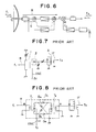
- a type of diode mixer which has been used in ordinary transmitters, radars, etc., involving frequencies higher than the ultra high frequency band.
- a signal R of a frequency f1 which has been received through a tuning circuit 1
- a local-oscillator signal OSC of a frequency f2 is coupled with a local-oscillator signal OSC of a frequency f2,mixed by a diode 2 and outputted as an intermediate frequency signal IF of a frequency f1 + f2 or
- Such diode mixers have large conversion loss and, frequently, coupling loss due to the inevitable use of magnetic coupling for the tuning circuit and thus restrictions are imposed on obtaining the best coupling.
- Fig. 8 shows a circuit diagram of the double balanced mixer.
- the double balanced mixer includes 4 diodes D1, D2, D3 and D4 which are connected in a ring form so that when, a receiving signal R is applied via an input-output transformer T1 and also a local-oscillator signal OSC is applied between the secondary side of the input-output transformer T1 and the primary side of an input-output transformer T2, an intermediate frequency signal IF of a frequency f1 + f2 or
- the double balanced mixer has been designed so that the local-oscillator signal OSC does not leak from the mixer circuit.
- the cross modulation distortion characteristic is excellent as compared with that of vacuum mixers, transistor mixers and diode mixers.
- the oupled circuit can be coupled directly and is therefore, at present, the best mixer.
- the double balanced mixer is used in a variety of circuits.
- double balanced mixers have the disadvantage that their electric characteristics are largely dependent on the characteristics of their component parts such as the diodes and transformers thus requiring careful selection of component parts depending on the frequency band used.
- the output of the local-oscillator signal is between 10 and 30 dbm.
- the output of the local-oscillator signal corresponds to the transmitted output in microwave, resulting in a high cost just for the circuit generating the local-oscillator signal.
- the double balanced mixers have the disadvantage that they are high in conversion loss compared with mixers of the other types thus requiring the provision of an amplifier on the output side.
- the present invention has been made with a view to overcoming the stated deficiencies in the prior art, and it is an object of the present invention to provide a frequency-conversion mixer which can be used in either concentrated constant circuits or distributed constant circuits and which is capable of reversible conversion.
- Fig. 1 is a circuit diagram of a frequency-conversion mixer according to an embodiment of the present invention.
- symbol J designates an input terminal to which is applied a receiving signal R of a frequency f1, H an input terminal to which is applied a local-oscillator signal OSC of a frequency f2, G a common terminal (usually connected to ground), I an output terminal for generating an intermediate frequency signal IF of the frequencies f1, f2, f1 + f2 and
- Fig. 2 shows the relation between the input and output signals in the frequency-conversion mixer shown in Fig. 1.
- the receiving signal R is applied to the terminal J and the local-oscillator signal OSC is applied to the terminal H, the intermediate frequency signal IF is produced from the terminal I.
- the local-oscillator signal OSC applied to the terminal H is subjected to non-linear detection by the diodes D3 and D4.
- the potential at a point P is maintained substantially at a value which is 1/2 of the local-oscillator signal OSC by the diodes D3 and D4.
- the receiving signal R applied to the terminal J is mixed with the local-oscillator signal OSC at the point P through the diodes D1 and D2. It is to be noted that the level of the local-oscillator signal OSC is sufficient even if it is below 0 dbm.
- the application of a reverse voltage produces a capacitance component between the cathode and anode of the diode.
- the capacitance is on the order of 0.2 to 1 pF.
- a capacitance of this order is an ideal value for a coupling capacitor in cases where the frequency f1 is higher than 50 MHz. Therefore, the receiving signal R is not practically attenuated and its passing loss is extremely small.
- the present invention has the effect of eliminating the occurrence of the phenomenon that the sensitivity of the ordinary diode mixer is deteriorated due to its dead zone to small signals and matching the impedance of an external circuit connected to the terminal J and the impedance of the point P.
- the intermediate frequency signal IF generated from the point P has the frequency components of f1 ,f2, f1 + f2 and
- the capacitor C1 removes the dc component from the intermediate frequency signal IF and outputs it.
- a filter 10 for passing the desired frequency component is connected to the terminal I. In this case, a filter with a low impedance input is connected.
- the frequency-conversion mixer incorporates the coupling capacitor C1 to take the form of a one-chip IC, it may also be formed by assembling individual components.
- the mixer may take the form of a one-chip IC to which, as, for example, a coupling capacitor C1 of below 50 MHz is externally attached.
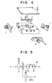
- the one-chip IC frequency-conversion mixer may be of a modular construction as shown in Fig. 4. By assembling the mixer as a module, there is the effect of making easy its fitting in a receiver as shown in Fig.5.
- the mixer in a receiver of the type employing the conventional diode mixer or double balanced mixer, it can be incorporated as such in place of the diode mixer or the double balanced mixer and it can be directly coupled to the tuning circuits.
- the manufacturing cost of the mixer circuit on the whole is substantially the same as the diode mixer or it is reduced to 1/10 as compared with the double balanced mixer as a single unit in an X-band radar. Further, the outputs of the high frequency amplifier and the local oscillator circuit amplifying unit can be reduced to thereby reduce the cost to substantially about 2/3.
- a signal S of a frequency f3 is applied to the terminal I instead of applying the receiving signal R of the frequency f1 to the terminal J as shown in Fig. 6, a signal of a frequency f2 ⁇ f3 is generated from the terminal J.
- the reversible conversion is permitted between the terminals J and I and the mixer can be applied to a reversible-conversion transmitting and receiving equipment.
- the frequency-conversion mixer in accordance with the present invention is small in size and low in conversion loss and requires no adjustment as compared with the conventional mixers such as the double balanced mixer requiring the use of input-output transformers.
- the frequency-conversion mixer according to the present invention can be used in a variety of equipment involving frequencies in the range of the low-frequency to the ultra-short frequency, e.g., as a satellite broadcasting receiver mixer, HF-SHF radio communication/transmitting and receiving mixer, microwave radar mixer, citizen's general radio, FM radio or television receiver mixer, spectrum analyzer mixer, heterodyne-type measuring instrument mixer, phase-locked loop oscillator mixer and phase discriminator.
- tuning circuit G common terminal (group) 2 diode H input terminal 3 tuning circuit I terminal (input) 10 filter IF intermediate frequency J terminal (for receiving signal) C1 capacitor, coupling D1 first diode OSC local oscillator signal D2 second diode R receiving signal D3 third diode P point D4 fourth diode S signal f - frequency T1 input-output transformer T2 input-output transformer
Landscapes
- Engineering & Computer Science (AREA)
- Power Engineering (AREA)
- Superheterodyne Receivers (AREA)
Claims (7)
- Ein frequenzumsetzender Mischer mit:Eingangsmitteln für den Empfang eines Signals, diese Eingangsmittel haben einen Anschluß (J) für den Empfang des Signals, einen Punkt (P) und erste und zweite antiparallel angeordnete Dioden (D1, D2) zwischen dem Anschluß (J) für den Empfang des Signals und dem Punkt (P),Detektiermitteln, die aufweisen eine Eingangsklemme (H) für das Signal eines lokalen Oszillators, einen gemeinsamen Anschluß (G) und dritte und vierte Dioden (D3, D4), die seriell in Durchlaß vom gemeinsamen Anschluß (G) zu der Eingangsklemme (H) für das Signal eines lokalen Oszillators geschaltet sind, wobei der Punkt (P) zwischen der dritten und der vierten Diode (D3, D4) angeschlossen ist, undeinem Kondensator (C1) für das Blockieren einer Gleichspannungskomponente, der an den Punkt (P) und eine Ausgangsklemme (I) angeschlossen ist.
- Frequenzumsetzender Mischer nach Anspruch 1, bei dem die Eingangsmittel und die Detektiermittel als monolithische integrierte Schaltung ausgeführt sind.
- Frequenzumsetzender Mischer nach Anspruch 1, bei dem die Eingangsmittel, die Detektiermittel und der Kondensator (C1) in Form einer monolithischen integrierten Schaltung ausgeführt sind.
- Frequenzumsetzender Mischer nach Anspruch 1, bei dem ein Signal einer ersten Frequenz den Eingangsmitteln zugeleitet wird und ein Signal einer zweiten Frequenz den Detektiermitteln zugeleitet wird.
- Frequenzumsetzender Mischer nach Anspruch 4, bei dem ein Signal einer Frequenz, die der Differenz oder Summe der ersten und der zweiten Frequenz entspricht, an der Ausgangsklemme (I) erzeugt wird.
- Frequenzumsetzender Mischer nach Anspruch 5, der weiterhin ein Filter aufweist, das an die Ausgangsklemme (I) angeschlossen ist und für den Durchlaß des Signals entweder der Differenz oder der Summe der ersten und der zweiten Frequenz ausgebildet ist.
- Frequenzumsetzender Mischer nach Anspruch 1, bei dem ein Signal einer zweiten Frequenz den Detektiermitteln zugeführt wird und ein Signal einer dritten Frequenz an der Ausgangsseite des Kondensators (C1) anliegt, wobei ein Signal einer Frequenz entsprechend der Differenz oder der Summe der zweiten und dritten Frequenz an den Eingangsmitteln erzeugt wird.
Priority Applications (1)
| Application Number | Priority Date | Filing Date | Title |
|---|---|---|---|
| DE1990626712 DE69026712T2 (de) | 1990-08-01 | 1990-08-01 | Frequenzumsetzender Mischer |
Applications Claiming Priority (1)
| Application Number | Priority Date | Filing Date | Title |
|---|---|---|---|
| JP1025857A JPH0744388B2 (ja) | 1989-02-06 | 1989-02-06 | 周波数変換ミクサ |
Publications (2)
| Publication Number | Publication Date |
|---|---|
| EP0469169A1 EP0469169A1 (de) | 1992-02-05 |
| EP0469169B1 true EP0469169B1 (de) | 1996-04-24 |
Family
ID=12177491
Family Applications (1)
| Application Number | Title | Priority Date | Filing Date |
|---|---|---|---|
| EP90114749A Expired - Lifetime EP0469169B1 (de) | 1989-02-06 | 1990-08-01 | Frequenzumsetzender Mischer |
Country Status (3)
| Country | Link |
|---|---|
| US (1) | US5212835A (de) |
| EP (1) | EP0469169B1 (de) |
| JP (1) | JPH0744388B2 (de) |
Families Citing this family (6)
| Publication number | Priority date | Publication date | Assignee | Title |
|---|---|---|---|---|
| FI89990C (fi) * | 1991-12-19 | 1993-12-10 | Nokia Mobile Phones Ltd | Diodblandare |
| DE4345242A1 (de) * | 1993-09-15 | 1995-04-06 | Endress Hauser Gmbh Co | Frequenzumsetzungsschaltung für ein Radar-Abstandsmeßgerät |
| JPH1056359A (ja) * | 1996-08-09 | 1998-02-24 | Alps Electric Co Ltd | デジタル放送受信チューナ |
| WO2007065639A1 (de) * | 2005-12-05 | 2007-06-14 | Vega Grieshaber Kg | Füllstandradarfrequenzumsetzer |
| DE102005058015B4 (de) | 2005-12-05 | 2015-12-03 | Vega Grieshaber Kg | Füllstandradarfrequenzumsetzer |
| JP2010057332A (ja) * | 2008-08-29 | 2010-03-11 | Dx Antenna Co Ltd | サージ保護回路及びこれを備えた高周波機器 |
Family Cites Families (3)
| Publication number | Priority date | Publication date | Assignee | Title |
|---|---|---|---|---|
| US3983489A (en) * | 1975-06-16 | 1976-09-28 | General Electric Company | Doubling mixer |
| JPS538005A (en) * | 1976-07-09 | 1978-01-25 | Matsushita Electric Ind Co Ltd | Frequency mixer |
| US4245355A (en) * | 1979-08-08 | 1981-01-13 | Eaton Corporation | Microwave frequency converter |
-
1989
- 1989-02-06 JP JP1025857A patent/JPH0744388B2/ja not_active Expired - Fee Related
-
1990
- 1990-07-18 US US07/554,731 patent/US5212835A/en not_active Expired - Lifetime
- 1990-08-01 EP EP90114749A patent/EP0469169B1/de not_active Expired - Lifetime
Also Published As
| Publication number | Publication date |
|---|---|
| EP0469169A1 (de) | 1992-02-05 |
| US5212835A (en) | 1993-05-18 |
| JPH02206205A (ja) | 1990-08-16 |
| JPH0744388B2 (ja) | 1995-05-15 |
Similar Documents
| Publication | Publication Date | Title |
|---|---|---|
| US4979233A (en) | High frequency broad-band mixing circuit including an electrolytic capacitor in parallel with a local oscillator input port | |
| US5361050A (en) | Balanced split ring resonator | |
| GB1476138A (en) | Tuner circuit arrangement | |
| US6810241B1 (en) | Microwave diode mixer | |
| EP1094597A1 (de) | Empfangsmodul und Empfänger | |
| US5521545A (en) | Collector-injection mixer with radio frequency signal applied to collectors of lower transistor pair | |
| US6661306B2 (en) | Compact lumped element dual highpass/lowpass balun layout | |
| US3983489A (en) | Doubling mixer | |
| US5212835A (en) | Frequency-conversion mixer | |
| EP0696870B1 (de) | Doppelt abgestimmte, frequenzbandumschaltbare HF-Schaltungsanordnung mit symmetrischen Ausgangssignalen | |
| HK75292A (en) | Circuit arrangement for an fm receiver | |
| US3458819A (en) | Uhf-if or vhf-if converter | |
| KR20240035468A (ko) | 트랜시버 드룹 교정 | |
| US4418320A (en) | High frequency discriminator with a crystal phase shift network | |
| KR100349704B1 (ko) | 더블 컨버젼 방식 튜너의 일차 밴드 패스 필터 | |
| FI92117C (fi) | Transistorisekoitin | |
| EP0201986A2 (de) | Intermodulationsunterdrückungsschaltung | |
| US5054118A (en) | Balanced mixer utilizing filters | |
| US4835492A (en) | Voltage controlled oscillator having constant tuning bias voltage | |
| EP0416889A2 (de) | Frequenzmischer | |
| US6675005B2 (en) | Printed single balanced downconverter mixer | |
| JPS622829Y2 (de) | ||
| KR900006075Y1 (ko) | 튜우너의 복동조를 이용한 if증폭기 | |
| KR100337081B1 (ko) | 디지털 튜너의 광대역 여파기 | |
| US20040053593A1 (en) | Signal mixers |
Legal Events
| Date | Code | Title | Description |
|---|---|---|---|
| PUAI | Public reference made under article 153(3) epc to a published international application that has entered the european phase |
Free format text: ORIGINAL CODE: 0009012 |
|
| 17P | Request for examination filed |
Effective date: 19910617 |
|
| AK | Designated contracting states |
Kind code of ref document: A1 Designated state(s): CH DE FR GB IT LI NL SE |
|
| 17Q | First examination report despatched |
Effective date: 19931102 |
|
| RIN1 | Information on inventor provided before grant (corrected) |
Inventor name: SUZUKI , EIJI |
|
| GRAH | Despatch of communication of intention to grant a patent |
Free format text: ORIGINAL CODE: EPIDOS IGRA |
|
| GRAA | (expected) grant |
Free format text: ORIGINAL CODE: 0009210 |
|
| AK | Designated contracting states |
Kind code of ref document: B1 Designated state(s): CH DE FR GB IT LI NL SE |
|
| REG | Reference to a national code |
Ref country code: CH Ref legal event code: NV Representative=s name: KIRKER & CIE SA |
|
| ITF | It: translation for a ep patent filed | ||
| REF | Corresponds to: |
Ref document number: 69026712 Country of ref document: DE Date of ref document: 19960530 |
|
| ET | Fr: translation filed | ||
| PLBE | No opposition filed within time limit |
Free format text: ORIGINAL CODE: 0009261 |
|
| STAA | Information on the status of an ep patent application or granted ep patent |
Free format text: STATUS: NO OPPOSITION FILED WITHIN TIME LIMIT |
|
| 26N | No opposition filed | ||
| K1C1 | Correction of patent application (title page) published |
Effective date: 19920205 |
|
| REG | Reference to a national code |
Ref country code: GB Ref legal event code: IF02 |
|
| PGFP | Annual fee paid to national office [announced via postgrant information from national office to epo] |
Ref country code: GB Payment date: 20040701 Year of fee payment: 15 |
|
| PGFP | Annual fee paid to national office [announced via postgrant information from national office to epo] |
Ref country code: FR Payment date: 20040709 Year of fee payment: 15 |
|
| PGFP | Annual fee paid to national office [announced via postgrant information from national office to epo] |
Ref country code: SE Payment date: 20040813 Year of fee payment: 15 |
|
| PGFP | Annual fee paid to national office [announced via postgrant information from national office to epo] |
Ref country code: NL Payment date: 20040827 Year of fee payment: 15 |
|
| PGFP | Annual fee paid to national office [announced via postgrant information from national office to epo] |
Ref country code: CH Payment date: 20041109 Year of fee payment: 15 |
|
| PGFP | Annual fee paid to national office [announced via postgrant information from national office to epo] |
Ref country code: DE Payment date: 20050202 Year of fee payment: 15 |
|
| PG25 | Lapsed in a contracting state [announced via postgrant information from national office to epo] |
Ref country code: IT Free format text: LAPSE BECAUSE OF NON-PAYMENT OF DUE FEES;WARNING: LAPSES OF ITALIAN PATENTS WITH EFFECTIVE DATE BEFORE 2007 MAY HAVE OCCURRED AT ANY TIME BEFORE 2007. THE CORRECT EFFECTIVE DATE MAY BE DIFFERENT FROM THE ONE RECORDED. Effective date: 20050801 Ref country code: GB Free format text: LAPSE BECAUSE OF NON-PAYMENT OF DUE FEES Effective date: 20050801 |
|
| PG25 | Lapsed in a contracting state [announced via postgrant information from national office to epo] |
Ref country code: SE Free format text: LAPSE BECAUSE OF NON-PAYMENT OF DUE FEES Effective date: 20050802 |
|
| PG25 | Lapsed in a contracting state [announced via postgrant information from national office to epo] |
Ref country code: LI Free format text: LAPSE BECAUSE OF NON-PAYMENT OF DUE FEES Effective date: 20050831 Ref country code: CH Free format text: LAPSE BECAUSE OF NON-PAYMENT OF DUE FEES Effective date: 20050831 |
|
| PG25 | Lapsed in a contracting state [announced via postgrant information from national office to epo] |
Ref country code: NL Free format text: LAPSE BECAUSE OF NON-PAYMENT OF DUE FEES Effective date: 20060301 Ref country code: DE Free format text: LAPSE BECAUSE OF NON-PAYMENT OF DUE FEES Effective date: 20060301 |
|
| REG | Reference to a national code |
Ref country code: CH Ref legal event code: PL |
|
| EUG | Se: european patent has lapsed | ||
| GBPC | Gb: european patent ceased through non-payment of renewal fee |
Effective date: 20050801 |
|
| PG25 | Lapsed in a contracting state [announced via postgrant information from national office to epo] |
Ref country code: FR Free format text: LAPSE BECAUSE OF NON-PAYMENT OF DUE FEES Effective date: 20060428 |
|
| NLV4 | Nl: lapsed or anulled due to non-payment of the annual fee |
Effective date: 20060301 |
|
| REG | Reference to a national code |
Ref country code: FR Ref legal event code: ST Effective date: 20060428 |