EP0469653A1 - Circuit intégré pourvu d'un ciruit-tampon d'entrée - Google Patents
Circuit intégré pourvu d'un ciruit-tampon d'entrée Download PDFInfo
- Publication number
- EP0469653A1 EP0469653A1 EP91201609A EP91201609A EP0469653A1 EP 0469653 A1 EP0469653 A1 EP 0469653A1 EP 91201609 A EP91201609 A EP 91201609A EP 91201609 A EP91201609 A EP 91201609A EP 0469653 A1 EP0469653 A1 EP 0469653A1
- Authority
- EP
- European Patent Office
- Prior art keywords
- signal
- input
- gate
- chip select
- input buffer
- Prior art date
- Legal status (The legal status is an assumption and is not a legal conclusion. Google has not performed a legal analysis and makes no representation as to the accuracy of the status listed.)
- Granted
Links
Images
Classifications
-
- G—PHYSICS
- G11—INFORMATION STORAGE
- G11C—STATIC STORES
- G11C7/00—Arrangements for writing information into, or reading information out from, a digital store
-
- G—PHYSICS
- G11—INFORMATION STORAGE
- G11C—STATIC STORES
- G11C8/00—Arrangements for selecting an address in a digital store
- G11C8/06—Address interface arrangements, e.g. address buffers
Definitions
- the invention relates to an integrated circuit including an input buffer circuit for generating an inverted and a non-inverted logic output signal in dependence on an input signal switching between a first and a second voltage, having a first and a second input gate, each having an input for receiving the input signal and an input for receiving a signal derived from a chip select signal, and each having an output for providing a first and a second intermediate signal, further including a first and a second amplifier circuit for converting the intermediate signals into the logic output signals.
- Such an integrated circuit is disclosed in the United States patent 4,807,198, which describes an integrated circuit in which the input signal and the chip select signal are applied to two input NOR gates, whose outputs are each connected via a hysteresis circuit to cross-wise coupled NAND gates, which form a latch.
- the two data paths thus formed have different switching points which cause, when the input signal increases or decreases, the output signal present to be deselected before the new output signal is selected.
- the different switching points of the data paths are realised by a suitable dimensioning of the relevant transistors of the input gates and hysteresis circuits. The process spread which is unavoidably caused during production results in unwanted inaccuracies.
- an integrated circuit according to the invention is characterized, in that, the first input gate is a NAND gate and the second input gate is a NOR gate, the input buffer circuit further including means for applying in the inverted form the chip select signal to the NOR-gate and for applying in the non-inverted form the chip select signal to the NAND gate.
- the invention is based on the recognition that with a substantially equal dimensioning of the transistors in CMOS a NAND gate has a higher switching point than a NOR gate. This is caused by the fact that the series-arranged n-channel transistors of a NAND gate provide a pull-down which is weaker than the pull-up provided by the p-channel transistors which are not arranged in series. For a NOR gate the opposite holds: the pull-down is stronger, so the switching point is lower. Thus, in a simple manner the necessity of a suitable dimensioning of a large number of transistors is obviated.
- an integrated circuit of the invention is characterized in that, it includes a further input buffer circuit whose input signal is an external chip select signal CSE and whose chip select signal is an external supply voltage field Vdd, the output of the further input buffer circuit being applied as the chip select signal to the input buffer circuit.
- the external chip select signal is converted into an internal (CMOS) chip select signal.
- an integrated circuit in accordance with the invention is characterized in that, it includes a memory circuit and has a plurality of input buffer circuits, the relevant input signals being address signals.
- a memory-IC it is advantageous that, by using the inverter before the NOR gate the capacitive load of the chip select signal is decreased, as a result of which this signal becomes faster.
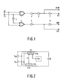
- an input signal AI is connected to a full CMOS NAND gate 1 and to a full CMOS NOR gate 2.
- the input signal AI is, for example, a TTL data or address signal, switching between, for example, 0.4 V (low) and 2.4 V (high), and which is to be converted into a CMOS data or address signal, having a high level of 5 V and a low level of 0 V.
- a chip select signal CS is connected, in the non-inverted state, to NAND gate 1 and in the inverted state to NOR gate 2, by means of a standard CMOS inverter 3.
- the chip select signal CS is a CMOS signal which reduces the current consumption when that portion of the integrated circuit to which the signal is applied, in this case the input buffer circuit, is not used.
- the output of NAND gate 1 is connected to inverter 5, whose output supplies an inverted address-transition-detection signal ATDB and is also connected to inverter 7, whose output supplies the output signal A0.
- the output of NOR gate 2 is connected to inverter 6, whose output supplies an address-transition-detection signal ATD and is also connected to inverter 8, whose output supplies the inverted output signal AOB.
- the inverters 4, 5 and 7 together form a first amplifier circuit which amplifies the intermediate signal supplied by the NAND gate into the non-inverted output signal A0, whilst the inverters 6 and 8 together form a second amplifier circuit which amplifies the intermediate signal supplied by NOR gate 2 into the inverted output signal AOB.
- the NAND gate 1 has a pull-up, because of its non-series arranged p-channel transistors, which is greater than the pull-down because of its series-arranged n-channel transistors.
- the NOR gate 2 has a pull-down, because of its non-series arranged n-channel transistors which is greater than the pull-up provided by its series-arranged p-channel transistors.
- NAND gate 1 has a higher switching point than NOR gate 2.
- AOB gets high.
- AI deselection again occurs first: AOB becomes low.
- AO becomes high.
- AO and AOB are temporarily both low.
- the speed of the chip select signal CS is important for a fast access of the integrated circuit portion driven thereby.
- both input gates are driven by signal CS, so that the signal CS is capacitively loaded twice.
- the inverter 3 precedes the NOR gate 2, which inverter capacitively loads the signal 5 to 10 times less than the load produced by the gates which were to be driven in the NOR gate 2 by signal CS.
- the signal CS is capacitively loaded to a far less extent and consequently becomes faster. Because of the choice of the number of inverters in the amplifier circuits the two paths through the input buffer circuit are of equal lengths in the signal CS.
- output signals AO and AOB are both low in response to a change in the input signal AI and also when the chip select signal CS is low. This fact can be utilized in the rest of the integrated circuit, since in an integrated circuit the same actions are often performed at a change in the input signal and at the deselection of a portion of the circuit (by changing CS to the low state).
- hysteresis circuits in the prior art input buffer circuit slow the circuit down and consume current.
- the transistors forming the circuit, in combination with the transistors of the input NOR gates must be suitably dimensioned to ensure the correct switching points.
- hysteresis circuits are superfluous because of the use of different switching points of the input gates.
- the input buffer circuit supplies ATD and ATDB signals for an address-transition-detection- circuit
- these signals may already be supplied at an earlier stage (more specifically after inverters 5 and 6) than the output signals (after inverters 7 and 8), since they need to be amplified to a less extent.
- ATD and ATDB become both temporarily high.
- chip select signal CS is low, ATD and ATDB both are temporarily switched to the high state. Also this fact can be utilized in the rest of the integrated circuit, for the same reasons as outlined above.
- FIG. 2 shows an integrated circuit including an input buffer circuit in accordance with the invention.
- Vdd and Vss are the external power supply terminals.
- the circuit includes a memory circuit MC and comprises several input buffer circuits, only one of which is shown for the sake of clarity: IPB.
- the input signals of the different input buffer circuits are address signals.
- AI is an external address signal, which in input buffer circuit IPB is converted into an internal address signal, which is further processed in the memory circuit MC.
- AE external output signal
- the conversion is effected under the control of internal chip select signal CS, which is, for example, generated from external chip select signal CSE by a further input buffer circuit CSB, of the same type as IPB, having input signals CSE instead of AI (at IPB) and Vdd instead of CS (at IPB).
- internal chip select signal CS which is, for example, generated from external chip select signal CSE by a further input buffer circuit CSB, of the same type as IPB, having input signals CSE instead of AI (at IPB) and Vdd instead of CS (at IPB).
Landscapes
- Engineering & Computer Science (AREA)
- Microelectronics & Electronic Packaging (AREA)
- Logic Circuits (AREA)
- Static Random-Access Memory (AREA)
- Semiconductor Integrated Circuits (AREA)
- Dram (AREA)
Applications Claiming Priority (2)
| Application Number | Priority Date | Filing Date | Title |
|---|---|---|---|
| NL9001500 | 1990-07-02 | ||
| NL9001500A NL9001500A (nl) | 1990-07-02 | 1990-07-02 | Geintegreerde schakeling voorzien van een invoer buffer schakeling. |
Publications (2)
| Publication Number | Publication Date |
|---|---|
| EP0469653A1 true EP0469653A1 (fr) | 1992-02-05 |
| EP0469653B1 EP0469653B1 (fr) | 1996-06-12 |
Family
ID=19857345
Family Applications (1)
| Application Number | Title | Priority Date | Filing Date |
|---|---|---|---|
| EP91201609A Expired - Lifetime EP0469653B1 (fr) | 1990-07-02 | 1991-06-24 | Circuit intégré pourvu d'un ciruit-tampon d'entrée |
Country Status (6)
| Country | Link |
|---|---|
| US (1) | US5157284A (fr) |
| EP (1) | EP0469653B1 (fr) |
| JP (1) | JP3169987B2 (fr) |
| KR (1) | KR100215165B1 (fr) |
| DE (1) | DE69120160T2 (fr) |
| NL (1) | NL9001500A (fr) |
Families Citing this family (15)
| Publication number | Priority date | Publication date | Assignee | Title |
|---|---|---|---|---|
| KR930008838A (ko) * | 1991-10-31 | 1993-05-22 | 김광호 | 어드레스 입력 버퍼 |
| US6043684A (en) * | 1995-12-20 | 2000-03-28 | Cypress Semiconductor Corp. | Method and apparatus for reducing skew between input signals and clock signals within an integrated circuit |
| US5903174A (en) * | 1995-12-20 | 1999-05-11 | Cypress Semiconductor Corp. | Method and apparatus for reducing skew among input signals within an integrated circuit |
| US6411140B1 (en) | 1995-12-20 | 2002-06-25 | Cypress Semiconductor Corporation | Method and apparatus for reducing skew between input signals and clock signals within an integrated circuit |
| US5835970A (en) * | 1995-12-21 | 1998-11-10 | Cypress Semiconductor Corp. | Burst address generator having two modes of operation employing a linear/nonlinear counter using decoded addresses |
| US6097222A (en) * | 1997-10-27 | 2000-08-01 | Cypress Semiconductor Corp. | Symmetrical NOR gates |
| US5889416A (en) * | 1997-10-27 | 1999-03-30 | Cypress Semiconductor Corporation | Symmetrical nand gates |
| US6278295B1 (en) | 1998-02-10 | 2001-08-21 | Cypress Semiconductor Corp. | Buffer with stable trip point |
| US6523614B2 (en) * | 2001-04-19 | 2003-02-25 | Halliburton Energy Services, Inc. | Subsurface safety valve lock out and communication tool and method for use of the same |
| JP2006512092A (ja) * | 2002-12-30 | 2006-04-13 | ザ・リージェンツ・オブ・ジ・ユニバーシティ・オブ・カリフォルニア | 病原体の検出および分析のための方法および装置 |
| US20050176532A1 (en) * | 2004-02-09 | 2005-08-11 | Thorington Andrew K. | Multiple performance game ball |
| US7799553B2 (en) | 2004-06-01 | 2010-09-21 | The Regents Of The University Of California | Microfabricated integrated DNA analysis system |
| US7766033B2 (en) * | 2006-03-22 | 2010-08-03 | The Regents Of The University Of California | Multiplexed latching valves for microfluidic devices and processors |
| US8841116B2 (en) | 2006-10-25 | 2014-09-23 | The Regents Of The University Of California | Inline-injection microdevice and microfabricated integrated DNA analysis system using same |
| WO2009015296A1 (fr) | 2007-07-24 | 2009-01-29 | The Regents Of The University Of California | Générateur de gouttelettes microfabriqué |
Citations (5)
| Publication number | Priority date | Publication date | Assignee | Title |
|---|---|---|---|---|
| US4630239A (en) * | 1985-07-01 | 1986-12-16 | Motorola, Inc. | Chip select speed-up circuit for a memory |
| GB2190558A (en) * | 1986-04-08 | 1987-11-18 | Nec Corp | Memory access control circuit |
| WO1988009037A1 (fr) * | 1987-05-04 | 1988-11-17 | Siemens Aktiengesellschaft | Memoire ram-cmos a agencement de circuits prediffuses |
| US4807198A (en) * | 1987-12-28 | 1989-02-21 | Motorola, Inc. | Memory input buffer with hysteresis and dc margin |
| US4907203A (en) * | 1987-11-19 | 1990-03-06 | Mitsubishi Denki Kabushiki Kaisha | Semiconductor memory device with changeable word organization modes including a test mode |
Family Cites Families (1)
| Publication number | Priority date | Publication date | Assignee | Title |
|---|---|---|---|---|
| JPH01140494A (ja) * | 1987-11-26 | 1989-06-01 | Mitsubishi Electric Corp | 半導体記憶装置の出力バッファ回路 |
-
1990
- 1990-07-02 NL NL9001500A patent/NL9001500A/nl not_active Application Discontinuation
-
1991
- 1991-06-24 EP EP91201609A patent/EP0469653B1/fr not_active Expired - Lifetime
- 1991-06-24 DE DE69120160T patent/DE69120160T2/de not_active Expired - Fee Related
- 1991-06-28 KR KR1019910010856A patent/KR100215165B1/ko not_active Expired - Fee Related
- 1991-07-01 US US07/724,099 patent/US5157284A/en not_active Expired - Fee Related
- 1991-07-01 JP JP18583691A patent/JP3169987B2/ja not_active Expired - Fee Related
Patent Citations (5)
| Publication number | Priority date | Publication date | Assignee | Title |
|---|---|---|---|---|
| US4630239A (en) * | 1985-07-01 | 1986-12-16 | Motorola, Inc. | Chip select speed-up circuit for a memory |
| GB2190558A (en) * | 1986-04-08 | 1987-11-18 | Nec Corp | Memory access control circuit |
| WO1988009037A1 (fr) * | 1987-05-04 | 1988-11-17 | Siemens Aktiengesellschaft | Memoire ram-cmos a agencement de circuits prediffuses |
| US4907203A (en) * | 1987-11-19 | 1990-03-06 | Mitsubishi Denki Kabushiki Kaisha | Semiconductor memory device with changeable word organization modes including a test mode |
| US4807198A (en) * | 1987-12-28 | 1989-02-21 | Motorola, Inc. | Memory input buffer with hysteresis and dc margin |
Also Published As
| Publication number | Publication date |
|---|---|
| JPH04229492A (ja) | 1992-08-18 |
| NL9001500A (nl) | 1992-02-03 |
| KR920003656A (ko) | 1992-02-29 |
| EP0469653B1 (fr) | 1996-06-12 |
| US5157284A (en) | 1992-10-20 |
| KR100215165B1 (ko) | 1999-08-16 |
| DE69120160T2 (de) | 1996-12-12 |
| DE69120160D1 (de) | 1996-07-18 |
| JP3169987B2 (ja) | 2001-05-28 |
Similar Documents
| Publication | Publication Date | Title |
|---|---|---|
| EP0469653B1 (fr) | Circuit intégré pourvu d'un ciruit-tampon d'entrée | |
| US5532620A (en) | Input buffer circuit capable of corresponding to variation of operating voltage in semiconductor integrated circuit | |
| US4616143A (en) | High voltage bootstrapping buffer circuit | |
| US4379974A (en) | Delay stage for a clock generator | |
| KR980011424A (ko) | 디지털 신호 전달 장치 | |
| EP0130910B1 (fr) | Amplificateur de lecture | |
| EP0328110A2 (fr) | Circuit de mise en fonction de mode pour mémoire DRAM | |
| US5295117A (en) | Semiconductor memory device and method for controlling an output buffer utilizing an address transition detector | |
| US4396845A (en) | Address buffer circuit | |
| US4894559A (en) | Buffer circuit operable with reduced power consumption | |
| US4970693A (en) | Semiconductor memory device with internal control signal based upon output timing | |
| EP0115140B1 (fr) | Circuit décodeur | |
| US5874853A (en) | Semiconductor integrated circuit system | |
| US5982220A (en) | High speed multiplexer circuit | |
| US6323685B1 (en) | Threshold voltage scalable buffer with reference level | |
| EP0458213B1 (fr) | Circuit de commande pour commander un mode d'opération dans une RAM pseudo-statique | |
| KR100311973B1 (ko) | 로직 인터페이스 회로 및 이를 이용한 반도체 메모리 장치 | |
| US6118325A (en) | Semiconductor device capable of preventing ringing of output waveform | |
| US6130558A (en) | Data transfer circuit and method for a semiconductor memory | |
| JPH027619A (ja) | インターフエイス回路 | |
| EP0030118B1 (fr) | Circuit décodeur | |
| US4641049A (en) | Timing signal generator | |
| US4902911A (en) | Semiconductor integrated circuit having a built-in power voltage generator | |
| EP0034465B1 (fr) | Circuit tampon d'adresses | |
| KR100358135B1 (ko) | 단일 위상 클럭을 이용한 프로그램가능 논리 어레이 |
Legal Events
| Date | Code | Title | Description |
|---|---|---|---|
| PUAI | Public reference made under article 153(3) epc to a published international application that has entered the european phase |
Free format text: ORIGINAL CODE: 0009012 |
|
| AK | Designated contracting states |
Kind code of ref document: A1 Designated state(s): DE FR GB IT |
|
| 17P | Request for examination filed |
Effective date: 19920727 |
|
| 17Q | First examination report despatched |
Effective date: 19950801 |
|
| GRAH | Despatch of communication of intention to grant a patent |
Free format text: ORIGINAL CODE: EPIDOS IGRA |
|
| GRAH | Despatch of communication of intention to grant a patent |
Free format text: ORIGINAL CODE: EPIDOS IGRA |
|
| GRAA | (expected) grant |
Free format text: ORIGINAL CODE: 0009210 |
|
| AK | Designated contracting states |
Kind code of ref document: B1 Designated state(s): DE FR GB IT |
|
| REF | Corresponds to: |
Ref document number: 69120160 Country of ref document: DE Date of ref document: 19960718 |
|
| ITF | It: translation for a ep patent filed | ||
| ET | Fr: translation filed | ||
| PLBE | No opposition filed within time limit |
Free format text: ORIGINAL CODE: 0009261 |
|
| STAA | Information on the status of an ep patent application or granted ep patent |
Free format text: STATUS: NO OPPOSITION FILED WITHIN TIME LIMIT |
|
| 26N | No opposition filed | ||
| REG | Reference to a national code |
Ref country code: FR Ref legal event code: CD |
|
| REG | Reference to a national code |
Ref country code: GB Ref legal event code: IF02 |
|
| PGFP | Annual fee paid to national office [announced via postgrant information from national office to epo] |
Ref country code: FR Payment date: 20020625 Year of fee payment: 12 |
|
| PGFP | Annual fee paid to national office [announced via postgrant information from national office to epo] |
Ref country code: GB Payment date: 20020628 Year of fee payment: 12 |
|
| PGFP | Annual fee paid to national office [announced via postgrant information from national office to epo] |
Ref country code: DE Payment date: 20020821 Year of fee payment: 12 |
|
| REG | Reference to a national code |
Ref country code: FR Ref legal event code: D6 |
|
| REG | Reference to a national code |
Ref country code: GB Ref legal event code: 746 Effective date: 20021111 |
|
| PG25 | Lapsed in a contracting state [announced via postgrant information from national office to epo] |
Ref country code: GB Free format text: LAPSE BECAUSE OF NON-PAYMENT OF DUE FEES Effective date: 20030624 |
|
| PG25 | Lapsed in a contracting state [announced via postgrant information from national office to epo] |
Ref country code: DE Free format text: LAPSE BECAUSE OF NON-PAYMENT OF DUE FEES Effective date: 20040101 |
|
| GBPC | Gb: european patent ceased through non-payment of renewal fee |
Effective date: 20030624 |
|
| PG25 | Lapsed in a contracting state [announced via postgrant information from national office to epo] |
Ref country code: FR Free format text: LAPSE BECAUSE OF NON-PAYMENT OF DUE FEES Effective date: 20040227 |
|
| REG | Reference to a national code |
Ref country code: FR Ref legal event code: ST |
|
| PG25 | Lapsed in a contracting state [announced via postgrant information from national office to epo] |
Ref country code: IT Free format text: LAPSE BECAUSE OF NON-PAYMENT OF DUE FEES Effective date: 20050624 |