EP0469821B1 - Schaltnetzteil - Google Patents
Schaltnetzteil Download PDFInfo
- Publication number
- EP0469821B1 EP0469821B1 EP91306914A EP91306914A EP0469821B1 EP 0469821 B1 EP0469821 B1 EP 0469821B1 EP 91306914 A EP91306914 A EP 91306914A EP 91306914 A EP91306914 A EP 91306914A EP 0469821 B1 EP0469821 B1 EP 0469821B1
- Authority
- EP
- European Patent Office
- Prior art keywords
- frequency
- khz
- frequencies
- signals
- power supply
- Prior art date
- Legal status (The legal status is an assumption and is not a legal conclusion. Google has not performed a legal analysis and makes no representation as to the accuracy of the status listed.)
- Expired - Lifetime
Links
- 230000001360 synchronised effect Effects 0.000 claims description 44
- 238000000034 method Methods 0.000 claims description 5
- 230000001105 regulatory effect Effects 0.000 claims description 5
- 238000007493 shaping process Methods 0.000 description 8
- 239000003990 capacitor Substances 0.000 description 4
- 230000001276 controlling effect Effects 0.000 description 4
- 238000009499 grossing Methods 0.000 description 4
- 238000010009 beating Methods 0.000 description 1
- 238000010586 diagram Methods 0.000 description 1
- 230000004907 flux Effects 0.000 description 1
- 230000000977 initiatory effect Effects 0.000 description 1
- 229910052760 oxygen Inorganic materials 0.000 description 1
- 229910052717 sulfur Inorganic materials 0.000 description 1
Images




Classifications
-
- H—ELECTRICITY
- H04—ELECTRIC COMMUNICATION TECHNIQUE
- H04N—PICTORIAL COMMUNICATION, e.g. TELEVISION
- H04N3/00—Scanning details of television systems; Combination thereof with generation of supply voltages
- H04N3/10—Scanning details of television systems; Combination thereof with generation of supply voltages by means not exclusively optical-mechanical
- H04N3/16—Scanning details of television systems; Combination thereof with generation of supply voltages by means not exclusively optical-mechanical by deflecting electron beam in cathode-ray tube, e.g. scanning corrections
- H04N3/18—Generation of supply voltages, in combination with electron beam deflecting
- H04N3/185—Maintaining DC voltage constant
-
- H—ELECTRICITY
- H02—GENERATION; CONVERSION OR DISTRIBUTION OF ELECTRIC POWER
- H02M—APPARATUS FOR CONVERSION BETWEEN AC AND AC, BETWEEN AC AND DC, OR BETWEEN DC AND DC, AND FOR USE WITH MAINS OR SIMILAR POWER SUPPLY SYSTEMS; CONVERSION OF DC OR AC INPUT POWER INTO SURGE OUTPUT POWER; CONTROL OR REGULATION THEREOF
- H02M3/00—Conversion of DC power input into DC power output
- H02M3/22—Conversion of DC power input into DC power output with intermediate conversion into AC
- H02M3/24—Conversion of DC power input into DC power output with intermediate conversion into AC by static converters
- H02M3/28—Conversion of DC power input into DC power output with intermediate conversion into AC by static converters using discharge tubes with control electrode or semiconductor devices with control electrode to produce the intermediate AC
- H02M3/325—Conversion of DC power input into DC power output with intermediate conversion into AC by static converters using discharge tubes with control electrode or semiconductor devices with control electrode to produce the intermediate AC using devices of a triode or a transistor type requiring continuous application of a control signal
- H02M3/335—Conversion of DC power input into DC power output with intermediate conversion into AC by static converters using discharge tubes with control electrode or semiconductor devices with control electrode to produce the intermediate AC using devices of a triode or a transistor type requiring continuous application of a control signal using semiconductor devices only
- H02M3/33507—Conversion of DC power input into DC power output with intermediate conversion into AC by static converters using discharge tubes with control electrode or semiconductor devices with control electrode to produce the intermediate AC using devices of a triode or a transistor type requiring continuous application of a control signal using semiconductor devices only with automatic control of the output voltage or current, e.g. flyback converters
Definitions
- the present invention relates to a switch mode power supply for a multi-frequency display system wherein plural horizontal synchronous pulse trains of different frequencies are used to support plural multi-display modes.
- a switch mode power supply is used to provide a stabilised DC power supply in a CRT display device for a personal computer workstation.
- Such power supplies are usually mounted within a space in the display device.
- this can produce objectionable problems, jitter or beating noise on the display because of interference between the frequency of the horizontal scan signal of the CRT display caused by a magnetic flux leakage from a transformer of the power supply.
- the horizontal deflection circuit of the CRT is magnetically separated from the power supply by a shield.
- the horizontal deflection frequency is synchronized to the switching frequency, as shown in "Switch mode power supply for CRT display," IBM Technical Disclosure Bulletin. Vol. 29, No. 9, February 1987, pp. 3921-3922.
- the switch mode power supply is normally run at a multiple of horizontal scan frequency.
- the switch mode power supply operate scan horizontal scan frequency.
- AFC automatic frequency control circuit
- Sync input synchronisation signals when integer multiples of the respective frequencies of the sync signal are within a pull-in range of a centre frequency of the oscillator, the drive signal, when locked to the sync signal, having a frequency which is an integer multiples of the frequency of the sync signal
- AFC automatic frequency control circuit
- switching regulator for generating one or more regulated power supply output voltages in response to the switching signal.
- Japanese patent application 63-294727 discloses a power supply in which inputs of first and second switching regulators are commonly connected to DC bulk voltage output of a rectifying and smoothing circuit.
- the second switching regulator operates at a switching frequency which is N times larger than or 1/N times smaller than switching frequency of the first switching regulator (N is integer larger than 1).
- Multi-frequency type CRT display devices can operate in plural display modes of different horizontal scan frequencies such as, 31 KHz, 48 KHz, etc. to support various character display modes.
- the horizontal scan frequencies and the switching frequency of the power supply device are independent from each other, and the shield for magnetically isolating both the circuits is used.
- the switching frequency of the power supply is synchronised to a multiple of horizontal scan frequency. The multiple is used to permit high efficiency and reduced size of the power supply.
- the switching frequency of the power supply is determined by the following typical circuit parameters. Core size of a switching transformer, switching speed range of a rectifying diode capacitance and size of a smoothing capacitor, and design of heat sink for circuit components.
- a switch mode power supply comprising: an automatic frequency control circuit (AFC) including an oscillator for generating first and second drive signals and a synchronous circuit for locking the first and second drive signals respectively to first and second input synchronisation (sync) signals when integer multiples of the respective frequencies of the first and second sync signals are within a pull-in range of a centre frequency of the oscillator, the first and second drive signals, when locked to the first and second sync signals, having frequencies which are integer multiples of the respective frequencies of the first and second sync signals; a drive circuit for generating first and second switching signals in response to the first and second drive signals respectively; and a switching regulator for generating one or more regulated power supply output voltages in response to the first and second switching signals; characterised in that the power supply comprises a control circuit for selecting, during a test period, the centre frequency of the oscillator such that, during subsequent operation of the power supply, the frequency range occupied by the first and second drive signals is narrower than the frequency
- this switch mode power supply can operate within a narrower range of frequencies, the selection of circuit parameters, such as transformer core size, diode switching speed, smoothing capacitor capacitance, and heatsink size, is simplified. Furthermore, because the narrower range of frequencies includes higher frequencies, this power supply offers a significant improvement in efficiency.
- a method for operating a switch mode power supply comprising: generating first and second drive signals using an oscillator; locking the first and second drive signals respectively to first and second input synchronisation (sync) signals when integer multiples of the respective frequencies of the first and second sync signals are within a pull-in range of a centre frequency of the oscillator, the first and second drive signals, when locked to the first and second sync signals, having frequencies which are integer multiples of the respective frequencies of the first and second sync signals; generating first and second switching signals in response to the first and second drive signals respectively; generating one or more regulated power supply output voltages in response to the first and second switching signals; and selecting, during a test period, the centre frequency of the oscillator such that, during subsequent operation of the power supply, the frequency range occupied by the first and second drive signals is narrower than the frequency range occupied by the first and second sync signals, by increasing the oscillator frequency through integer multiples of the frequencies of the first
- power supply apparatus comprising: first means for selectively generating at least two horizontal synchronous pulse trains of different frequencies; second means connected to said first means for generating a first switching pulse train of a frequency of which is N times as large as the frequency of horizontal synchronous pulse train (N is a positive integer) and second switching pulse train of a frequency which is M times as large as the frequency of the other horizontal synchronous pulse train (M is a positive integer), with said N and M being selected to provide the narrowest switching frequency range; and power supply means of switching regulator type connected to said second means, which operates in a switching frequency range defined by said first and second switching pulse trains.
- the first means is preferably a display control circuit which selectively generates the first horizontal synchronous pulse train of the first frequency and the second horizontal synchronous pulse train of second frequency.
- the second means preferably includes an oscillator circuit for generating sawtooth waveform of a predetermined frequency, and a synchronous circuit receiving said sawtooth waveform and one of said first and second horizontal synchronous pulse train to modify said predetermined frequency to frequency which is N times as large as the frequency of first horizontal synchronous pulse train or frequency which is M times as large as the frequency of the second horizontal synchronous pulse train.
- power supply apparatus comprising first means for selectively generating one of plural horizontal synchronous pulse trains of different frequencies; frequency decision means for responding to information which indicates said frequencies of plural horizontal synchronous pulse trains, to select the broadest frequency range into which all the plural horizontal synchronous pulse trains can be synchronized, and to decide a basic frequency included in said narrowest frequency range; second means operating at said basic frequency and responding to one of said frequencies of plural horizontal synchronous pulse trains to generate one of plural switching pulse trains which are equal to multiples of said frequencies of plural horizontal synchronous pulse trains, respectively; and power supply means of switching regulator type connected to said second means, which operates in a switching frequency range defined by said frequencies equal to said multiples.
- the frequency decision means preferably includes an oscillator circuit varying a frequency of sawtooth waveform, a synchronous circuit connected to said oscillator circuit and receiving one of said plural horizontal synchronous pulse trains of different frequencies, and a frequency detecting circuit connected to said oscillator circuit and said synchronous circuit for detecting plural sets of frequencies, each set of which includes lock start frequency, lock frequency and lock end frequency, as said frequency of sawtooth waveform is being varied.
- the frequency decision means includes a control device which controls to generate said plural sets of frequencies for each horizontal synchronous pulse train, and compares the sets of frequencies detected at said plural horizontal synchronous pulse train to select the broadest frequency range into which all the plural horizontal synchronous pulse trains can be synchronized.
- Figure 1 shows display apparatus comprising an example of a power supply of the present invention.
- a display control circuit 1 is included in a personal computer.
- the personal computer can operate in one of plural character display modes requiring, for example, 640 dots/one horizontal line, 1056 dots/one horizontal line, 1280 dots/one horizontal line.
- a multi scan frequency type CRT display device is connected to the personal computer for displaying the plural character display modes.
- the circuit blocks except the display control circuit 1 in Figure 1 represent the power supply of the present invention.
- the power supply is mounted in a space within the CRT display device together with a horizontal deflection circuits, a flyback transformer, and other analog circuit, not shown.
- the display control circuit 1 is designed to respond to a signal indicating one of character display modes to generate a horizontal sync pulse train of frequencies, such as 31 KHz, 38 KHz, 48 KHz or 64 KHz, vertical sync pulse trains, and video signals of characters or images to be displayed on the CRT display device.
- a horizontal sync pulse train of frequencies such as 31 KHz, 38 KHz, 48 KHz or 64 KHz, vertical sync pulse trains, and video signals of characters or images to be displayed on the CRT display device.
- the horizontal synchronous pulse train of the selected frequency is supplied to a waveform shaping circuit 2 through a line 11.
- the horizontal sync pulse train 35 on the line 11 is shown in Figure 2.
- the waveform shaping circuit 2 generates pulses 36 on line 12, as shown in Figure 2.
- An automatic frequency control circuit (AFC) 3 includes an oscillator circuit 3A and a synchronous circuit 3B.
- a sawtooth waveform of a predetermined frequency generated by the oscillator circuit 3A is modified to a sawtooth waveform 37 of a frequency which is equal to a multiple of the frequency of the horizontal sync pulse train applied to the synchronous circuit 3B.
- the synchronous circuit 3B generates a feedback signal on a line 13A to equalise lower half 37A of a positive-going portion of the sawtooth waveform 37, which is separated by a leading edge of the pulse 36, from an upper half 37B of the portion.
- the AFC 3 responds to the pulses 36 on the line 12 to lock or synchronize the frequency of the sawtooth waveform at the frequency of the horizontal synchronous pulse train, as shown by the wave form 37.
- a duty control circuit 7 receives the waveform 37 to generate pulse train 38, as shown in the Figure 2 on a line 16.
- a power control circuit 8 in a switching regulator 9 receives the pulses 38 on the line 16 and a feedback signal on line 17 to generate switching pulses on line 18.
- a switching element, such as a switching transistor, 19 is controlled by the pulses on line 18.
- the operation of the power control circuit 8, switching transistor 19, transformer 20, diode 21, capacitor 22, and resistors R1 and R2 is well known in the art.
- Circuit blocks 1, 2, 7 and 9 are also well known in the art. Circuit blocks 3, 4, 6 and 10 are connected between the waveform shaping circuit 2 and the duty control circuit 7 in accordance with the present invention.
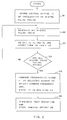
- the control device 10 positions switch 15 to position P1, and requests from the display control circuit 1 a list of the frequencies of horizontal sync (H-SYNC) pulse trains, i.e. 31 KHz, 38 KHz, 48 KHz and 64 KHz, supported by the display control circuit 1.
- the display control circuit 1 informs the control device 10 of the frequencies and these frequencies are stored in a register 6D, as shown by block 301 in Figure 3.
- control device 10 generates frequency values represented by the formulas; 31 KHz x K 38 KHz x K 48 KHz x K 64 KHz x K (wherein K is positive integer)
- the control device 10 stores the calculated values in a table 6A in the frequency detecting circuit 4, as shown in Figure 4.
- the control device 10 then causes the display control circuit 1 to generate Nth, i.e. the first 31 KHz in this case, horizontal synchronous pulse train on the line 11, and causes the variable frequency oscillator circuit 3A to generate the sawtooth waveform in the frequency range of 30 KHz - 280 KHz, for example.
- the sawtooth waveform the frequency of which is gradually increased from 30 KHz, is supplied to the synchronous circuit 3B through the line 13.
- the horizontal sync pulse train of 31 KHz is also supplied to the circuit 3B.
- the output of the AFC 3 is shown in Figure 5.
- the AFC 3 synchronizes its oscillating frequency to 62 KHz which is twice the horizontal scan frequency.
- the output frequency of the AFC 3 is locked to 62 KHz since the pull-in range in this example is set to ⁇ 5 KHz.
- the output frequency is released before 67 KHz.
- the 57 KHz frequency is called a lock start frequency F S
- the 62 KHz frequency is called as a lock frequency F L
- the 67 KHz frequency is called a lock end frequency F E .
- the frequency locks at 93 KHz, 124 KHz, 155 KHz, 186 KHz, 217 KHz and 248 KHz, as shown in the Figure 5.
- the frequencies F S , F L and F E for each locked frequency are detected by the frequency detecting circuit 4 and are supplied to the control device 10, which stores them in table 6B, as shown in Figure 6.
- the operation proceeds to block 304 in Figure 3, wherein the control device 10 checks as to whether or not all the frequencies of the horizontal synchronous pulse train have been tested. If not, the operation is returned to block 302 wherein the control device 10 causes the display control circuit 1 to generate the second horizontal scan frequency 38 KHz.
- the frequencies F S , F L and F E are detected by the frequency detecting circuit 4 and the detected values are stored in the table 6B, as shown in the Figure 6. In this manner, the frequencies F S , F L and F E for the horizontal synchronous frequencies 48 KHz and 64 KHz are detected and stored in the table 6B.
- the control device 10 selects a group of values corresponding to the horizontal scan frequencies 31 KHz, 38 KHz, 48 KHz and 64 KHz, and compares corresponding groups of lock start and end frequencies F S and to detect a common or basic frequency in the selected group.
- the control device 10 initially selects values A, B, C and D as the first group and compares the corresponding lock end frequencies 67 KHz, 81 KHz, 101 KHz and 133 KHz to select the lowest lock end frequency 67 KHz, then, the corresponding lock start frequencies 57 KHz, 71 KHz, 91 KHz and 123 KHz are compared to select the highest lock start frequency 123 KHz.
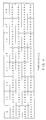
- the difference produced by subtracting the maximum lock start frequency (F S max) 123 KHz from the minimum lock end frequency (F E min) 67 KHz, -56KHz, is stored in frequency range 1 of table 6C in Figure 7.
- Control device 10 selects the values E, B, C and D as the second group and compares the corresponding lock end frequencies 98 KHz, 81 KHz, 101 KHz and 133 KHz to select the lowest lock end frequency 81 KHz;
- the corresponding lock start frequencies 88 KHz, 71 KHz, 91 KHz and 123 KHz are compared to to select the highest lock start frequency 123 KHz.
- the value - 42 KHz 81 KHz (F E min) - 123 KHz (F S max) is stored in range 2 of the Table 6C shown in Figure 7.
- Control device 10 selects the values E, F, C and D as the third group and compares the corresponding lock end frequencies 98 KHz, 119 KHz, 101 KHz and 133 KHz to select the lowest lock end frequency 98 KHz.
- the corresponding lock start frequencies 88 KHz, 109 KHz, 91 KHz and 123 KHz are compared to select the highest lock start frequency 123 KHz;
- the value -25 KHz, between the lowest lock end frequency 98 KHz and the highest lock start frequency 123 KHz is stored in range 3 table 6C in the Figure 7.
- Range 4 22 KHz: Values G, F, C and D Range 5 (-20 KHz): Values G, F, I and D Range 6 (-18 KHz): Values G, H, I and D Range 7 (-17 KHz): Values J, H, I and D Range 8 (-27 KHz): Values J, L, M and N Range 9 (+4 KHz) : Values K, L, M and N Range 10 (-70 KHz): Values K, P. Q and R Range 11 (-29 KHz): Values O, P, Q and R Range 12 (-18 KHz): Values S, P, Q and R
- Control device 10 compares the values of the frequency ranges 1 through 12 in the table 6C in the Figure 7 and selects the range 9 which has the positive maximum value 4 KHz.
- the broadest range 9 in this case includes the frequencies from 187 KHz to 191 KHz.
- the common lock frequency exists where condition F E min - F S max > 0 is satisfied.
- the control device 10 selects an intermediate frequency 189 KHz in the range 9 as the basic frequency of the broadest range 9, and stores the frequency 189 KHz in a register 6E.
- the basic frequency 189 KHz can be locked or synchronized to the multiples of all the horizontal scan frequencies in range 9. That is, the AFC 3 can synchronize to the multiples of all the horizontal scan frequencies in the range 9.
- control device 10 uses the common or basic frequency, i.e. 189 KHz, stored in register 6E shown in the Figure 1 to control the frequency of the oscillator circuit 3A.
- the frequency of the oscillator circuit 3A is fixed to the basic frequency 189 KHz in normal operation.
- the frequency 189 KHz is modified to synchronize to the multiples of the horizontal scan frequencies.
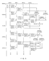
- Figure 8 shows the sawtooth waveform 81 of the basic frequency 189 KHz generated by the oscillator circuit 3A and applied to the synchronous circuit 3B, and various sawtooth waveforms of the frequencies shifted or modified from the 189 KHz depending upon the frequency of the horizontal scan pulse train, i.e. 31 KHz, 38 KHz, 48 KHz or 64 KHz, applied from the display control circuit 1 to the waveform shaping circuit 2.
- H-SYNC horizontal sync
- the sawtooth waveform 82 of the frequency 190 KHz is supplied to the duty control circuit 7 through the switch 15 in the position P2.
- the duty control circuit 7 and the power control circuit 8 generate the switching pulses 39, as shown in the Figure 2, of the frequency 190 KHz for controlling the switching transistor 19 of the switching regulators.
- the sawtooth waveform 84 of the frequency 186 KHz is supplied to the duty control circuit 7 through the switch 15 in the position P2.
- the duty control circuit 7 and the power control circuit 8 generate the switching pulses of the frequency 186 KHz for controlling the switching transistor 19 of the switching regulators.
- the sawtooth waveform 86 of the frequency 192 KHz is supplied to the duty control circuit 7 through the switch 15 in the position P2.
- the duty control circuit 7 and the power control circuit 8 generate the switching pulses of the frequency 192 KHz for controlling the switching transistor 19 of the switching regulator.
- the sawtooth waveform 86 of the frequency 192 KHz is supplied to the duty control circuit 7 through the switch 15 in the position P2.
- the duty control circuit 7 and the power control circuit 8 generate the switching pulses of the frequency 192 KHz for controlling the switching transistor 19 of the switching regulator.
- the embodiment of the power supply apparatus of the present invention hereinbefore described generates switching pulses of 186 KHz in response to a horizontal sync pulse train of 31 KHz, switching pulses of 190 KHz in response to a horizontal sync pulse train of 38 KHz, and switching pulses of 192 KHz in response to horizontal sync pulse trains of 48 KHz and 64 KHz, respectively.
- the multiplier 6 for the 31 KHz, 5 for the 38 KHz, 4 for the 48 KHz, and 3 for the 64 KHz are selected to provide the narrowest switching frequency range, i.e. the 6 KHz range. Selection of the switching frequency range is performed by block 305 in Figure 3.
- a basic frequency 153.5 KHz is selected, and modified to 155 KHz for 31 KHz and 152 KHz for 38 KHz.
- the basic frequency 153.5 KHz is stored in the register 6E as the frequency used for this particular combination of the horizontal sync pulse trains.
- the broadest range 9 is selected to give a large tolerance against the shift of the basic frequency due to the influence of temperature variation. This remarkably increases the stability of the power supply
- the frequencies, for example, 31 KHz, 38 KHz, 48 KHz and 64 KHz of the horizontal sync pulse trains are stored in the register 6D in the initial set-up period, and the basic frequency 189 KHz for this particular combination of the horizontal sync pulse trains is selected and stored in the register 6E.
- the basic frequency is selected depending upon the combination of the horizontal scan frequencies. Therefore, the control device 10 determined in each initial set-up period whether the frequencies of the horizontal sync pulse trains from the display control circuit 1 are equal to the frequencies stored in the register 6D. For example, suppose the frequencies stored in the register 6D are 31 KHz, 38 KHz, 48 KHz and 64 KHz, the frequency in the register 6E is 189 KHz, and a newly connected display control circuit 1 generates 31 KHz and 38 KHz, as described above. In this case, the old combination of 31 KHz, 38 KHz, 48 KHz and 64 KHz differs from the new combination of 31 KHz and 38 KHz.
- the control device 10 therefore, resets the old values in the registers 6D and 6E, and initiates the test operation shown in the Figure 3 to find out the new value 153.5 KHz for the new combination of 31 KHz and 38 KHz.
- the old value, 189 KHz in the register 6E is replaced by the new value, 153.5 KHz, and the old values 31 KHz, 38 KHz, 48 KHz and 64 KHz in the register 6D are replaced by the new values 31 KHz and 38 KHz.
- the control device 10 determines in the initial set-up period whether the frequencies of the horizontal synchronous pulse trains from the display control circuit 1 are equal to the frequencies stored in the register 6D. If they are, the control device 10 uses the frequency stored in the register 6E as the basic frequency without initiating the new test operation. Otherwise, the control device 10 resets the values in the registers 6D and 6E, and initiates the test operation to find out the new basic frequency for the new combination of the horizontal synchronous frequencies.
- an embodiment of the frequency detecting circuit 4 includes a comparing circuit 41, a register 42, gates 43 and 44 and a logic circuit 45.
- the oscillator circuit 3A gradually increases the frequency of the sawtooth waveform on the line 13 in the test period, as described hereinbefore.
- the oscillator circuit 3A also supplies a signal indicating the frequency to register 42 through a line 46.
- the frequency of the sawtooth waveform on the output line 14 of the AFC 3 is locked to 62 KHz. This locked condition is detected by comparing circuit 41.
- the multiples 62 KHz, 93 KHz, 124 KHz, 155 KHz, 186 KHz, 217 KHz and 248 KHz of 31 KHz stored in the Table 6A of Figure 4 are sequentially compared with the output frequency on the line 14 from the AFC 3.
- the comparing circuit 41 When the output frequency is equal to 62 KHz, the comparing circuit 41 generates a gate pulse on a line 47.
- the register 42 now stores a history frequency, such as 57 KHz in this case.
- the frequency 62 KHz is also supplied to the gate 43 through a line 48.
- Both the lock start frequency (F S ) 57 KHz and lock frequency (F L ) 62 KHz are supplied to the logic circuit 45 by the gate pulse on the line 47.
- the same operation as that described above is performed when the frequency of the oscillator circuit 3A exceeds each of the lock start frequencies (F S ) 88 KHz, 119 KHz, 150 KHz, 181 KHz, 212 KHz and 243 KHz, respectively, and Table 6B in Figure 6 is completed.
- a power supply of the present invention can be operated at multiples of plural horizontal scan frequencies, and also be synchronized to the plural horizontal scan frequencies.
- the operational range of the connected switching regulator can be minimized.
- circuit parameters, hereinbefore described can therefore easily be selected to optimize the power supply performance for a range of horizontal scan frequencies.
- the total efficiency of the power supply can be remarkably improved.
- its size can be reduced because the switching frequency is relatively high.
Landscapes
- Engineering & Computer Science (AREA)
- Multimedia (AREA)
- Signal Processing (AREA)
- Power Engineering (AREA)
- Television Receiver Circuits (AREA)
- Dc-Dc Converters (AREA)
Claims (8)
- Ein Schaltnetzteil enthaltend:
Einen automatischen Frequenzregelungsschaltkreis (AFC 3) einschließlich eines Oszillators (3a) zum Generieren eines ersten und eines zweiten Steuersignals, und einen synchronen Schaltkreis (3b) zum Synchronisieren des ersten bzw. des zweiten Steuersignals mit einem ersten bzw. einem zweiten Eingangssynchronisations-Signals, wenn ganzzahlige Vielfache der entsprechenden Frequenzen des ersten bzw. des zweiten Synchronisationssignals innerhalb des Ansprechbereichs einer Mittenfrequenz des Oszillators (3a) liegen; wobei das erste bez. das zweite Steuersignal, wenn sie mit dem ersten bzw. dem zweiten Synchronisationssignal synchron sind, Frequenzen aufweisen, die ganzzahlige Vielfache der entsprechenden Frequenzen des ersten bzw. des zweiten Sync-Signals sind;
eine Steuerschaltung (7) zum Generieren eines ersten bzw. eines zweiten Schaltsignals als Reaktion auf das erste bzw. das zweite Steuersignal; und
einen Schaltregler (9) zum Generieren einer oder mehrerer geregelter Netzteilausgangsspannungen als Reaktion auf dieses erste bzw. zweite Schaltsignal;
dadurch gekennzeichnet, daß das Netzteil einen Steuerkreis (4, 6, 10, 15) zum Anwählen der Mittenfrequenz des Oszillators (3a) während einer Testperiode aufweist, so daß während des nachfolgenden Betriebs des Netzteils der vom ersten und vom zweiten Steuersignal besetzte Frequenzbereich enger ist als der vom ersten und vom zweiten Synchronisationssignal besetzte Frequenzbereich; wobei der Steuerschaltkreis (4, 6, 10) beinhaltet:
Mittel zum Erhöhen der Oszillatorfrequenz durch ganzzahlige Vielfache der Frequenzen des ersten und des zweiten Synchronisationssignals;
einen Frequenzerfassungsschaltkreis (4) zum Festlegen der Startfrequenzen, bei denen die automatische Frequenzregelungsschaltung (AFC 3) sich mit dem ersten und dem zweiten Synchronisationssignal synchronisiert, wenn sich die Oszillatorfrequenz erhöht;
Mittel (6A, 6D, 10) zum Festlegen der Endfrequenzen, bei denen die automatische Frequenzregelungsschaltung (AFC 3) sich aus dem ersten und dem zweiten Synchronisationssignal ausklinkt, wenn sich die Oszillatorfrequenz erhöht;
Mittel (6B, 10) zum Auswählen unterschiedlicher Frequenzgruppen, die jeweils vorgegebene Start- und Endfrequenzen entsprechend dem ersten und dem zweiten Synchronisationssignal enthalten; Mittel (6B, 10) zum Bestimmen der niedrigsten Endfrequenz und der höchsten Startfrequenz in jeder Gruppe;
Mittel (10) zum Abziehen der höchsten Startfrequenz von der niedrigsten Endfrequenz in jeder Gruppe, um einen entsprechenden Frequenzbereich in jeder Gruppe zu generieren;
Mittel (6C, 10) zum Festlegen des breitesten positiven Bereichs aus den generierten Frequenzbereichen; und
Mittel (6D, 10) zum Einstellen der Mittenfrequenz des Oszillators auf die Zwischenfrequenz zwischen der niedrigsten Endfrequenz und der höchsten Startfrequenz entsprechend dem breitesten positiven Bereich. - Ein Netzteil gemäß Anspruch 1, in dem die Steuerschaltung (4, 6, 10, 15) ein erstes Register (6D) zum Abspeichern der Frequenzen des ersten und des zweiten Synchronisationssignals aus einer Synchronisationssignalquelle (1) aufweist.
- Ein Netzgerät gemäß Anspruch 2, in dem die Steuerschaltung (4, 6, 10, 15) Rückstellmittel (6D, 10) enthält zum Vergleichen neuer Frequenzen entsprechend dem ersten und dem zweiten Synchronisationssignal aus der Quelle mit den laufenden Frequenzen, die im ersten Register (6A) abgespeichert sind, während der Testperiode, und zum Ersetzen der laufenden, im ersten Register (6A) abgespeicherten Frequenzen durch die neuen Frequenzen, falls sich diese neuen Frequenzen von den laufenden Frequenzen unterscheiden.
- Ein Netzgerät gemäß einem beliebigen der vorstehenden Ansprüche, in dem die Steuerschaltung (4, 6, 10, 15) einen Schalter (15) aufweist, der ursprünglich den Ausgang der automatischen Frequenzsteuerschaltung (AFC 3) mit der Frequenzerfassungsschaltung verbindet und anschließend den Ausgang der automatischen Frequenzsteuerschaltung (AFC 3) mit der Antriebsschaltung (7) verbindet.
- Ein Netzgerät gemäß einem beliebigen der vorstehenden Ansprüche, in dem die Steuerschaltung (4, 6, 10, 15) eine erste Tabelle (6A) aufweist, um die ganzzahligen Vielfachen der Frequenzen des ersten und des zweiten Synchronisationssignals abzuspeichern.
- Ein Netzgerät gemäß einem beliebigen der vorstehenden Ansprüche, in dem die Steuerschaltung (4, 6, 10, 15) eine zweite Tabelle (6B), um die Startfrequenz und die Endfrequenz für das erste und das zweite Synchronisationssignal abzuspeichern; eine dritte Tabelle (6C), um den jeder Gruppe entsprechenden Bereich abzuspeichern; und ein zweites Register (6D) zum Abspeichern der Zwischenfrequenz in der Mitte zwischen der niedrigsten Endfrequenz und der höchsten Startfrequenz entsprechend dem breitesten positiven Bereich abzuspeichern, enthält.
- Eine Anzeigevorrichtung, enthaltend ein Schaltnetzteil gemäß einem beliebigen der vorstehenden Ansprüche, wobei das erste und das zweite Synchronisationssignal horizontale Bildsynchronisationssignale sind.
- Ein Verfahren zum Betreiben eines Schaltnetzteils, wobei dieses Verfahren beinhaltet:
Das Generieren eines ersten und eines zweiten Steuersignals durch Einsatz eines Oszillators (3a);
Synchronisieren des ersten und des zweiten Steuersignals entsprechend mit einem ersten bzw. einem zweiten Eingangs-Synchronisationssignal, sobald ganzzahlige Vielfache der entsprechenden Frequenzen des ersten bzw. des zweiten Sync-Signals innerhalb des Ansprechbereichs einer Mittenfrequenz des Oszillators (3a) liegen, wobei das erste und das zweite Steuersignal, wenn sie synchron mit dem ersten bzw. dem zweiten Synchronisationssignal laufen, Frequenzen aufweisen, die ganzzahlige Vielfache der entsprechenden Frequenzen des ersten bzw. des zweiten Synchronisationssignals sind;
Generieren eines ersten und eines zweiten Schaltsignals als Reaktion auf das erste bzw. das zweite Steuersignal;
Generieren einer oder mehrerer geregelter Netzteilausgangsspannungen als Reaktion auf das erste bzw. das zweite Schaltsignal;
wobei das verfahren gekennzeichnet ist durch
Wählen der Mittenfrequenz des Oszillators (3a) während einer Testperiode so, daß während des nachfolgenden Betriebs des Netzteils der vom ersten und zweiten Steuersignal besetzte Frequenzbereich enger als der vom ersten und vom zweiten Synchronisationssignal besetzte Frequenzbereich;
Erhöhen der Oszillatorfrequenz um ganzzahlige Vielfache der Frequenzen des ersten und des zweiten Synchronisationssignals,
Festlegen der Startfrequenzen, an denen sich das erste und das zweite Steuersignal mit dem ersten und dem zweiten Synchronisationssignal synchronisiert, wenn sich die Oszillatorfrequenz erhöht;
Festlegen der Endfrequenzen, an denen das erste und das zweite Steuersignal sich vom ersten und zweiten Synchronisationssignal ausklinkt, wenn die Oszillatorfrequenz zunimmt;
Auswählen unterschiedlicher Gruppen, die jeweils bestimmte Start- und Endfrequenzen enthalten, die dem ersten bzw. dem zweiten Synchronisationssignal entsprechen;
Festlegen der untersten Endfrequenz und der höchsten Startfrequenz in jeder Gruppe;
Abziehen der höchsten Startfrequenz von der niedrigsten Endfrequenz in jeder Gruppe, um einen den einzelnen Gruppen entsprechenden Frequenzbereich zu generieren;
Festlegen des breitesten Bereichs aus den generierten Frequenzbereichen; und
Einstellen der Mittenfrequenz des Oszillators (3a) auf die Zwischenfrequenz zwischen der niedrigsten Endfrequenz und der höchsten Startfrequenz, die dem breitesten positiven Bereich entspricht.
Applications Claiming Priority (2)
| Application Number | Priority Date | Filing Date | Title |
|---|---|---|---|
| JP205273/90 | 1990-08-03 | ||
| JP2205273A JPH0769670B2 (ja) | 1990-08-03 | 1990-08-03 | 電源装置 |
Publications (3)
| Publication Number | Publication Date |
|---|---|
| EP0469821A2 EP0469821A2 (de) | 1992-02-05 |
| EP0469821A3 EP0469821A3 (en) | 1992-05-06 |
| EP0469821B1 true EP0469821B1 (de) | 1994-11-30 |
Family
ID=16504247
Family Applications (1)
| Application Number | Title | Priority Date | Filing Date |
|---|---|---|---|
| EP91306914A Expired - Lifetime EP0469821B1 (de) | 1990-08-03 | 1991-07-29 | Schaltnetzteil |
Country Status (4)
| Country | Link |
|---|---|
| US (1) | US5132891A (de) |
| EP (1) | EP0469821B1 (de) |
| JP (1) | JPH0769670B2 (de) |
| DE (1) | DE69105400T2 (de) |
Families Citing this family (15)
| Publication number | Priority date | Publication date | Assignee | Title |
|---|---|---|---|---|
| US5438245A (en) * | 1992-05-27 | 1995-08-01 | Sony Corporation | High-voltage generating circuit |
| KR970003439B1 (ko) * | 1994-05-19 | 1997-03-18 | 삼성전자 주식회사 | 모니터의 전원 제어회로 |
| US5721506A (en) * | 1994-12-14 | 1998-02-24 | Micron Technology, Inc. | Efficient Vccp supply with regulation for voltage control |
| US5940147A (en) * | 1995-06-01 | 1999-08-17 | U.S. Philips Corporation | Power supply synchronization |
| US5841313A (en) * | 1995-08-30 | 1998-11-24 | Cherry Semiconductor Corporation | Switch with programmable delay |
| US6111451A (en) * | 1997-05-19 | 2000-08-29 | Micron Technology, Inc. | Efficient VCCP supply with regulation for voltage control |
| KR100219659B1 (ko) * | 1997-08-27 | 1999-09-01 | 윤종용 | 인쇄기용 전원공급제어장치 |
| DE19859538A1 (de) * | 1997-12-26 | 1999-07-08 | Ricoh Kk | Energiezufuhreinrichtung bzw. Netzteil und Verfahren für ein elektrofotografisches Gerät |
| DE19912627A1 (de) * | 1999-03-20 | 2000-09-28 | Thomson Brandt Gmbh | Schaltung zur Stabilisierung einer Hochspannung |
| KR100471058B1 (ko) * | 2001-10-23 | 2005-03-08 | 삼성전자주식회사 | 디스플레이장치 |
| AU2003233098A1 (en) * | 2002-06-18 | 2003-12-31 | Koninklijke Philips Electronics N.V. | Control circuit and method for controlling an electrical signal over a load such as a deflection circuit of a cathode ray tube |
| US20040090802A1 (en) * | 2002-11-01 | 2004-05-13 | Sierra Wireless, Inc., A Canadian Corporation | Noise suppression in switching power supplies |
| JP2004357645A (ja) * | 2003-06-09 | 2004-12-24 | Daisen Sangyo:Kk | 包装済みコンニャク |
| DE10329829A1 (de) * | 2003-07-02 | 2005-01-20 | Deutsche Thomson-Brandt Gmbh | Schaltnetzteil mit Synchronisierung |
| US7728571B2 (en) * | 2007-11-06 | 2010-06-01 | Richtek Technology Corporation, R.O.C. | Load-dependent frequency jittering circuit and load-dependent frequency jittering method |
Family Cites Families (7)
| Publication number | Priority date | Publication date | Assignee | Title |
|---|---|---|---|---|
| US3706023A (en) * | 1969-10-03 | 1972-12-12 | Tokyo Shibaura Electric Co | High voltage regulation circuit for television receiver |
| JPS52100929A (en) * | 1976-02-20 | 1977-08-24 | Hitachi Ltd | High-voltage protection circuit of tv receiver |
| US4524411A (en) * | 1982-09-29 | 1985-06-18 | Rca Corporation | Regulated power supply circuit |
| US4516168A (en) * | 1982-11-30 | 1985-05-07 | Rca Corporation | Shutdown circuit for a switching regulator in a remote controlled television receiver |
| US4692852A (en) * | 1986-06-25 | 1987-09-08 | Rca Corporation | Switching power supply with raster width stabilization |
| JPH01189284A (ja) * | 1988-01-22 | 1989-07-28 | Fujitsu Ltd | 同期分離回路 |
| JPH0721699B2 (ja) * | 1988-04-21 | 1995-03-08 | 株式会社日立製作所 | Crtモニタの電源回路 |
-
1990
- 1990-08-03 JP JP2205273A patent/JPH0769670B2/ja not_active Expired - Lifetime
-
1991
- 1991-06-27 US US07/722,462 patent/US5132891A/en not_active Expired - Fee Related
- 1991-07-29 DE DE69105400T patent/DE69105400T2/de not_active Expired - Fee Related
- 1991-07-29 EP EP91306914A patent/EP0469821B1/de not_active Expired - Lifetime
Also Published As
| Publication number | Publication date |
|---|---|
| DE69105400T2 (de) | 1995-06-08 |
| EP0469821A2 (de) | 1992-02-05 |
| DE69105400D1 (de) | 1995-01-12 |
| JPH0491579A (ja) | 1992-03-25 |
| EP0469821A3 (en) | 1992-05-06 |
| JPH0769670B2 (ja) | 1995-07-31 |
| US5132891A (en) | 1992-07-21 |
Similar Documents
| Publication | Publication Date | Title |
|---|---|---|
| EP0469821A2 (de) | Schaltnetzteil | |
| KR200204617Y1 (ko) | Lcd모니터의 수직화면 제어장치 | |
| US6285402B1 (en) | Device and method for converting scanning | |
| US4837457A (en) | High voltage power transistor circuits | |
| KR880000908B1 (ko) | 이중모드(mode) 수평 편향회로 | |
| US4623925A (en) | Television receiver having character generator with non-line locked clock oscillator | |
| KR100376631B1 (ko) | 동기화장치및동기화방법 | |
| KR100379313B1 (ko) | 동기주사회로 | |
| US5179331A (en) | Pulse width regulated high voltage power supply using ringless flyback transformer | |
| US5438245A (en) | High-voltage generating circuit | |
| CA2183509C (en) | Flyback transformer driving apparatus for video display appliances | |
| US5161022A (en) | Dc-dc converter for video apparatus | |
| CN1040603C (zh) | 水平消隐信号发生器 | |
| KR100587542B1 (ko) | 동기된 고전압 발생기 | |
| KR100341705B1 (ko) | 전원 동기화를 위한 방법, 장치, 제어 회로 | |
| KR100291363B1 (ko) | 디스플레이장치의플라이백컨버터회로 | |
| JPH05304615A (ja) | 高圧発生回路 | |
| JP3022846B2 (ja) | 水平同期信号処理装置及び方法 | |
| JPS62141861A (ja) | スイツチング電源回路 | |
| Rolla et al. | A monolithic deflection controller for autosync monitors | |
| JPS61283278A (ja) | パルス発生装置 | |
| KR19980052926A (ko) | 텔레비디오장치의 재생화면 고속탐색시의 동기무너짐 방지회로 | |
| JPH0483287A (ja) | Crtディスプレイ装置 | |
| KR20000008102A (ko) | 디스플레이 장치의 전원 공급장치 | |
| JPH08204988A (ja) | 水平出力パルス発生回路 |
Legal Events
| Date | Code | Title | Description |
|---|---|---|---|
| PUAI | Public reference made under article 153(3) epc to a published international application that has entered the european phase |
Free format text: ORIGINAL CODE: 0009012 |
|
| AK | Designated contracting states |
Kind code of ref document: A2 Designated state(s): DE FR GB |
|
| PUAL | Search report despatched |
Free format text: ORIGINAL CODE: 0009013 |
|
| AK | Designated contracting states |
Kind code of ref document: A3 Designated state(s): DE FR GB |
|
| 17P | Request for examination filed |
Effective date: 19920619 |
|
| 17Q | First examination report despatched |
Effective date: 19930813 |
|
| GRAA | (expected) grant |
Free format text: ORIGINAL CODE: 0009210 |
|
| AK | Designated contracting states |
Kind code of ref document: B1 Designated state(s): DE FR GB |
|
| REF | Corresponds to: |
Ref document number: 69105400 Country of ref document: DE Date of ref document: 19950112 |
|
| ET | Fr: translation filed | ||
| PGFP | Annual fee paid to national office [announced via postgrant information from national office to epo] |
Ref country code: GB Payment date: 19950622 Year of fee payment: 5 |
|
| PGFP | Annual fee paid to national office [announced via postgrant information from national office to epo] |
Ref country code: FR Payment date: 19950704 Year of fee payment: 5 |
|
| PGFP | Annual fee paid to national office [announced via postgrant information from national office to epo] |
Ref country code: DE Payment date: 19950720 Year of fee payment: 5 |
|
| PLBE | No opposition filed within time limit |
Free format text: ORIGINAL CODE: 0009261 |
|
| STAA | Information on the status of an ep patent application or granted ep patent |
Free format text: STATUS: NO OPPOSITION FILED WITHIN TIME LIMIT |
|
| 26N | No opposition filed | ||
| PG25 | Lapsed in a contracting state [announced via postgrant information from national office to epo] |
Ref country code: GB Effective date: 19960729 |
|
| GBPC | Gb: european patent ceased through non-payment of renewal fee |
Effective date: 19960729 |
|
| PG25 | Lapsed in a contracting state [announced via postgrant information from national office to epo] |
Ref country code: FR Effective date: 19970328 |
|
| PG25 | Lapsed in a contracting state [announced via postgrant information from national office to epo] |
Ref country code: DE Effective date: 19970402 |
|
| REG | Reference to a national code |
Ref country code: FR Ref legal event code: ST |