EP0470499A2 - Pulsbreitemodulierende Schaltung zum Antrieb einer Last - Google Patents
Pulsbreitemodulierende Schaltung zum Antrieb einer Last Download PDFInfo
- Publication number
- EP0470499A2 EP0470499A2 EP91112898A EP91112898A EP0470499A2 EP 0470499 A2 EP0470499 A2 EP 0470499A2 EP 91112898 A EP91112898 A EP 91112898A EP 91112898 A EP91112898 A EP 91112898A EP 0470499 A2 EP0470499 A2 EP 0470499A2
- Authority
- EP
- European Patent Office
- Prior art keywords
- load
- signal
- pulse
- circuit
- command signal
- Prior art date
- Legal status (The legal status is an assumption and is not a legal conclusion. Google has not performed a legal analysis and makes no representation as to the accuracy of the status listed.)
- Withdrawn
Links
- 238000002595 magnetic resonance imaging Methods 0.000 claims abstract description 10
- 238000000034 method Methods 0.000 claims description 25
- 230000004044 response Effects 0.000 claims description 4
- 230000000295 complement effect Effects 0.000 claims 2
- 238000010586 diagram Methods 0.000 description 9
- 230000001965 increasing effect Effects 0.000 description 8
- 230000000694 effects Effects 0.000 description 7
- 238000004804 winding Methods 0.000 description 7
- 230000001939 inductive effect Effects 0.000 description 3
- 239000003990 capacitor Substances 0.000 description 2
- 230000008878 coupling Effects 0.000 description 2
- 238000010168 coupling process Methods 0.000 description 2
- 238000005859 coupling reaction Methods 0.000 description 2
- 229920006395 saturated elastomer Polymers 0.000 description 2
- 230000002411 adverse Effects 0.000 description 1
- 238000013459 approach Methods 0.000 description 1
- 238000001816 cooling Methods 0.000 description 1
- 230000007423 decrease Effects 0.000 description 1
- 230000001419 dependent effect Effects 0.000 description 1
- 238000003745 diagnosis Methods 0.000 description 1
- 238000009499 grossing Methods 0.000 description 1
- 238000010438 heat treatment Methods 0.000 description 1
- 238000007689 inspection Methods 0.000 description 1
- 230000003993 interaction Effects 0.000 description 1
- 230000004048 modification Effects 0.000 description 1
- 238000012986 modification Methods 0.000 description 1
- 230000008569 process Effects 0.000 description 1
- 230000009467 reduction Effects 0.000 description 1
- 239000004065 semiconductor Substances 0.000 description 1
Images





Classifications
-
- H—ELECTRICITY
- H02—GENERATION; CONVERSION OR DISTRIBUTION OF ELECTRIC POWER
- H02M—APPARATUS FOR CONVERSION BETWEEN AC AND AC, BETWEEN AC AND DC, OR BETWEEN DC AND DC, AND FOR USE WITH MAINS OR SIMILAR POWER SUPPLY SYSTEMS; CONVERSION OF DC OR AC INPUT POWER INTO SURGE OUTPUT POWER; CONTROL OR REGULATION THEREOF
- H02M7/00—Conversion of AC power input into DC power output; Conversion of DC power input into AC power output
- H02M7/42—Conversion of DC power input into AC power output without possibility of reversal
- H02M7/44—Conversion of DC power input into AC power output without possibility of reversal by static converters
- H02M7/48—Conversion of DC power input into AC power output without possibility of reversal by static converters using discharge tubes with control electrode or semiconductor devices with control electrode
- H02M7/493—Conversion of DC power input into AC power output without possibility of reversal by static converters using discharge tubes with control electrode or semiconductor devices with control electrode the static converters being arranged for operation in parallel
-
- H—ELECTRICITY
- H02—GENERATION; CONVERSION OR DISTRIBUTION OF ELECTRIC POWER
- H02M—APPARATUS FOR CONVERSION BETWEEN AC AND AC, BETWEEN AC AND DC, OR BETWEEN DC AND DC, AND FOR USE WITH MAINS OR SIMILAR POWER SUPPLY SYSTEMS; CONVERSION OF DC OR AC INPUT POWER INTO SURGE OUTPUT POWER; CONTROL OR REGULATION THEREOF
- H02M1/00—Details of apparatus for conversion
- H02M1/0043—Converters switched with a phase shift, i.e. interleaved
-
- H—ELECTRICITY
- H02—GENERATION; CONVERSION OR DISTRIBUTION OF ELECTRIC POWER
- H02M—APPARATUS FOR CONVERSION BETWEEN AC AND AC, BETWEEN AC AND DC, OR BETWEEN DC AND DC, AND FOR USE WITH MAINS OR SIMILAR POWER SUPPLY SYSTEMS; CONVERSION OF DC OR AC INPUT POWER INTO SURGE OUTPUT POWER; CONTROL OR REGULATION THEREOF
- H02M7/00—Conversion of AC power input into DC power output; Conversion of DC power input into AC power output
- H02M7/42—Conversion of DC power input into AC power output without possibility of reversal
- H02M7/44—Conversion of DC power input into AC power output without possibility of reversal by static converters
- H02M7/48—Conversion of DC power input into AC power output without possibility of reversal by static converters using discharge tubes with control electrode or semiconductor devices with control electrode
- H02M7/53—Conversion of DC power input into AC power output without possibility of reversal by static converters using discharge tubes with control electrode or semiconductor devices with control electrode using devices of a triode or transistor type requiring continuous application of a control signal
- H02M7/537—Conversion of DC power input into AC power output without possibility of reversal by static converters using discharge tubes with control electrode or semiconductor devices with control electrode using devices of a triode or transistor type requiring continuous application of a control signal using semiconductor devices only, e.g. single switched pulse inverters
- H02M7/5387—Conversion of DC power input into AC power output without possibility of reversal by static converters using discharge tubes with control electrode or semiconductor devices with control electrode using devices of a triode or transistor type requiring continuous application of a control signal using semiconductor devices only, e.g. single switched pulse inverters in a bridge configuration
-
- H—ELECTRICITY
- H02—GENERATION; CONVERSION OR DISTRIBUTION OF ELECTRIC POWER
- H02M—APPARATUS FOR CONVERSION BETWEEN AC AND AC, BETWEEN AC AND DC, OR BETWEEN DC AND DC, AND FOR USE WITH MAINS OR SIMILAR POWER SUPPLY SYSTEMS; CONVERSION OF DC OR AC INPUT POWER INTO SURGE OUTPUT POWER; CONTROL OR REGULATION THEREOF
- H02M7/00—Conversion of AC power input into DC power output; Conversion of DC power input into AC power output
- H02M7/42—Conversion of DC power input into AC power output without possibility of reversal
- H02M7/44—Conversion of DC power input into AC power output without possibility of reversal by static converters
- H02M7/48—Conversion of DC power input into AC power output without possibility of reversal by static converters using discharge tubes with control electrode or semiconductor devices with control electrode
- H02M7/53—Conversion of DC power input into AC power output without possibility of reversal by static converters using discharge tubes with control electrode or semiconductor devices with control electrode using devices of a triode or transistor type requiring continuous application of a control signal
- H02M7/537—Conversion of DC power input into AC power output without possibility of reversal by static converters using discharge tubes with control electrode or semiconductor devices with control electrode using devices of a triode or transistor type requiring continuous application of a control signal using semiconductor devices only, e.g. single switched pulse inverters
- H02M7/5387—Conversion of DC power input into AC power output without possibility of reversal by static converters using discharge tubes with control electrode or semiconductor devices with control electrode using devices of a triode or transistor type requiring continuous application of a control signal using semiconductor devices only, e.g. single switched pulse inverters in a bridge configuration
- H02M7/53871—Conversion of DC power input into AC power output without possibility of reversal by static converters using discharge tubes with control electrode or semiconductor devices with control electrode using devices of a triode or transistor type requiring continuous application of a control signal using semiconductor devices only, e.g. single switched pulse inverters in a bridge configuration with automatic control of output voltage or current
Definitions
- This invention relates to the field of pulse-width modulation systems for causing currents to flow through a load in response to a command signal.
- the invention is particularly useful in the field of motion control, such as in servo-amplifiers, brushless motors, and the like. It is also especially suitable for use in driving the gradient coils in a magnetic resonance imaging (MRI) system.
- MRI magnetic resonance imaging
- Linear power amplifiers have been used for increasing the level of the error signal, so as to provide a signal capable of driving the motor.
- linear amplifiers dissipate power, and this power dissipation substantially reduces the efficiency of the system.
- a system which dissipates power must be provided with heat sinks, cooling fans, and similar apparatus, and the system's size and weight is therefore increased.
- the energy used to develop the power dissipated in the amplifier is wasted, increasing the overall cost of operation.
- excessive heat is known to shorten the useful lives of the semiconductor devices used in the amplifier.
- a pulse-width modulated (PWM) circuit approaches this goal.
- the command signal is used to generate a train of pulses, the width of each pulse being related to the instantaneous value of the command signal.
- the pulses are generated by using a comparator to compare the command signal with a dither signal, which is a sawtooth or triangular wave. When the command signal exceeds the dither signal, the output of the comparator is high; at other times, the output of the comparator is low.
- the comparator output thus comprises the train of pulses representing the command signal.
- a PWM circuit comprises a switch for applying the voltage of the power supply across the load, wherein the switch does not itself consume appreciable power.
- transistor switches do consume small amounts of power, because they are never totally cut-off or resistance-free. But the efficiency of a PWM circuit can be as high as about 90-95%, compared with only about 40% for linear amplifiers.
- the amount of ripple is further increased by the fact that, in PWM circuits of the prior art, the maximum voltage excursion is twice the magnitude of the supply voltage. Thus, if the supply voltage is designated as V, the switching network which produces the pulses alternately applies voltages of + V and - V across the load. Thus, the maximum excursion is 2 V. The greater the voltage excursion, the greater the current ripple.
- the ripple current waveform has both an average value and an rms value.
- the motor can respond only to the average current. If the current has any ripple, the rms value is larger than the average value. The difference between the rms current and the average current contributes only to wasteful heating of the motor, thus reducing efficiency. In order to achieve maximum efficiency, the average and rms currents must be equal. This condition occurs only when there is no ripple, i.e. when there is a constant DC waveform.
- the present invention provides a circuit which, for a given basic frequency of the dither signal, and a given magnitude of the supply voltage, produces a PWM signal which reduces current ripple in the load by a factor of four, as compared with PWM circuits of the prior art.
- the invention also reduces the ripple current flowing through the filter capacitor.
- the invention comprises a unique bridge circuit which defines electrical paths for applying a voltage of the desired polarity across the load, at any given instant.
- the apparatus of the present invention includes two bridge circuits, connected together, both bridge circuits being connected to the load.
- Both bridge circuits comprise a set of switches, preferably electronic switches such as transistors.
- the inputs to the switches comprise electronic pulses which turn the switches on and off, and which thereby open and close various electrical paths for applying a voltage to the load.
- the pulses applied to the electronic switches are generated from the command signal.
- the absolute value of the command signal is compared with a dither signal, which is preferably a triangular wave, and a pulse is generated whenever the command signal exceeds the dither signal.
- the command signal is similarly compared with the dither signal which has been shifted in time by t/2, where t is the period of the dither signal.
- the output of the latter comparison produces another train of pulses.
- the complements of both of these pulse trains are also obtained, and are applied to some of the various electronic switches in the bridges.
- the bridges comprise logic circuitry for applying voltage across the load in response to various conditions of the input pulses.
- the bridges are connected such that, at certain moments, their respective contributions to the voltage applied across the load cancel each other, and, at other moments, the contributions have the same polarity. The net result is that the voltage applied across the load is zero during those moments when a pulse is present in either of the original two pulse trains, and is equal to the supply voltage at all other times.
- the effective frequency of the voltage pulses applied to the load is twice that of comparable PWM circuits of the prior art. Also, because both bridges connect the load to the same power supply, the maximum voltage excursion can never be more than the magnitude of the supply voltage. This maximum excursion is one-half the excursion of comparable PWM circuits of the prior art. Since the amount of current ripple in the load is inversely proportional to the frequency and directly proportional to the voltage excursion, the circuit of the present invention effectively reduces the amount of ripple by a factor of four, when compared to a PWM circuit having a similarly rated power supply and a dither signal of similar frequency. The invention therefore also reduces the ripple current flowing through the filter capacitors of the power supply.
- each pair operates on the same command and dither signals, except that the dither signal used for each pair of bridges is time-shifted relative to the dither signals used for the other pairs.
- the Ah dither signal is time-shifted from the (i-1)th dither signal by a time of t/2n, where t is the period of each dither signal.
- the pairs of bridges are connected in parallel with each other, across the load.
- PWM pulse-width modulated
- Figure 1 shows a set of waveforms which illustrate the operation of the circuit of the present invention.
- the circuit itself is shown, in schematic form, in Figures 2 and 3.
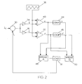
- Figure 2 shows the general arrangement of a servo-amplifier feedback loop, as modified to incorporate the present invention.
- Command current signal I c is combined with current signal i L from load 32, in summing circuit 30.
- the combined current signal is passed through amplifiers 34 and 36, amplifier 36 being an inverting amplifier, as shown.
- the signals from amplifiers 34 and 36 are fed to comparators 40 and 41, respectively, where they are compared with a dither signal, having a sawtooth or triangular shape, produced by sawtooth wave generator 38.
- the negative of the current signal (-I), taken from amplifier 36, is compared with the dither signal, in comparator 42.
- the dither signal is connected to the inverting input of comparator 42. The connection is such that when the dither signal is less than the negative current signal (-I), the output of the comparator becomes high.
- the output of comparator 42 is the pulse train shown in Figure 1 c. This pulse train is called signal x'.
- the Figures 1 b and 1 c are drawn to the same voltage scale. It should be noted that signals x and x' are independent signals, and are not necessarily mirror images of each other. The latter statement is true because the command current signal, in general, varies with time.
- the signals x and x' are passed through complementing circuits 44 and 46, to generate signals y and y, respectively.
- the latter signals are illustrated in Figures 1 and 1 e, respectively. These signals are strictly dependent on signals x and x', because they are obtained only by complementation.
- FIG. 3 shows the bridge circuits represented in block form in Figure 2.
- the bridge circuits are connected across one power supply, having a voltage of V. Note that, in general, V and V need not be equal; normally, V, the voltage ultimately applied across the load, is much greater than v, the amplitude of the control pulses.
- Bridge A includes switches 60, 62, 64, and 66. These switches are preferably electronic switches, such as transistors.
- Bridge B includes switches 68, 70, 72, and 74, preferably similar to the switches of bridge A.
- Load 32 is connected to the two bridge circuits, through inductors 76, 78, 80, and 82.
- the load may be a motor, or any other inductive or resistive load.
- each of the switches of bridge A is controlled by one of the signals x or y.
- Each of the switches of bridge B is controlled by one of the signals x' or y.
- bridge B places a negative voltage (-V) across the load, because it connects the power supply to the load in the opposite direction from bridge A.
- -V negative voltage
- the effect of bridge B is shown in Figure 1g.
- the net effect of the two bridges is shown in Figure 1h.
- the load "sees" zero volts in Case 2.
- the dither signal is negative, and has an absolute value greater than that of the command signal.
- Signal x is low and signal x' is high.
- signal y is high and signal y is low.
- the only closed switches are now switches 60, 66, 68, and 74.
- the circuit path through bridge A includes switch 60, inductor 80, load 32, inductor 76, and switch 66.
- the load therefore "sees” a voltage of -V due to bridge A, as shown in Figure 1f.
- the circuit path through bridge B includes switch 68, inductor 78, load 32, inductor 82, and switch 74.
- the load therefore sees a voltage of + V due to bridge B, as shown in Figure 1g.
- the net effect of the two bridges is that the load "sees" zero volts, as shown in Figure 1 h.
- the inductors are necessary to prevent short circuits in Cases 2 and 4.
- Case 2 for example, without the inductors, there would be a direct path from the power supply (+ V), through switch 64, switch 70, and back to the power supply. There would also be a short circuit through switches 72 and 62.
- Case 4 without the inductors there would be a short circuit from the power supply (+V) through switch 60, through switch 74, and back to the power supply.
- switches 68 and 66 As long as the frequency of pulses is sufficiently high that the period of the pulses is less than the time constant of the inductors, the inductors will prevent short circuits.
- the frequency of pulses in Figure 1 h is twice the frequency of pulses in signal x.
- Signal x is equivalent to a PWM signal of the prior art.
- the circuit of the present invention doubles the frequency of the resultant PWM signal applied to the load.
- the maximum voltage excursion of the signal in Figure 1 is V, i.e. the magnitude of the supply voltage, not 2 V as is true in the prior art.
- current ripple in the load is reduced by increasing the frequency of the PWM signal, and by reducing the voltage excursion of this signal.
- the present invention achieves a reduction in ripple by a factor of four.
- the effective bandwidth of the PWM circuit of the present invention is much greater than in PWM circuits of the prior art because of the fact that the command signal is effectively being sampled more frequently.
- the present invention avoids the undesirable switching losses that would be incurred by simply increasing the frequency of the dither signal.
- the switches are controlled separately by the signals x, x', y, and y. All of these signals, taken separately, have a frequency which is one-half that of the waveform of Figure 1 h. Thus, the switches are not driven at excessive switching rates. But it is the high-frequency waveform of Figure 1 which is "seen" by the load.
- inductors 76 and 78 are magnetically coupled, but wound in an opposed sense. The same is true for the pair of inductors 80 and 82, although the inductors of one pair are not magnetically coupled to the inductors of the other pair.
- the magnetic coupling of the pairs of inductors may be most easily accomplished by winding both inductors of a pair on the same core.
- the electrical connections are otherwise the same as shown in Figure 3. This arrangement gives the system a greater usable bandwidth because, when the bridges are delivering power, the inductive effects tend to cancel. For a given amplifier gain and supply voltage, the bandwidth is limited only by the load itself.
- the invention can be practiced without winding the inductors as stated above, but with reduced bandwidth.
- FIG. 4 is a schematic diagram showing the use of the present invention in driving a three-phase brushless motor.
- the three windings of the brushless motor are designated by reference numerals 61, 62, and 63.
- Each winding is connected to a bridge circuit, designated generally by reference numerals 71, 72, and 73, respectively.
- Each of the bridge circuits is similar to that shown in Figure 3, except that there are only four switches and two inductors in each bridge. It turns out that, because the windings are all connected at one point, each pair of bridges in Figure 4 is electrically equivalent to the full bridge of Figure 3.
- the dotted line 75 illustrates symbolically that the motor shaft (not shown) is connected to an encoder 76.
- the output of the encoder is connected to a suitable logic circuit which controls a current command circuit 78.
- Circuit 78 accepts, as input, the command current, and generates three command currents as outputs. These command currents comprise the command "subsignals" for each bridge.
- the command currents are used to generate three separate trains of pulses, in the manner described in connection with Figures 1 and 2, and the pulses are used to control the bridges in a similar manner.
- the pulses are generated, and applied to the switches of each bridge, substantially simultaneously.
- FIG 3 there is one pair of bridges connected across the load.
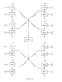
- Figure 5 illustrates an alternative embodiment wherein there are two such pairs of bridges. As can be seen from the drawings, this embodiment is different from that of Figure 4.
- each switch is designated by a rectangle which has a three-character label of the general form "nXm", where n and m are integers, and X represents either the letter “A” or the letter “B".
- the letters "A” and “B” designate switches corresponding to bridges A and B of Figure 3. That is, the letters “A” and “B” indicate switches located on one side of the load or the other, in the sense of Figure 3.
- the integer n is the number of a given switch, within “Set A” or “Set B”.
- the integer m is called the "section” number; a single “section” constitutes a pair of bridges, of the type shown in Figure 3.
- X1 and x 2 represent the same command signal, except that X1 and x 2 are shifted in time by t/4, relative to each other, where t is the period of either pulse train. All of the signals obtained from X1 (i.e. x 1 , x 1 ', and x 1 ') are similarly related, respectively, to the corresponding signals obtained from x 2 .
- x 2 is generated from a triangular waveform (i.e. a dither signal) that has been time-shifted relative to the dither signal used to generate x 1 .
- a dither signal i.e. a triangular waveform
- the first method is preferable because the same signal is, in effect, being sampled twice as often as would be done in the second method, thus increasing the effective bandwidth of the system.
- the inductors are preferably connected in the same sense as described with respect to the embodiment of Figure 3. This means of connection is indicated by the dots, as before. However, note that in Figure 5, while pairs of inductors within one section are coupled, the inductors belonging to different sections are not coupled.
- Figure 5 generates less ripple than does the circuit of Figure 3.
- Figure 5 shows two pairs of bridges connected across the load in parallel. The pairs of bridges may interact slightly with each other, but the voltage fluctuations at the nodes are low, and the interactions have been found not to affect adversely the performance of the circuit.
- the command signal can be used to generate three time-shifted pulse trains x 1 , x 2 , and x 3 .
- Each pulse train is shifted by t/6, where t is the period of the pulse trains.
- t is the period of the pulse trains.
- the signals x can again be generated according to one of at least two methods.
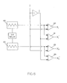
- Figure 8 illustrates the preferred method.
- N equals 2, but the concept is the same for any value of N.
- command signal I is compared with dither signals 120 and 122, in comparators 130 and 132, to yield signals X1 and x 2 , respectively.
- the inverted command signal is compared with dither signals 120 and 122, in comparators 131 and 133, to yield signals x 1 ' and X2 ', respectively.
- Dither signal 122 comprises the same triangular wave as dither signal 120, except that it has been shifted in time by t/4, where t is the period of the dither signals.
- the circuit of Figure 8 therefore produces pulse train signals x 1 , x 2 , x 1 ', and X2 ', which are used in circuits similar to those of Figures 5 and 6.
- the method illustrated in Figure 8 can be generalized to include the case of N time-shifted dither signals.
- the time-shift between successive dither signals is t/2N, where t is the period of the dither signals.
- the signals x ; ' can be generated in several equivalent ways.
- the ith "primed" signal x ; ' can be obtained by comparing the command signal with a time-shifted version of the ith dither signal (the time-shift being t/2, where t is the period of the dither signal), or by comparing the command signal with the inverse of the ith dither signal.
- the latter methods are equivalent to each other, and are also equivalent to the method of comparing the ith dither signal with the inverted command signal, which is the method shown in Figure 8. The latter procedure is believed to be the simplest.
- the second method of generating the signals x is as follows.
- the signal X1 is generated by a circuit similar to that of Figure 2, and is then applied, in parallel, to N-1 separate time-shifting networks, to produce the desired number of time-shifted signals x.
- this method is preferably done by computer, using a numerical algorithm for performing the time-shifting.
- the first method is generally preferred, because the use of N time-shifted dither signals means that the command signal is sampled N times as often as in the second method, and thus the bandwidth of the circuit is increased.
- FIG. 7 is a schematic diagram showing the use of the present invention in a magnetic resonance imaging (MRI) system.
- MRI systems are commonly used for medical diagnosis, and require high-power driver amplifiers for the gradient coils which are critical to the MRI process.
- the MRI system includes a large permanent magnet 100 and gradient coils 102 which surround patient 104.
- the drawing shows only one gradient coil, it is understood that item 102 can symbolically represent a plurality of separate coils.
- the gradient coils modify the magnetic field due to the permanent magnet, i.e. they produce a gradient in the magnetic field, and thereby allow the apparatus to excite atoms in selected portions of the patient's body. Changing the current in the gradient coils therefore permits the apparatus to scan various parts of the patient's body, without using any moving mechanical parts.
- the gradient coils 102 of Figure 7 are driven by driver 106.
- Driver 106 represents any of the above-described PWM circuits; the coils 102 represent the "load" for the PWM circuits. Because the ripple current in the coils is very low, due to the features discussed earlier, it is possible to achieve very precise scanning of various parts of the body.
- element 106 can represent a plurality of separate drivers. For example, there can be one driver for each gradient coil.
- the invention can also be used with a switching power supply. That is, the bridge circuit of the present invention could be used to drive a transformer instead of a motor, and the control voltage could be fixed or variable.
- the present invention can be modified in various other ways.
- the electronic switches can be replaced with equivalent devices.
- the invention need not be limited to the particular bridge topologies described herein, but may include other ways of implementing the method represented in Figure 1.
- the PWM circuit be capable of determining whether the absolute value of the dither signal is greater or less than that of the command signal.
- the output of a circuit which determines these conditions could be used to produce a voltage across the load.
- a first voltage would be applied across the load when the absolute value of the dither signal is greater than that of the command signal; a second voltage, having a different value, would be applied when the absolute value of the dither signal is less than that of the command signal.
- the first voltage is V
- the second voltage is zero.
Landscapes
- Engineering & Computer Science (AREA)
- Power Engineering (AREA)
- Inverter Devices (AREA)
- Arrangements For Transmission Of Measured Signals (AREA)
- Magnetic Resonance Imaging Apparatus (AREA)
Applications Claiming Priority (2)
| Application Number | Priority Date | Filing Date | Title |
|---|---|---|---|
| US563715 | 1990-08-07 | ||
| US07/563,715 US5081409A (en) | 1989-11-13 | 1990-08-07 | Pulse-width modulated circuit for driving a load |
Publications (2)
| Publication Number | Publication Date |
|---|---|
| EP0470499A2 true EP0470499A2 (de) | 1992-02-12 |
| EP0470499A3 EP0470499A3 (en) | 1992-05-06 |
Family
ID=24251602
Family Applications (1)
| Application Number | Title | Priority Date | Filing Date |
|---|---|---|---|
| EP19910112898 Withdrawn EP0470499A3 (en) | 1990-08-07 | 1991-07-31 | Pulse-width modulated circuit for driving a load |
Country Status (3)
| Country | Link |
|---|---|
| US (1) | US5081409A (de) |
| EP (1) | EP0470499A3 (de) |
| JP (1) | JPH0660286A (de) |
Cited By (1)
| Publication number | Priority date | Publication date | Assignee | Title |
|---|---|---|---|---|
| EP0618678A3 (de) * | 1993-04-01 | 1995-08-16 | Ford Motor Co | Digitaler Pulsbreitenmodulator unter Verwendung eines proportionalen Zittersignals. |
Families Citing this family (21)
| Publication number | Priority date | Publication date | Assignee | Title |
|---|---|---|---|---|
| US5399908A (en) * | 1992-06-26 | 1995-03-21 | Kollmorgen Corporation | Apparatus and method for forced sharing of parallel MOSFET switching losses |
| US5493487A (en) * | 1993-02-09 | 1996-02-20 | Performance Controls, Inc. | Electronic switching circuit |
| US5379209A (en) * | 1993-02-09 | 1995-01-03 | Performance Controls, Inc. | Electronic switching circuit |
| US5365422A (en) * | 1993-06-01 | 1994-11-15 | Performance Controls, Inc. | Pulse-width modulated circuit for applying current to a load |
| US5345160A (en) * | 1993-06-02 | 1994-09-06 | Henri Corniere | Variable frequency control system for single phase induction motors |
| US5497062A (en) * | 1993-09-20 | 1996-03-05 | Performance Controls, Inc. | Digital pulse-width modulated system for providing current to a load |
| US5638260A (en) * | 1995-05-19 | 1997-06-10 | Electronic Measurements, Inc. | Parallel resonant capacitor charging power supply operating above the resonant frequency |
| US5629616A (en) * | 1995-07-13 | 1997-05-13 | Performance Conrols, Inc. | Circuit for measuring current in class-d amplifiers |
| US5646837A (en) * | 1995-12-19 | 1997-07-08 | Performance Controls, Inc. | Pulse-width modulated circuit with improved linearity |
| US5903449A (en) * | 1998-06-09 | 1999-05-11 | General Electric Company | Bi-directional power control system for voltage converter |
| JP2003524765A (ja) | 1998-11-30 | 2003-08-19 | エムティエス・システムズ・コーポレーション | パルス幅変調された増幅器における電流を測定するための改善された動的応答を持つ回路 |
| US6353354B1 (en) | 1999-09-28 | 2002-03-05 | Mts Systems Corporation | Pulse-width modulated bridge circuit within a second bridge circuit |
| US6534967B1 (en) | 2000-09-25 | 2003-03-18 | Mts Systems Corporation | Dual totem current sensor for measuring load current in an H-bridge power stage |
| WO2002049197A2 (de) * | 2000-12-14 | 2002-06-20 | Otto Junker Gmbh | Verfahren zur speisung einer induktiven last mit parallelgeschalteten weichschaltenden wechselrichtern |
| JP3890906B2 (ja) * | 2001-03-09 | 2007-03-07 | 松下電器産業株式会社 | ブラシレスモータの駆動装置およびそれを使用するモータ |
| MY144264A (en) * | 2001-11-29 | 2011-08-29 | Transform Solar Pty Ltd | Semiconductur texturing process |
| US6930483B2 (en) * | 2003-08-01 | 2005-08-16 | General Electric Company | Method/system for switched frequency ripple reduction in MRI gradient coils |
| ATE444588T1 (de) * | 2004-02-03 | 2009-10-15 | Ebm Papst St Georgen Gmbh & Co | Elektronisch kommutierter motor und verfahren zur steuerung eines solchen |
| US7531975B1 (en) | 2004-10-13 | 2009-05-12 | Marvell International Ltd. | Adjustable frequency PWM driver |
| DE102012222944A1 (de) * | 2012-12-12 | 2014-06-12 | Robert Bosch Gmbh | Parallelschaltung mehrerer Halbbrücken in H-Brücken-Schaltungsbausteinen |
| EP2747270B1 (de) | 2012-12-21 | 2014-10-15 | Inmotion Technologies AB | Brückenzweig |
Family Cites Families (24)
| Publication number | Priority date | Publication date | Assignee | Title |
|---|---|---|---|---|
| KR900000643B1 (ko) * | 1959-03-26 | 1990-02-02 | 산요덴끼 가부시기가이샤 | 인버어터 장치 |
| US3260912A (en) * | 1963-06-19 | 1966-07-12 | Gen Motors Corp | Power amplifier employing pulse duration modulation |
| US3393363A (en) * | 1963-10-07 | 1968-07-16 | Forster Ind Inc | Amplifying means employing pulse width modulation |
| US3351873A (en) * | 1964-07-08 | 1967-11-07 | Hitachi Ltd | Analog to digital converter employing noise rejection signal modulator |
| US3535657A (en) * | 1967-09-13 | 1970-10-20 | Webb James E | Pulse-width modulation multiplier |
| US3849709A (en) * | 1973-04-25 | 1974-11-19 | Beeman H | Motor control system |
| US3883786A (en) * | 1973-10-12 | 1975-05-13 | Gen Electric | Pulse width modulated servo system |
| FR2266978B1 (de) * | 1974-04-05 | 1976-12-10 | Ragonot Ets | |
| AT343226B (de) * | 1974-12-30 | 1978-05-10 | Elin Union Ag | Schaltungsanordnung fur vorzugsweise der lichtbogenschweissung dienende gleichstromsteller |
| US4388579A (en) * | 1981-07-17 | 1983-06-14 | The United States Of America As Represented By The United States Department Of Energy | Control system for a wound-rotor motor |
| EP0077075B1 (de) * | 1981-10-14 | 1986-07-16 | Hitachi, Ltd. | Digitales Abspielgerät zum Reproduzieren einer digitalen Signalfolge |
| GB2140987B (en) * | 1983-04-15 | 1986-11-19 | Hitachi Ltd | Control apparatus for current type inverter |
| JPH07108095B2 (ja) * | 1984-01-20 | 1995-11-15 | 株式会社日立製作所 | インバータ装置及びその制御方法 |
| EP0157202B1 (de) * | 1984-03-08 | 1989-10-04 | Kabushiki Kaisha Meidensha | Pulsgenerator mit digitaler Pulsweitenmodulation |
| US4584505A (en) * | 1984-06-14 | 1986-04-22 | Yeongchoon Chung | Torque-speed control system for asynchronous D.C. brushless motor |
| US4686436A (en) * | 1984-07-06 | 1987-08-11 | General Electric Company | Electronic control circuit, electronically commutated motor system and method for controlling same, laundry apparatus, and methods for operating apparatus for switching high voltage DC and for controlling electrical load powering apparatus |
| DE3433886A1 (de) * | 1984-09-14 | 1986-03-27 | Siemens AG, 1000 Berlin und 8000 München | Steuereinrichtung fuer einen gleichstrom-halbleitersteller |
| US4706180A (en) * | 1985-11-29 | 1987-11-10 | York International Corporation | Pulse width modulated inverter system for driving single phase a-c induction motor |
| US4626803A (en) * | 1985-12-30 | 1986-12-02 | General Electric Company | Apparatus for providing a carrier signal with two digital data streams I-Q modulated thereon |
| GB8611663D0 (en) * | 1986-05-13 | 1986-06-18 | Oxford Magnet Tech | Frequency multiplying circuit |
| US4689802A (en) * | 1986-05-22 | 1987-08-25 | Chrysler Motors Corporation | Digital pulse width modulator |
| DE3619353A1 (de) * | 1986-06-09 | 1987-12-10 | Philips Patentverwaltung | Pulsbreitenmodulator |
| US4763059A (en) * | 1987-06-23 | 1988-08-09 | General Electric Company | Method and apparatus for induction motor drive |
| US4904919A (en) * | 1988-06-21 | 1990-02-27 | Allen-Bradley Company, Inc. | Dual mode control of a PWM motor drive for current limiting |
-
1990
- 1990-08-07 US US07/563,715 patent/US5081409A/en not_active Expired - Lifetime
-
1991
- 1991-07-16 JP JP3175428A patent/JPH0660286A/ja active Pending
- 1991-07-31 EP EP19910112898 patent/EP0470499A3/en not_active Withdrawn
Cited By (1)
| Publication number | Priority date | Publication date | Assignee | Title |
|---|---|---|---|---|
| EP0618678A3 (de) * | 1993-04-01 | 1995-08-16 | Ford Motor Co | Digitaler Pulsbreitenmodulator unter Verwendung eines proportionalen Zittersignals. |
Also Published As
| Publication number | Publication date |
|---|---|
| EP0470499A3 (en) | 1992-05-06 |
| US5081409A (en) | 1992-01-14 |
| JPH0660286A (ja) | 1994-03-04 |
Similar Documents
| Publication | Publication Date | Title |
|---|---|---|
| US5081409A (en) | Pulse-width modulated circuit for driving a load | |
| US5070292A (en) | Pulse-width modulated circuit for driving a load | |
| CN102484433B (zh) | 用于向负载供应电力的电源、方法和计算机程序产品 | |
| EP0987818B1 (de) | Schaltverstärker zum Generieren von kontinuierlichen, willkürlichen Funktionen für Spülen bei der Magnetresonanz-Bildgebung | |
| US5140510A (en) | Constant frequency power converter | |
| US5519601A (en) | Pulse-width modulated circuit for applying current to a load | |
| US5663647A (en) | Switching gradient amplifier with adjustable DC bus voltage | |
| JP3831020B2 (ja) | ブリッジ回路の駆動方法、ブリッジ回路の駆動回路及びディスク・ドライブ | |
| US6348775B1 (en) | Drive wave form synchronization for induction motors | |
| US6353354B1 (en) | Pulse-width modulated bridge circuit within a second bridge circuit | |
| US5216345A (en) | Mixed mode stepper motor controller and method | |
| JP5555627B2 (ja) | 電流を生成するための方法および構造 | |
| JPH0618565B2 (ja) | 変成器結合勾配高速化回路 | |
| KR102603514B1 (ko) | 전력 컨버터 및 전력 컨버터를 포함하는 mri시스템 | |
| JP2004266884A (ja) | スイッチング電源式電源装置およびそれを用いた核磁気共鳴イメージング装置 | |
| JP2006516439A (ja) | 複数の出力レベルを有する精密な傾斜増幅器 | |
| CN100497980C (zh) | 具有简化布线的磁轴承装置 | |
| US5105153A (en) | Gradient speed-up circuit for nmr system | |
| JPH03155833A (ja) | 高速nmr映像化装置用勾配電流高速化回路 | |
| WO2016040596A1 (en) | Switching amplifier with zero voltage switching and balanced thermal control algorithm | |
| US6856107B2 (en) | Linear-motion engine controller and related method | |
| US6031422A (en) | Power amplifier and nuclear magnetic resonance tomography apparatus employing same | |
| Ates et al. | Sliding mode control of a switched reluctance motor drive with four-switch Bi-Directional DC-DC converter for torque ripple minimization | |
| NL2022622B1 (en) | Electric power converter with inductively coupled parallel power stacks | |
| US5260645A (en) | Power supplies |
Legal Events
| Date | Code | Title | Description |
|---|---|---|---|
| PUAI | Public reference made under article 153(3) epc to a published international application that has entered the european phase |
Free format text: ORIGINAL CODE: 0009012 |
|
| AK | Designated contracting states |
Kind code of ref document: A2 Designated state(s): AT BE CH DE DK ES FR GB GR IT LI LU NL SE |
|
| PUAL | Search report despatched |
Free format text: ORIGINAL CODE: 0009013 |
|
| AK | Designated contracting states |
Kind code of ref document: A3 Designated state(s): AT BE CH DE DK ES FR GB GR IT LI LU NL SE |
|
| STAA | Information on the status of an ep patent application or granted ep patent |
Free format text: STATUS: THE APPLICATION IS DEEMED TO BE WITHDRAWN |
|
| 18D | Application deemed to be withdrawn |
Effective date: 19921107 |