EP0470784A2 - Verfahren zum selektiven Auftragen einer Dünnschicht - Google Patents
Verfahren zum selektiven Auftragen einer Dünnschicht Download PDFInfo
- Publication number
- EP0470784A2 EP0470784A2 EP91307148A EP91307148A EP0470784A2 EP 0470784 A2 EP0470784 A2 EP 0470784A2 EP 91307148 A EP91307148 A EP 91307148A EP 91307148 A EP91307148 A EP 91307148A EP 0470784 A2 EP0470784 A2 EP 0470784A2
- Authority
- EP
- European Patent Office
- Prior art keywords
- wafer
- chemical vapor
- vapor deposition
- reactor
- semiconductor wafer
- Prior art date
- Legal status (The legal status is an assumption and is not a legal conclusion. Google has not performed a legal analysis and makes no representation as to the accuracy of the status listed.)
- Withdrawn
Links
Images

Classifications
-
- C—CHEMISTRY; METALLURGY
- C23—COATING METALLIC MATERIAL; COATING MATERIAL WITH METALLIC MATERIAL; CHEMICAL SURFACE TREATMENT; DIFFUSION TREATMENT OF METALLIC MATERIAL; COATING BY VACUUM EVAPORATION, BY SPUTTERING, BY ION IMPLANTATION OR BY CHEMICAL VAPOUR DEPOSITION, IN GENERAL; INHIBITING CORROSION OF METALLIC MATERIAL OR INCRUSTATION IN GENERAL
- C23C—COATING METALLIC MATERIAL; COATING MATERIAL WITH METALLIC MATERIAL; SURFACE TREATMENT OF METALLIC MATERIAL BY DIFFUSION INTO THE SURFACE, BY CHEMICAL CONVERSION OR SUBSTITUTION; COATING BY VACUUM EVAPORATION, BY SPUTTERING, BY ION IMPLANTATION OR BY CHEMICAL VAPOUR DEPOSITION, IN GENERAL
- C23C16/00—Chemical coating by decomposition of gaseous compounds, without leaving reaction products of surface material in the coating, i.e. chemical vapour deposition [CVD] processes
- C23C16/44—Chemical coating by decomposition of gaseous compounds, without leaving reaction products of surface material in the coating, i.e. chemical vapour deposition [CVD] processes characterised by the method of coating
- C23C16/48—Chemical coating by decomposition of gaseous compounds, without leaving reaction products of surface material in the coating, i.e. chemical vapour deposition [CVD] processes characterised by the method of coating by irradiation, e.g. photolysis, radiolysis, particle radiation
- C23C16/482—Chemical coating by decomposition of gaseous compounds, without leaving reaction products of surface material in the coating, i.e. chemical vapour deposition [CVD] processes characterised by the method of coating by irradiation, e.g. photolysis, radiolysis, particle radiation using incoherent light, UV to IR, e.g. lamps
-
- C—CHEMISTRY; METALLURGY
- C23—COATING METALLIC MATERIAL; COATING MATERIAL WITH METALLIC MATERIAL; CHEMICAL SURFACE TREATMENT; DIFFUSION TREATMENT OF METALLIC MATERIAL; COATING BY VACUUM EVAPORATION, BY SPUTTERING, BY ION IMPLANTATION OR BY CHEMICAL VAPOUR DEPOSITION, IN GENERAL; INHIBITING CORROSION OF METALLIC MATERIAL OR INCRUSTATION IN GENERAL
- C23C—COATING METALLIC MATERIAL; COATING MATERIAL WITH METALLIC MATERIAL; SURFACE TREATMENT OF METALLIC MATERIAL BY DIFFUSION INTO THE SURFACE, BY CHEMICAL CONVERSION OR SUBSTITUTION; COATING BY VACUUM EVAPORATION, BY SPUTTERING, BY ION IMPLANTATION OR BY CHEMICAL VAPOUR DEPOSITION, IN GENERAL
- C23C16/00—Chemical coating by decomposition of gaseous compounds, without leaving reaction products of surface material in the coating, i.e. chemical vapour deposition [CVD] processes
- C23C16/04—Coating on selected surface areas, e.g. using masks
- C23C16/047—Coating on selected surface areas, e.g. using masks using irradiation by energy or particles
Definitions
- This invention relates, in general, to manufacturing semiconductor devices, and more particularly, to the generation of patterned thin films on a semiconductor device.
- Formation of geometric patterns is an integral part of manufacturing semiconductor devices.
- the patterns that are generated define physical components of devices that are to be manufactured.
- the generation of patterns on semiconductor wafer materials is usually divided into three major steps: deposition, photolithography, and etching.
- Deposition is a process in which a film is applied onto a surface.
- Film types that are commonly used in manufacturing of semiconductors range from insulators to conductors. Generally, each kind of film that is deposited requires a different piece of equipment and a wide variety of process conditions.
- Photolithography is a process of defining patterns in a photo sensitive material, know as photoresist, by projecting images that are desired into the body of a photoresist film.
- the photolithography process is a very complicated set of conditions and processes but, can be broken down into three major steps or processes.
- First is an application of photoresist material to the surface of a semiconductor wafer. Generally, this process is achieved by applying a measured amount of liquid photoresist material in the center of a semiconductor wafer. The semiconductor wafer is then spun at high RPM to produce a uniform film of photoresist over the entire wafer surface. The wafer is then heated slightly, which drives off some volatile solvents, gels the film, and prepares it for an image projection step.
- This array of processes and conditions is accomplished by a complicated piece of equipment called a wafer coater.
- Second, is projecting desired images or patterns onto the photoresist coated wafer. Projection of these images can be achieved by a variety of cameras that are commercially available. Generally, these cameras project desired images or patterns by illuminating a reticle image that casts very sharp patterns of light and dark areas. In positive photoresist systems, exposure to light causes chemical reactions to take place in the photoresist, which changes the solubility of the exposed photoresist in an aqueous base. Therefore, areas that are illuminated are exposed and areas that are in darkness are not exposed. Third, is development of images that have been exposed from the projection step.
- Images that have been projected into the photoresist film are made into three dimensional patterns in the photoresist film that has been applied to the wafer. This step is accomplished by taking advantage of the solubility differences between exposed photoresist and non-exposed photoresist.
- Application of an aqueous base to exposed areas of photoresist dissolves the film away whereas, application of the aqueous base to unexposed photoresist does not dissolve the film away.
- Completion of the development process leaves three dimensional patterns of unexposed photoresist on the wafer.
- the patterns formed by the photoresist are now ready for transferring or etching into the underlying deposited film.
- Developing photoresist can be done with a number of different processes and equipment sets.
- Etching is a process of transferring a photoresist pattern to an underlying film. Etching these patterns is accomplished either by chemical or physical methods or a combination of the two. Etching also requires the use of different pieces of equipment in which a wide variety of chemistries is used.
- the invention provides an apparatus and method for selectively depositing a thin film by projecting geometric features on a semiconductor wafer.
- the semiconductor wafer is mounted in a chemical vapor deposition chamber that has a projection means.
- a gas species that is flowing though the chemical vapor deposition chamber has a low photodissociation energy level.
- Directing an ultraviolet light or equivalent energy source though the projection means to generate a predetermined geometric pattern on the semiconductor wafer so that at least a patterned monomolecular film is produced. This monomolecular film can then be used to grow a thicker film, if desired.
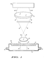
- Ultraviolet light source 10 is shown as a modular block. Ultraviolet light source 10 provides illumination and radiant energy to project an image on wafer 17. Ultraviolet light source 10 can contain a variety of mirrors, lamps, and filters. Generally, though a mirror is positioned so as to be able to reflect radiation from a lamp and direct its radiation though a filter. Lamps are usually Mercury Arc that emit several lines of intense wave lengths in the ultraviolet radiation range. Filtering radiation allows for selection of a specific wave length of light. Dotted lines 16 represent the light path of radiation as it passes though various elements of a projection system.
- Condensing lens system 11 Radiation from ultraviolet light source 10 is directed to condensing lens system 11.
- Condensing lens system 11 can be composed of a multitude of lens depending upon requirements that are optically necessary. Condensing lens system 11 concentrates radiation from ultraviolet light source 10, as well as, ensuring that an even illumination across reticle or mask 12 is accomplished.
- Reticle or mask 12 is where geometric patterns that are desired to be projected are kept.
- Reticle or mask 12 is manufactured by a well known photolithographic process.
- Reticle or mask 12 is generally made of optically clear quartz plates or the like. On one side of reticle or mask 12 there is a pattern depicted in chrome.
- Radiation from condensing lens system 11 shines though the reticle or mask 12 to generate a pattern of light and dark spaces that correspond to a pattern depicted in chrome on reticle or mask 12. This pattern then illuminates reduction lens system 13.
- Reduction lens system 13 can be composed of many different lens elements. Reduction lens system 13 reduces the pattern generated from reticle or mask 12 to desired size. Reduction lens that are most commonly used in manufacturing semiconductor devices are 10X and 5X. Therefore, in the case of a 10X reduction lens a ten micron line on reticle or mask 12 will yield a one micron line after passing though reduction lens system 13. It should be understood that other sources of imaging apparatus could be utilized to project images such as a Perkin Elmer scanning system, a laser direct write system, an Electron Beam "E Beam" direct write system, or the like.
- Window 14 is an interface between the optical system and a chemical vapor deposition system.
- Window 14 is composed of an ultraviolet transparent material such as quartz or the like, so that transmission of patterned radiation though window 14 can be directed to wafer 17 without loss of intensity or resolution.
- Window 14 is part of a chemical vapor deposition reactor or chamber 18 and is connected to chemical vapor deposition reactor 18 in such a manner that either low or high pressure chemistry may be used in reactor 18. The selection of high or low pressure chemistry is dependent upon chemistry of gases that are used. Radiation that passes though window 14 and though chemical vapor deposition reactor 18 ultimately strikes wafer 17 mounted in chemical vapor deposition reactor 18.
- Gas inject port 19 allows for the entrance of a reactive gas into the chamber of chemical vapor deposition reactor 18. It should be understood that more than one gas could be injected into chemical vapor deposition body 18 from gas inject port 19. Once the gas is injected into chemical vapor deposition reactor 18 it can be handled either dynamically or statically. Dynamically, injected gas travels across wafer 17. As gas travels across wafer 17 energy from the projection system is sufficient to cause at least a monomolecular deposition on wafer 17. Deposition is caused by either the localized thermal heating of wafer 17 itself or by gas phase nucleation and proximity deposition. Unused gases are expelled though exhaust port 21. The deposition on wafer 17 which is created by projection of radiation from the projection system is a duplication of the pattern on reticle or mask 12.
- the gas enters chemical vapor deposition reactor 18.
- a predetermined process parameter such as pressure, flow rate, temperature, time, or the like is reached suitable valving closes and holds the gas in chemical vapor deposition reactor 18.
- Energy from projection means is then directed onto wafer 17.
- the energy from the projection means is sufficient to cause deposition of at least a selective monolayer of film on wafer 17. Unused gases are then expelled though exhaust port 21.
- the invention utilizes a type of gas that is customized so that when a radiation source is projected onto the wafer there is sufficient energy to dissociate the gas into at least two parts.
- One part is deposited on the wafer surface in a predetermined pattern and the other is exhausted though port 21.
- the deposited portion of the gas forms the geometric patterns that are required to build geometric features such as metal interconnect lines, dielectric isolation features, semiconductor features, or the like.
- Gases that are suitable for use in this invention are volatile organometallics.
- copper (I) species such as amines, phosphites, arsines, carbonyls, alkyls, diketonates, or the like may be used to practice this invention.
- Radiation sources can be of many different kinds such as ultraviolet, electron beam, Laser, or the like.
- the gas is a low activiation energy photodissociation gas.
- Photodissociation is dissociation caused by a patterned light leam or a direct write system such as an E - beam system, or the like. It is well known that a direct write system does not require a mask or reticle such as illustrated in FIG. 1.
- FIG. 2 pictorially illustrates one embodiment of the present invention in a multi-chamber cluster tool arrangement.
- Cluster tools are highly automated and it should be understood that processes and movement of wafers are controlled by a computer managing system.
- Cluster tools also offer an advantage of being able to keep wafers clean and under vacuum during processing and wafer movement procedures.
- Wafers are introduced to wafer storage chamber 29.
- Wafer storage chamber 29 can be evacuated or not depending upon specific uses.
- Wafer storage chamber 29 also must have room for at least one cassette 28, but can have more than one cassette as is shown in FIG. 2.
- Wafer cassette 28 is a storage device which holds wafers. Generally, cassettes are manufactured so that individual wafers are kept in separate slots with a specified amount of space between them.
- This space is sufficient so that one stored wafer will not rub against another stored wafer and create particles. It also allows sufficient space for easy access by a robot arm 31 so that wafers may be retrieved and returned for processing.
- Wafers are retrieved from cassettes 28 from wafer storage 29 and moved to vacuum wafer storage 33. Movement of wafers from cassette 28 to vacuum wafer storage 29 is accomplished by robot arm 31. Once wafers are in vacuum storage 33 they are then capable of being moved to any one of the available reactors or chambers. Movement from wafer storage 33 to any of the available reactors is accomplished by a robot arm 32. It should be understood that robot arm 31 and robot arm 32 need to be in communication with each other so as to avoid wafer handling problems.
- a typical process moves wafer 34 from vacuum wafer storage 33 to pre-treatment reactor 22.
- Pre-treatment reactor 22 cleans and predisposes wafer 35 for chemical vapor deposition lithographic (CVD-Lith) reactor 23.
- Predisposing wafer 35 results in a treatment of wafer surface 35 in a manner so as to facilitate pattern deposition on wafer 36 in CVD-Lith reactor 23.
- Photodissociation reactions are chemical reactions that occur upon exposure to light that causes separation of a molecule into at least two parts. It should be understood that this reaction is dependent upon wavelength, energy input and specific gases that are used. Further, it should be understood that gases can be tailored to dissociate at specific wavelengths and energy levels.
- Robot arm 32 retrieves wafer 35 from pre-treatment reactor 22 after wafer 35 has been processed and moves wafer 35 to CVD-Lith reactor 23.
- CVD-Lith reactor 23 selectively deposits at least a monomolecular film on wafer 36.
- CVD-Lith reactor 23 is shown in one embodiment in more detail in FIG. 1. It should be understood that this is only one embodiment and others can be used.
- Wafer 36 is now moved into a chemical vapor deposition (CVD) chamber or deposition reactor 24 or deposition reactor 26 for selective deposition onto the monomolecular layer provided by CVD-Lith reactor 23. Once full thickness of selective material is achieved in deposition reactor 24 or deposition chamber 26 wafer 37 or wafer 38 is removed by robot arm 32 and placed in vacuum chamber 33. Completed wafer 34 is then moved back to cassettes 28.
- CVD chemical vapor deposition
- Wafer 37 is then moved to deposition reactor 26 for a deposition of a different film such as nitride, oxide or the like.
- Wafer 38 is then moved to reactor 27 where surface modification of wafer 39 can be done.
- Wafer 39 is then moved back to deposition reactor 26 for further deposition.
- Wafer 38 can then either be moved to reactor 27 for further surface modification sequencing or can be removed from the system though vacuum chamber 33. It should be understood that cluster tools lend themselves to integrated processing, which makes it possible to deposit or etch a wide variety of film types.
- wafer 34 when wafer 34 is in CVD-Lith reactor 23 for CVD-Lith selective deposition, the deposition is made to full thickness. Wafer 36 is then moved on for further processing.
- the geometric features and patterns that are derived can be conductive lines or other portions of semiconductor devices depending upon the gases used during the chemical vapor deposition lithographic step.
- reactors are very modular in nature. This modularity allows for absolute freedom to located reactors in any position around the cluster tool. It will still be further understood that wafers can be processed in and out of various reactors as many times as is desired.
Landscapes
- Chemical & Material Sciences (AREA)
- Health & Medical Sciences (AREA)
- Toxicology (AREA)
- General Chemical & Material Sciences (AREA)
- Chemical Kinetics & Catalysis (AREA)
- Engineering & Computer Science (AREA)
- Materials Engineering (AREA)
- Mechanical Engineering (AREA)
- Metallurgy (AREA)
- Organic Chemistry (AREA)
- Electrodes Of Semiconductors (AREA)
- Internal Circuitry In Semiconductor Integrated Circuit Devices (AREA)
Applications Claiming Priority (2)
| Application Number | Priority Date | Filing Date | Title |
|---|---|---|---|
| US56509690A | 1990-08-10 | 1990-08-10 | |
| US565096 | 1990-08-10 |
Publications (2)
| Publication Number | Publication Date |
|---|---|
| EP0470784A2 true EP0470784A2 (de) | 1992-02-12 |
| EP0470784A3 EP0470784A3 (en) | 1993-03-03 |
Family
ID=24257199
Family Applications (1)
| Application Number | Title | Priority Date | Filing Date |
|---|---|---|---|
| EP19910307148 Withdrawn EP0470784A3 (en) | 1990-08-10 | 1991-08-02 | Method for selectively depositing a thin film |
Country Status (3)
| Country | Link |
|---|---|
| EP (1) | EP0470784A3 (de) |
| JP (1) | JPH04233727A (de) |
| KR (1) | KR920005253A (de) |
Cited By (4)
| Publication number | Priority date | Publication date | Assignee | Title |
|---|---|---|---|---|
| EP0501278A1 (de) * | 1991-02-28 | 1992-09-02 | Texas Instruments Incorporated | Verfahren zur Herstellung einer Markierung |
| US5460693A (en) * | 1994-05-31 | 1995-10-24 | Texas Instruments Incorporated | Dry microlithography process |
| CN116844994A (zh) * | 2022-03-23 | 2023-10-03 | 广东鸿浩半导体设备有限公司 | 一种用于全晶圆沉积的工艺和设备 |
| US12543517B2 (en) | 2023-05-10 | 2026-02-03 | Tokyo Electron Limited | System and method for semiconductor structure |
Family Cites Families (4)
| Publication number | Priority date | Publication date | Assignee | Title |
|---|---|---|---|---|
| US3378401A (en) * | 1964-02-11 | 1968-04-16 | Minnesota Mining & Mfg | Process for the formation of visible images on a substrate |
| WO1983004269A1 (en) * | 1982-06-01 | 1983-12-08 | Massachusetts Institute Of Technology | Maskless growth of patterned films |
| US4701347A (en) * | 1986-04-18 | 1987-10-20 | American Telephone And Telegraph Company, At&T Bell Laboratories | Method for growing patterned metal layers |
| JP3527624B2 (ja) * | 1997-08-29 | 2004-05-17 | リズム時計工業株式会社 | 時計装置 |
-
1991
- 1991-08-02 EP EP19910307148 patent/EP0470784A3/en not_active Withdrawn
- 1991-08-06 JP JP3219355A patent/JPH04233727A/ja active Pending
- 1991-08-07 KR KR1019910013626A patent/KR920005253A/ko not_active Withdrawn
Cited By (6)
| Publication number | Priority date | Publication date | Assignee | Title |
|---|---|---|---|---|
| EP0501278A1 (de) * | 1991-02-28 | 1992-09-02 | Texas Instruments Incorporated | Verfahren zur Herstellung einer Markierung |
| US6432317B1 (en) | 1991-02-28 | 2002-08-13 | Texas Instruments Incorporated | Method to produce masking |
| US5460693A (en) * | 1994-05-31 | 1995-10-24 | Texas Instruments Incorporated | Dry microlithography process |
| US5700628A (en) * | 1994-05-31 | 1997-12-23 | Texas Instruments Incorporated | Dry microlithography process |
| CN116844994A (zh) * | 2022-03-23 | 2023-10-03 | 广东鸿浩半导体设备有限公司 | 一种用于全晶圆沉积的工艺和设备 |
| US12543517B2 (en) | 2023-05-10 | 2026-02-03 | Tokyo Electron Limited | System and method for semiconductor structure |
Also Published As
| Publication number | Publication date |
|---|---|
| JPH04233727A (ja) | 1992-08-21 |
| EP0470784A3 (en) | 1993-03-03 |
| KR920005253A (ko) | 1992-03-28 |
Similar Documents
| Publication | Publication Date | Title |
|---|---|---|
| US5310624A (en) | Integrated circuit micro-fabrication using dry lithographic processes | |
| US4643799A (en) | Method of dry etching | |
| US4612085A (en) | Photochemical patterning | |
| JP2753930B2 (ja) | 液浸式投影露光装置 | |
| JP5833196B2 (ja) | 気体環境中のフォトレジストをレーザ処理する方法 | |
| US5559584A (en) | Exposure apparatus | |
| KR20040047713A (ko) | 리소그래피 장치 및 디바이스 제조방법 | |
| EP0110882A1 (de) | Maskenlose erzeugung gemusterter schichten | |
| EP0077445B1 (de) | Verfahren zur Herstellung einer elektronischen Schaltkreisstruktur | |
| US4897325A (en) | Contact lithographic fabrication of patterns on large optics | |
| US20010055104A1 (en) | Exposure method and apparatus | |
| US20060194155A1 (en) | Resist pattern forming method and semiconductor device manufacturing method | |
| WO2001061409A2 (en) | Apparatus and method of cleaning reticles for use in a lithography tool | |
| KR900001238B1 (ko) | 레지스트막 건조현상 방법 및 장치 | |
| US3853648A (en) | Process for forming a metal oxide pattern | |
| JPH08227851A (ja) | ホトリソグラフィ方法及びそれに使用するホトリソグラフィシステム | |
| US20070263194A1 (en) | Method of exposing a wafer to a light, and reticle, reticle assembly and exposing apparatus for performing the same | |
| JPH04233727A (ja) | 薄膜の選択的被着方法 | |
| US6781674B1 (en) | System and method to increase throughput in a dual substrate stage double exposure lithography system | |
| JP3563936B2 (ja) | 半導体製造用露光装置およびこれを用いた半導体デバイス製造プロセス | |
| WO1989007285A1 (en) | Integrated circuit micro-fabrication using dry lithographic processes | |
| JPH04151668A (ja) | パターン形成方法 | |
| US5548625A (en) | Method for parallel multiple field processing in X-ray lithography | |
| US20020145710A1 (en) | Exposure apparatus and device manufacturing method using the same | |
| EP0359221B1 (de) | Hochdruck-Photolack Siliconisierungsverfahren und Vorrichtung |
Legal Events
| Date | Code | Title | Description |
|---|---|---|---|
| PUAI | Public reference made under article 153(3) epc to a published international application that has entered the european phase |
Free format text: ORIGINAL CODE: 0009012 |
|
| AK | Designated contracting states |
Kind code of ref document: A2 Designated state(s): DE FR GB |
|
| PUAL | Search report despatched |
Free format text: ORIGINAL CODE: 0009013 |
|
| AK | Designated contracting states |
Kind code of ref document: A3 Designated state(s): DE FR GB |
|
| STAA | Information on the status of an ep patent application or granted ep patent |
Free format text: STATUS: THE APPLICATION IS DEEMED TO BE WITHDRAWN |
|
| 18D | Application deemed to be withdrawn |
Effective date: 19930904 |