EP0470897A1 - Integrierte Speicherschaltung mit Redundanz und verbesserter Adressierung in Testbetriebsart - Google Patents
Integrierte Speicherschaltung mit Redundanz und verbesserter Adressierung in Testbetriebsart Download PDFInfo
- Publication number
- EP0470897A1 EP0470897A1 EP91402169A EP91402169A EP0470897A1 EP 0470897 A1 EP0470897 A1 EP 0470897A1 EP 91402169 A EP91402169 A EP 91402169A EP 91402169 A EP91402169 A EP 91402169A EP 0470897 A1 EP0470897 A1 EP 0470897A1
- Authority
- EP
- European Patent Office
- Prior art keywords
- columns
- memory
- address
- column
- defective
- Prior art date
- Legal status (The legal status is an assumption and is not a legal conclusion. Google has not performed a legal analysis and makes no representation as to the accuracy of the status listed.)
- Granted
Links
- 230000015654 memory Effects 0.000 title claims abstract description 63
- 238000012360 testing method Methods 0.000 title claims abstract description 61
- 230000002950 deficient Effects 0.000 claims abstract description 32
- 230000000295 complement effect Effects 0.000 claims description 15
- 230000004044 response Effects 0.000 claims description 2
- 230000004048 modification Effects 0.000 description 5
- 238000012986 modification Methods 0.000 description 5
- IUVCFHHAEHNCFT-INIZCTEOSA-N 2-[(1s)-1-[4-amino-3-(3-fluoro-4-propan-2-yloxyphenyl)pyrazolo[3,4-d]pyrimidin-1-yl]ethyl]-6-fluoro-3-(3-fluorophenyl)chromen-4-one Chemical compound C1=C(F)C(OC(C)C)=CC=C1C(C1=C(N)N=CN=C11)=NN1[C@@H](C)C1=C(C=2C=C(F)C=CC=2)C(=O)C2=CC(F)=CC=C2O1 IUVCFHHAEHNCFT-INIZCTEOSA-N 0.000 description 2
- 230000005540 biological transmission Effects 0.000 description 2
- XUIMIQQOPSSXEZ-UHFFFAOYSA-N Silicon Chemical compound [Si] XUIMIQQOPSSXEZ-UHFFFAOYSA-N 0.000 description 1
- 230000003213 activating effect Effects 0.000 description 1
- 230000000694 effects Effects 0.000 description 1
- 238000004519 manufacturing process Methods 0.000 description 1
- 230000003472 neutralizing effect Effects 0.000 description 1
- 229910052710 silicon Inorganic materials 0.000 description 1
- 239000010703 silicon Substances 0.000 description 1
- 238000006467 substitution reaction Methods 0.000 description 1
- 230000009897 systematic effect Effects 0.000 description 1
- 235000012431 wafers Nutrition 0.000 description 1
Images
Classifications
-
- G—PHYSICS
- G11—INFORMATION STORAGE
- G11C—STATIC STORES
- G11C29/00—Checking stores for correct operation ; Subsequent repair; Testing stores during standby or offline operation
- G11C29/70—Masking faults in memories by using spares or by reconfiguring
- G11C29/78—Masking faults in memories by using spares or by reconfiguring using programmable devices
- G11C29/781—Masking faults in memories by using spares or by reconfiguring using programmable devices combined in a redundant decoder
-
- G—PHYSICS
- G11—INFORMATION STORAGE
- G11C—STATIC STORES
- G11C29/00—Checking stores for correct operation ; Subsequent repair; Testing stores during standby or offline operation
- G11C29/04—Detection or location of defective memory elements, e.g. cell constructio details, timing of test signals
- G11C29/08—Functional testing, e.g. testing during refresh, power-on self testing [POST] or distributed testing
- G11C29/12—Built-in arrangements for testing, e.g. built-in self testing [BIST] or interconnection details
- G11C29/18—Address generation devices; Devices for accessing memories, e.g. details of addressing circuits
- G11C29/24—Accessing extra cells, e.g. dummy cells or redundant cells
Definitions
- the invention relates to memories produced in integrated circuit, very particularly but not exclusively to electrically programmable non-volatile memories.
- the substitution must be transparent, that is to say that he is authorized to send to the addressing address of the memory an address corresponding to a defective column; the internal redundancy circuit then takes care of neutralizing the defective column and of reading or writing information in a cell of a replacement column instead of trying to read or write it in a cell of the defective column .
- This transparency requires placing faulty address recognition circuits, deselection circuits to neutralize defective columns, and routing circuits to replacement columns at the memory input.
- the test consists in particular in programming all the cells from their initial state (blank state) to a "programmed” state and in verifying that they are correctly programmed. It is moreover generally during this test that defective columns are detected and that replacement columns are put into service.
- Testing a memory cell can take a few milliseconds. However, integrated circuits are manufactured in batches, and each batch comprises dozens of silicon wafers each carrying several tens of chips which themselves each carry several tens or hundreds of thousands of memory cells; the testing operations can then take a considerable time since it is necessary to systematically test all the cells.
- the cells be programmed according to a pattern (for example a checkerboard pattern) which allows the simultaneous programming of several columns of memory points.
- a pattern for example a checkerboard pattern
- the test time is divided accordingly.
- a memory is proposed according to the invention in which the addressing means in group test mode, making it possible to address simultaneously a group of several columns, are capable of simultaneously selecting, in order to program them, not only the columns of this group but, if one of the columns in the group is defective and associated with a replacement column, the replacement column.
- a column address decoder receiving on address inputs the bits of a column address and on complementary inputs the complements of these bits, a redundancy memory for storing addresses of defective columns, a circuit for comparing the addresses received and addresses of defective columns;
- the circuit for comparing addresses received and defective addresses comprises a NOR gate with several inputs, each input receiving a bit whose logic level depends on the identity between a bit received on an input of the decoder and a corresponding bit of the redundancy memory ;
- means are provided for selecting a replacement column and simultaneously deselecting a defective column when the output from the NOR gate indicates that a received address is identical to a defective address;
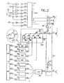
- the group test is controlled by a logic circuit which, in response to a group test control signal, places an identical logic level on at least one input and a corresponding complementary input of the decoder; and the group test command signal is applied to the comparison circuit to prevent the replacement column from being systematically taken out of service during the group test.
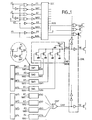
- FIG. 1 the overall architecture of the integrated circuit memory is shown, not allowing a group test after the redundancy has been put into service.
- the example shown is that of a memory with column addressing by four address bits, with two redundancy columns capable of replacing two defective columns, and with a grouped test mode allowing programming of four columns at a time.
- this embodiment is given only by way of a simplified example, the numbers of address bits and of columns being much higher in practice.
- the memory map itself with its rows and columns of cells is not shown; access to the memory cell columns of the memory plane is established by a column address decoder (DEC) whose PYM outputs are equal in number to the number of memory columns: each output line makes it possible to select, when 'it is at the appropriate logical level, a particular column of memory.
- DEC column address decoder
- the decoder receives on address bit inputs and on complementary inputs respectively the address bits A1, A2, A3, A4 and the complements NA1, NA2, NA3, NA4 of these bits.
- a given column is selected by the decoder. But if an input and the corresponding complementary input (for example A1 and NA1) of the decoder are forced to the same logic level 1 (instead of complementary levels 1 and 0), two columns are selected. And if you force two inputs and the two corresponding complementary inputs (for example A1 and A2 and NA1 and NA2) all at the same logic level 1, then four columns are selected simultaneously. The four columns which are thus selected simultaneously are defined by the other address bits (A3 and A4 here).
- a group test control signal G is applied to a set of logic gates (NOR gates) interposed between the address inputs of the memory and the inputs of the decoder.
- G logic level 1
- NOR gates logic gates
- a DSL deselection circuit makes it possible to deselect the column designated by the decoder and to select a replacement column instead.
- This DSL circuit receives the PYM outputs from the decoder and a CAB deselection control signal. If CAB is at logic level 1, the PYM output is inhibited and no longer allows the column designated by the decoder to be selected.
- the signal CAB is supplied by a comparison circuit CMP; it is 1 when the address presented at the input of the decoder is a defective column address.
- the DSL circuit receives the outputs PYM for designating the column to be selected and it supplies, under the control of the deselection signal CAB, as many outputs YM which are command lines for selecting columns from the memory and an additional output YR which is a command line for selecting a first redundant column.
- two redundancy columns are in fact provided, for example one associated with one half of the columns and the other with the other half, or both associated with all of the columns;
- the CAB signal makes it possible to deselect a defective column in order to select the first replacement column instead; this selection is made using the YR command line;
- a CAB signal ' makes it possible to deselect a defective column to select another replacement column by activating another command line YR'.
- the addresses of defective columns, identified during the memory test, are stored in redundancy memories, produced in the form of fuse banks or electrically programmable and non-erasable memories (UPROM).
- a first four-bit address is stored in a memory area MR associated with the first replacement column; another address can be stored in a second redundancy memory zone MR ′ associated with the second replacement column. These two addresses represent the addresses of two defective memory columns.
- the comparison is carried out from circuits organized in the following manner: the faulty column address bits, represented by the outputs NF1, NF2, NF3, NF4, of the memory MR, are used to each command a respective switch SW1, SW2 , SW3, SW4. Each switch also receives the signals present on an input and a respective complementary input of the decoder.
- the switch SW1 receives as control signal NF1 (first defective column address bit) and as signals to switch A1 (first input of the decoder DEC) and NA1 (first complementary input of the decoder).
- NF1 first defective column address bit
- NA1 first complementary input of the decoder
- the output signal XA1 of the switch SW1 is then equal to 0 if the stored address bit corresponds to the address bit received at the input of the memory.
- all the output signals XA1 to XA4 of the switches connected at the output of the redundancy memory all pass to 0.
- the signal of CAB deselection is then activated.
- a simple NOR gate (designated by CMP in the figure) receiving all the signals XA1 to XA4 provides at its output the signal CAB. This gate NOR is here produced by transistors in parallel whose gates receive the signals XA1 to XA4.
- the NOR CMP gate is modified as follows: it receives the complement NG of the signal G of the group test command. This signal NG prohibits the zeroing of the signal CAB under the effect of the signals XA1 and XA2, that is to say the output signals of the switches SW1 and SW2 which correspond to the address bits grouped during the group test.
- bits A3 and A4 correspond to a defective column address
- the signal CAB will go to 1 and allow the selection of the redundant column; indeed, the defective column is then one of the four columns selected by the group test and it must be replaced by the redundant column.
- the four grouped columns should not be deselected since they must be tested (whereas changing the CAB signal to 1 deselects them all); this is why there is interposed in the DSL deselection circuit a logic gate ND receiving the signal CAB or its complement and the signal G of grouped test or its complement; this door neutralizes the deselection when the signal G indicates that we are in group test mode.
- the ND gate prevents the CAB signal from affecting the transmission of the PYM output signals from the decoder to the columns of the memory plane.
Landscapes
- For Increasing The Reliability Of Semiconductor Memories (AREA)
- Techniques For Improving Reliability Of Storages (AREA)
Applications Claiming Priority (2)
| Application Number | Priority Date | Filing Date | Title |
|---|---|---|---|
| FR9010247 | 1990-08-10 | ||
| FR9010247A FR2665793B1 (fr) | 1990-08-10 | 1990-08-10 | Circuit integre de memoire avec redondance et adressage ameliore en mode de test. |
Publications (2)
| Publication Number | Publication Date |
|---|---|
| EP0470897A1 true EP0470897A1 (de) | 1992-02-12 |
| EP0470897B1 EP0470897B1 (de) | 1993-12-15 |
Family
ID=9399605
Family Applications (1)
| Application Number | Title | Priority Date | Filing Date |
|---|---|---|---|
| EP91402169A Expired - Lifetime EP0470897B1 (de) | 1990-08-10 | 1991-08-02 | Integrierte Speicherschaltung mit Redundanz und verbesserter Adressierung in Testbetriebsart |
Country Status (4)
| Country | Link |
|---|---|
| US (1) | US5247481A (de) |
| EP (1) | EP0470897B1 (de) |
| DE (1) | DE69100796T2 (de) |
| FR (1) | FR2665793B1 (de) |
Families Citing this family (11)
| Publication number | Priority date | Publication date | Assignee | Title |
|---|---|---|---|---|
| US5588115A (en) * | 1993-01-29 | 1996-12-24 | Teradyne, Inc. | Redundancy analyzer for automatic memory tester |
| US6101618A (en) * | 1993-12-22 | 2000-08-08 | Stmicroelectronics, Inc. | Method and device for acquiring redundancy information from a packaged memory chip |
| US5530674A (en) * | 1994-04-29 | 1996-06-25 | Sgs-Thomson Microelectronics, Inc. | Structure capable of simultaneously testing redundant and non-redundant memory elements during stress testing of an integrated circuit memory device |
| JP3865828B2 (ja) | 1995-11-28 | 2007-01-10 | 株式会社ルネサステクノロジ | 半導体記憶装置 |
| US5754556A (en) * | 1996-07-18 | 1998-05-19 | Teradyne, Inc. | Semiconductor memory tester with hardware accelerators |
| JPH1166882A (ja) * | 1997-08-19 | 1999-03-09 | Nec Corp | 半導体記憶装置 |
| US6022788A (en) * | 1997-12-23 | 2000-02-08 | Stmicroelectronics, Inc. | Method of forming an integrated circuit having spacer after shallow trench fill and integrated circuit formed thereby |
| JP2001312897A (ja) | 2000-04-27 | 2001-11-09 | Nec Corp | メモリ試験装置及び試験方法 |
| TW577997B (en) * | 2002-06-19 | 2004-03-01 | Nanya Technology Corp | Memory module testing/repairing method |
| US20040099644A1 (en) * | 2002-10-18 | 2004-05-27 | Allen John R. | System and method for post weld conditioning |
| US6980478B1 (en) * | 2004-09-01 | 2005-12-27 | Micron Technology, Inc. | Zero-enabled fuse-set |
Citations (2)
| Publication number | Priority date | Publication date | Assignee | Title |
|---|---|---|---|---|
| EP0050005A2 (de) * | 1980-10-15 | 1982-04-21 | Kabushiki Kaisha Toshiba | Halbleiterspeicher mit Programmierungszeit |
| EP0264893A2 (de) * | 1986-10-20 | 1988-04-27 | Nippon Telegraph And Telephone Corporation | Halbleiterspeicher |
Family Cites Families (4)
| Publication number | Priority date | Publication date | Assignee | Title |
|---|---|---|---|---|
| US4939694A (en) * | 1986-11-03 | 1990-07-03 | Hewlett-Packard Company | Defect tolerant self-testing self-repairing memory system |
| JPH0697560B2 (ja) * | 1987-11-19 | 1994-11-30 | 三菱電機株式会社 | 半導体記憶装置 |
| FR2629248B1 (fr) * | 1988-03-25 | 1992-04-24 | Sgs Thomson Microelectronics | Procede de test de memoire a programmation unique et memoire correspondante |
| FR2636464B1 (fr) * | 1988-09-14 | 1990-10-26 | Sgs Thomson Microelectronics | Memoire eprom avec signature interne concernant notamment le mode de programmation |
-
1990
- 1990-08-10 FR FR9010247A patent/FR2665793B1/fr not_active Expired - Fee Related
-
1991
- 1991-08-02 EP EP91402169A patent/EP0470897B1/de not_active Expired - Lifetime
- 1991-08-02 DE DE91402169T patent/DE69100796T2/de not_active Expired - Fee Related
- 1991-08-08 US US07/742,298 patent/US5247481A/en not_active Expired - Lifetime
Patent Citations (2)
| Publication number | Priority date | Publication date | Assignee | Title |
|---|---|---|---|---|
| EP0050005A2 (de) * | 1980-10-15 | 1982-04-21 | Kabushiki Kaisha Toshiba | Halbleiterspeicher mit Programmierungszeit |
| EP0264893A2 (de) * | 1986-10-20 | 1988-04-27 | Nippon Telegraph And Telephone Corporation | Halbleiterspeicher |
Non-Patent Citations (2)
| Title |
|---|
| IEEE ELECTRO, vol. 7, mai 1982, pages 26/3(1-6), New York, U,S.; J.P. ALTNETHER et al.: Testing Redundant Memories" *page 2, colonne de droite, ligne 14- page3, colonne de gauche, ligne 13* *page 3, colonne de gauche, ligne36- page 3, colonne de droite, ligne 4; figures 2,4* * |
| RESEARCH DISCLOSURE. no. 299, Mars 1989, HAVANT GB DISCLOSURE NO. 29929: 'Fast Write Scheme for Memory Test Patterns' * |
Also Published As
| Publication number | Publication date |
|---|---|
| FR2665793B1 (fr) | 1993-06-18 |
| US5247481A (en) | 1993-09-21 |
| EP0470897B1 (de) | 1993-12-15 |
| DE69100796T2 (de) | 1994-04-21 |
| DE69100796D1 (de) | 1994-01-27 |
| FR2665793A1 (fr) | 1992-02-14 |
Similar Documents
| Publication | Publication Date | Title |
|---|---|---|
| EP0666573B1 (de) | Source programmierter nichtflüchtiger Flip-Flop für Speicherredundanzschaltung | |
| EP0666572B1 (de) | Nichtflüchtiger programmierbarer Flip-Flop mit vordefiniertem Anfangszustand für Speicherredundanzschaltung | |
| EP0674264B1 (de) | Schaltung zum Wählen von Redundanzspeicherbauelementen und diese enthaltende FLASH EEPROM | |
| EP0318363B1 (de) | Verfahren zum Testen von Zellen von elektrisch programmierbaren Speichern und entsprechende integrierte Schaltung | |
| EP0669576B1 (de) | Speicherredundanzschaltung | |
| EP0470897B1 (de) | Integrierte Speicherschaltung mit Redundanz und verbesserter Adressierung in Testbetriebsart | |
| FR2787233A1 (fr) | Procede pour verifier l'integrite des circuits de decodage d'une memoire | |
| EP0334763B1 (de) | Verfahren zum Testen eines einmalig programmierbaren Speichers und dazugehöriger Speicher | |
| FR2770327A1 (fr) | Memoire non volatile programmable et effacable electriquement comprenant une zone protegeable en lecture et/ou en ecriture et systeme electronique l'incorporant | |
| FR2611301A1 (fr) | Memoire integree avec redondance de colonnes de donnees | |
| EP0838826A1 (de) | Elektrisch modifizierbarer nichtflüchtiger Mehrpegelspeicher mit internen Auffrischungsmitteln | |
| EP0665559B1 (de) | Nichtflüchtiger programmierbarer Flip-Flop mit Verminderung von parasitären Effekten beim Lesen für Speicherredundanzschaltung | |
| EP0676769B1 (de) | Elektrisch veränderlicher Festspeicher mit Prüffunktionen | |
| FR2771839A1 (fr) | Memoire non volatile programmable et effacable electriquement | |
| EP0606793B1 (de) | Verfahren zur Reparatur defekter Elemente in einem Redundanzspeicher | |
| WO1994006082A1 (fr) | Circuit de memoire avec redondance | |
| EP1168179B1 (de) | Dynamischer Speicher mit redundanten Zellen | |
| EP0432004B1 (de) | Redundanzschaltung mit Speicherung der Position des Ausgangs | |
| EP0675441A1 (de) | Redundante Schmelzsicherungsmatrixanordnung für integrierten Speicher sowie Verfahren zu ihrem Betrieb | |
| FR2655763A1 (fr) | Circuit de redondance pour memoire. | |
| EP1158408A1 (de) | EEPROM Speicher mit Fehlerkorrekturvorrichtung | |
| FR2778253A1 (fr) | Dispositif de configuration d'options dans un circuit integre et procede de mise en oeuvre | |
| EP1256961A1 (de) | Nichtflüchtige Speicherarchitektur und integrierte Schaltung mit diesem Speicher | |
| FR2635607A1 (fr) | Procede interne de programmation de controle automatique et de redondance pour circuits a memoires et dispositif pour l'application du procede | |
| EP0938095A1 (de) | Programmierbarer nichtflüchtiger Speicher und Verfahren zu dessen Programmierung |
Legal Events
| Date | Code | Title | Description |
|---|---|---|---|
| PUAI | Public reference made under article 153(3) epc to a published international application that has entered the european phase |
Free format text: ORIGINAL CODE: 0009012 |
|
| 17P | Request for examination filed |
Effective date: 19911128 |
|
| AK | Designated contracting states |
Kind code of ref document: A1 Designated state(s): DE FR GB IT |
|
| 17Q | First examination report despatched |
Effective date: 19920416 |
|
| GRAA | (expected) grant |
Free format text: ORIGINAL CODE: 0009210 |
|
| ITF | It: translation for a ep patent filed | ||
| AK | Designated contracting states |
Kind code of ref document: B1 Designated state(s): DE FR GB IT |
|
| REF | Corresponds to: |
Ref document number: 69100796 Country of ref document: DE Date of ref document: 19940127 |
|
| GBT | Gb: translation of ep patent filed (gb section 77(6)(a)/1977) |
Effective date: 19940119 |
|
| PLBE | No opposition filed within time limit |
Free format text: ORIGINAL CODE: 0009261 |
|
| STAA | Information on the status of an ep patent application or granted ep patent |
Free format text: STATUS: NO OPPOSITION FILED WITHIN TIME LIMIT |
|
| 26N | No opposition filed | ||
| PGFP | Annual fee paid to national office [announced via postgrant information from national office to epo] |
Ref country code: DE Payment date: 20010723 Year of fee payment: 11 |
|
| REG | Reference to a national code |
Ref country code: GB Ref legal event code: IF02 |
|
| PG25 | Lapsed in a contracting state [announced via postgrant information from national office to epo] |
Ref country code: DE Free format text: LAPSE BECAUSE OF NON-PAYMENT OF DUE FEES Effective date: 20030301 |
|
| PGFP | Annual fee paid to national office [announced via postgrant information from national office to epo] |
Ref country code: GB Payment date: 20030730 Year of fee payment: 13 |
|
| PGFP | Annual fee paid to national office [announced via postgrant information from national office to epo] |
Ref country code: FR Payment date: 20030808 Year of fee payment: 13 |
|
| PG25 | Lapsed in a contracting state [announced via postgrant information from national office to epo] |
Ref country code: GB Free format text: LAPSE BECAUSE OF NON-PAYMENT OF DUE FEES Effective date: 20040802 |
|
| GBPC | Gb: european patent ceased through non-payment of renewal fee |
Effective date: 20040802 |
|
| PG25 | Lapsed in a contracting state [announced via postgrant information from national office to epo] |
Ref country code: FR Free format text: LAPSE BECAUSE OF NON-PAYMENT OF DUE FEES Effective date: 20050429 |
|
| REG | Reference to a national code |
Ref country code: FR Ref legal event code: ST |
|
| PG25 | Lapsed in a contracting state [announced via postgrant information from national office to epo] |
Ref country code: IT Free format text: LAPSE BECAUSE OF NON-PAYMENT OF DUE FEES;WARNING: LAPSES OF ITALIAN PATENTS WITH EFFECTIVE DATE BEFORE 2007 MAY HAVE OCCURRED AT ANY TIME BEFORE 2007. THE CORRECT EFFECTIVE DATE MAY BE DIFFERENT FROM THE ONE RECORDED. Effective date: 20050802 |