EP0471473A2 - Appareil de reconnaissance d'image - Google Patents
Appareil de reconnaissance d'image Download PDFInfo
- Publication number
- EP0471473A2 EP0471473A2 EP91307006A EP91307006A EP0471473A2 EP 0471473 A2 EP0471473 A2 EP 0471473A2 EP 91307006 A EP91307006 A EP 91307006A EP 91307006 A EP91307006 A EP 91307006A EP 0471473 A2 EP0471473 A2 EP 0471473A2
- Authority
- EP
- European Patent Office
- Prior art keywords
- information
- image
- block
- cpu
- data
- Prior art date
- Legal status (The legal status is an assumption and is not a legal conclusion. Google has not performed a legal analysis and makes no representation as to the accuracy of the status listed.)
- Granted
Links
Images







Classifications
-
- G—PHYSICS
- G06—COMPUTING OR CALCULATING; COUNTING
- G06V—IMAGE OR VIDEO RECOGNITION OR UNDERSTANDING
- G06V30/00—Character recognition; Recognising digital ink; Document-oriented image-based pattern recognition
- G06V30/10—Character recognition
- G06V30/19—Recognition using electronic means
- G06V30/19007—Matching; Proximity measures
- G06V30/19013—Comparing pixel values or logical combinations thereof, or feature values having positional relevance, e.g. template matching
-
- G—PHYSICS
- G06—COMPUTING OR CALCULATING; COUNTING
- G06V—IMAGE OR VIDEO RECOGNITION OR UNDERSTANDING
- G06V30/00—Character recognition; Recognising digital ink; Document-oriented image-based pattern recognition
- G06V30/10—Character recognition
- G06V30/20—Combination of acquisition, preprocessing or recognition functions
-
- G—PHYSICS
- G06—COMPUTING OR CALCULATING; COUNTING
- G06V—IMAGE OR VIDEO RECOGNITION OR UNDERSTANDING
- G06V30/00—Character recognition; Recognising digital ink; Document-oriented image-based pattern recognition
- G06V30/10—Character recognition
- G06V30/24—Character recognition characterised by the processing or recognition method
- G06V30/248—Character recognition characterised by the processing or recognition method involving plural approaches, e.g. verification by template match; Resolving confusion among similar patterns, e.g. "O" versus "Q"
-
- G—PHYSICS
- G06—COMPUTING OR CALCULATING; COUNTING
- G06V—IMAGE OR VIDEO RECOGNITION OR UNDERSTANDING
- G06V30/00—Character recognition; Recognising digital ink; Document-oriented image-based pattern recognition
- G06V30/10—Character recognition
Definitions
- the present invention relates to a character recognition apparatus for high-speed processing of entering a text image and converting character image into character codes.
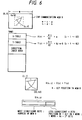
- FIG. 8 showing a prior technology, wherein shown are a CPU 1; a ROM 2 storing a program for the CPU 1; a RAM for storing data of the CPU 1; a dictionary memory 3 for fine recognition; a coarse classification unit 5; a coarse classification memory 6; a character/communication memory 8; a character extraction CPU 9; a ROM 10 storing a program for the process executed by the CPU 9; a data RAM 11 for the CPU 9; and a scanner 12 for text image entry.
- a text image is entered by the scanner into the RAM 11.
- the CPU 9 effects a character extraction process on the text image stored in the RAM 11, stores the extracted character in the character communication memory 8, and asks the CPU 1 to effect the recognition process.
- Then conducted is a smoothing process, by applying a filtering process on each of 62 x 62 pixels and 8 surrounding pixels, thereby determining the value of each pixel and removing the distortion at the normalization (Fig. 9B).
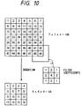
- an image of 64 x 64 pixels, including a white pixel added to each side, is divided into 7 x 7 blocks, and a histogram is formed on the number of direction patterns 1 - 4 shown in Fig. 9C, in each block. There may be made two counts, in certain cases, on the direction 2 or 4. There is thus determined a vector of 196 dimensions in total, which is reduced to a vector of 4 x 4 x 4 64 dimensions by filtering as shown in Fig. 10. Said vector of 64 dimensions constitutes a feature vector.
- the above-explained process from the normalization of character image to the determination of 64-dimensional vector constitutes the feature extraction.
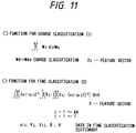
- the coarse classification unit 5 effects coarse classification by matching the above-mentioned feature vector with all the characters in the dictionary memory 6 according to an equation (1) in Fig. 11, thereby reducing the number of candidate characters to about 1/10.
- CPU 1 effects distance calculation according to an equation (2) on the candidate characters obtained in the coarse classification unit, and returns the several characters highest in the ranking, as the result of recognition, to the CPU 9 through the character communication memory 8.
- a CPU if provided exclusively for feature extraction, generally leads to a cost increase which is more significant than the achievable reduction in processing time.
- the present invention is to effect a process which is to calculate second image information from the entered first image information, to extract direction information from said second image information and to count said direction information and which has been conducted by a software, by a hardware thereby enagling parallel processing.
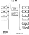
- Fig. 1A is a block diagram best representing the feature of the present invention.
- an image input/character extraction section for entering a text image from a scanner and effecting character extraction.
- a character recognition section for describing the feature of each extracted character image by a feature vector, matching the feature vector with the dictionary memory and rleasing a character of shortest distance as the candidate character.
- a CPU 1 for controlling the entire recognition unit; a ROM 2 storing programs for the CPU 1; a RAM 3 for storing the data of the CPU 1 and the feature vector; a detailed dictionary memory 4 for storing data for matching with the feature vector, for detailed distance calculation by the CPU 1 based on the candidate characters obtained from a coarse classification unit 5 to be epxlained later; a coarse classification unit 5 for effecting simple distance calculations between the feature vector and all the characters thereby selecting candidate characters; a coarse classification dictionary memory 6 storing the matching data for the coarse classification unit 5; a direction index extraction unit 7 of which structure is shown in Fig.
- a character communication memory 8 for storing a character image extracted by the character extraction section and conducting communication between the character extraction section and the recognition section; a CPU 9 for controlling the entire image input/character extraction section; a ROM 10 storing programs for the CPU 9; a data RAM 11 for storing text image for character extraction by the CPU 9; and a scanner 12 for text image input.
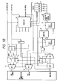
- Fig. 1B is a block diagram of the direction index extraction unit 7 shown in Fig.
- control unit 13 for internal control of said direction index extraction unit 7; latches 14 - 17; an adder 18; multiplexers 19 - 21; a white pixel masking unit 22; a 3 x 3 shift register 23; a smoothing unit 24; a 2 x 2 shift register 25; a direction index decoder unit 26; and a direction index counter 27.
- the entire process flow is as follows. At first the scanner stores the text image to be processed in the RAM 11, and the CPU 9 executes character extraction on thus stored text image. Then the CPU 9 transfers the extracted image and the position of character to the character/communication memory 8 which has, as shown in Fig. 2A, a character image area, a character position area and a recognition result area in succession from the lowermost address.
- the character image area stores, as shown in Fig. 2B, a part of the text image subjected to character extraction.
- the character position area stores, as shown in Fig.
- the rectangular image stored in the character image area may contain any number of characters as long as the product W x H of the number W of bytes in the horizontal direction and the number H of dots in the vertical direction of the rectangular image does not exceed the size of the character image area.
- the unit of transfer from the RAM 11 to the character/communication memory 8 is determined by the size of the character image area. For example, if the character image area is very small, said transfer has to be made in the unit of a character.
- the transfer may be conducted in the unit of a line, a half page, or an entire page in extreme case.
- the 2nd character can be represented by replacing a1, b1, c1, d1 mereby with a2, b2, c2, d2.
- the CPU 1 returns eight character codes positioned close in the dictionary patterns and distances from the standard patterns in said dictionary, as shown in Fig. 2D.
- the CPU 1 executes a recognition process.
- the recognition process is principally composed of three steps.
- the first step for feature extraction effects feature extraction on the designated character position of the given image, thereby extracting a feature vector.
- the second step of coarse classification matches the feature vector obtained in the feature extraction with the standard patterns of all the characters in the coarse classification dictionary memory 6, thereby selecting candidate characters of a number which is about 1/10 of the number of all the characters (for example 50 candidate characters from 3,000 characters).
- the third step for fine recognition compares the feature vector, obtained in the feature extraction, with the content of the detailed dictionary memory 4 corresponding to the candidate characters obtained in the coarse classification, thereby reducing the number of candidate characters to several characters (8 characters in the example shown in Fig. 2D). The obtained results are supplied to the recognition result area of the character/communication memory 8.
- the character/communication memory 8 has a capacity of 128 kbytes and a 16-bit bus
- the CPU 1 has a data bus width of 32 bits and that all the addresses are counted by the unit of byte.
- the multiplexers 19, 20 in Fig. 1B are 2-tol selectors for selecting outputs in response to a signal B from the control unit 13. Normally the multiplexer 19 is selected by an address bus from the CPU while the multiplexer 20 is selected by a read/write control signal to the character/communication memory 8 from the CPU, whereby the direct read/write operation from the CPU 1 is rendered possible.
- the multiplexer 19 has to have 16 bits, based on the structure of the memory 8.
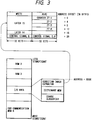
- the CPU 1 regards the character/communication memory 8 as a device of a separate address mapping from that of the direction index extraction unit 7, which has,as an I/O device, an address map as shown in Fig. 3.
- a word of the CPU 1 is of 4 bytes (32 bits), and the latch 15 is mapped over 4 words.
- a latch signal F therefor is supplied not only to the latch 15 but also to the latches 16, 17, shift registers 23, 25 and counter 27.
- the latch 15 does not latch the data from the CPU 1 but the sum of output of the latch 14 and the data from the data bus of the CPU 1, through the adder 18.
- each of the latches 14, 15 has to have 20 bits.
- the upper 16 bits are connected to the multiplexer 19, while the lower 4 bits are connected to the input ports of the latch 17.
- the latch 14 is also mapped as shown in Fig. 3, and latches the data from the data bus of the CPU 1, by a signal A from the control unit 13 in response to a writing operation of the CPU 1 in the corresponding address. Addresses of offset 20 bytes of the direction index extraction unit 7 are used for set/resetting of a signal B and are normally in the reset state.
- the output of the multiplexer 19 releases the upper 16 bits of the latch 15, thereby addressing the character/communication memory 8.
- a signal C of the control unit is supplied as a control signal for the memory 8 from the multiplexer 20, and, in this state the access from the CPU 1 to the memory 8 is inhibited.
- the data are read from the character/ communication memory 8 and are latched in the latch 16 at a same timing as the latch 15.
- Said latch 16 has a width of 16 bits, same as in the data bus of the memory 8.
- the data writing operation from the CPU 1 is conducted in the above-explained manner. In the data reading operation, the values of counters 1 - 4 of the counter unit 27 are read.
- Said counters 1 - 4 respectively correspond to the direction indexes 1 - 4.
- Pulse signals D, H are generated by a reading operation dummy reading) of the addresses of offset 20 bytes.
- the signal D is used for clearing the shift registers 23, 25, bus it masked when the signal B is set.
- the signal H is used for clearing the counters of the counter unit.
- the shift register 23 has a capacity of 12 bits x 3 rows, while the shift register 24 has a capacity of 12 bits x 2 rows. Said capacity of 12 bits is selected for the following reason.
- a normalization size of 62 x 62 pixels, with an additional pixel on each side provides a size of 64 x 64 pixels, which provides 63 x 63 direction index masks each composed of 2 x 2 pixels.
- Said 2 x 2 masks can be divided into 7 x 7 blocks each composed of 9 x 9 masks.
- Said 9 x 9 masks each composed of 2 x 2 pixels are constituted by 10 x 10 pixels, which require an additional pixel on each side for smoothing process.
- direction indexes of a block can be obtained from 12 x 12 pixels. Therefore, by entering the data of 12 x 12 pixels into the shift register of 12 bits x 3 rows in the sequence shown in Fig. 4B and obtaining outputs of 9 bits as shown in Fig.
- This control is conducted by signals E and G of the control unit 13.
- the latch 15 covers 4 words.
- the data latching in the latch 15 is conducted regardless of the values of 2-bit address signals of the lower 2 bits CPU-A0, CPU-A1 of the address bus of the CPU 1.
- the output of the latch 15 indicates a bit in the memory 8 as explained before, and the property of said 1-bit data is indicated by said 2-bit address signals.
- a signal CPU-S0 "0" indicates that the 1-bit data in the memory 8 is a white pixel for the outer frame
- a signal CPU-S1 "1" indicates that the 1-bit data is to be supplied to the shift register 23, then subjected to the smoothing and the direction index decoding and subjected to the counting of the direction index according to the decoded value.
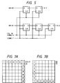
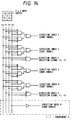
- the signals E, G are generated by a circuit shown in Fig. 5, in which as in the shift register unit, the signal D clears the register and the signal F causes 1-bit shift.
- the signal E is delayed by two cycles from the signal F. More specifically, when the bit address for the pixel No. 1 shown in Fig.
- the counting is not possible for a pixel No. 27 in Fig. 4B because a 4 x 4 mask contemplated from said pixel overflows the frame of 12 x 12 pixels, while the counting is possible for a pixel No. 144 since a 4 x 4 mask contemplated from said pixel is included in the frame of 12 x 12 pixels.
- the counter unit 27 effects the counting operation, receiving the signal G representing said counting property and the output of the direction index decoding unit 26.
- each of the counters 27-2 and 27-4 is capable of selecting a +1 count or a +2 count.
- the latch 14 and the adder 18 function in the following manner.
- the CPU 1 receives the parameters of the character position from the character/communication memory 8 and prepares tables of X(x) and Y(y) as shown in Fig. 6.
- the bit position in the character/ communication memory 8 corresponding to the coordinate (x, y) of the normalized character image, is represented by X(x) + Y(y).
- the data X(1) is latched in the latch 14, and, when the latching of data Y(1) in the latch 15 is tried, the latch 15 stores the bit position of the character/communication memory 8 corresponding to the coordinate (1, 1) of the normalized character image.
- the direction index extraction unit 7 effects the necessary process.
- the CPU 1 only executes the preparation of the X- and Y-tables and the transfer of data thereof to the latch 14 and, with the aforementioned property, to the latch 15.
- the values of the counters 1 - 4 of the counter unit 27 are read and stored in the RAM 3, then said counters are cleared by the signal H, and there can be conducted the data transfer of a next block.
- the process time for a pixel of a normalized image can be made approximately equal to the transfer time from the RAM 3 to the latch.
- the pixel data are transferred in the vertical sequence as shown in Fig. 4B, because the 7 x 7 blocks are assumed to be numbered as shown in Fig. 7A.
- the numbering arrangement as shown in Fig. 7A it is natural to process the blocks in the order of 1, 2, 3, 4, 5, ...
- 12 x 12 pixels are required for obtaining 9 x 9 direction indexes. Stated differently, there are required additional processings.
- the pixel data are transferred in the vertical sequence, there are only required 12 x 9 pixels for the block 2 since it is continuation of the block 1.
- the direction indexes can be read in the order of 1, 2, 3 and 4 by reading the values of the counters in a sequence of 3, 4, 1 and 2 in the counter unit 27.
- a high-speed extraction of direction indexes without the necessity of rearrangement thereof can be achieved by the selection of image scanning direction (pixel transfer direction) according to the desired output format (sequential order of 7 x 8 blocks).
- the direction indexes are extracted from the blocks shown in Fig. 7B with the scanning direction shown in Fig. 7A, the process becomes complicated since it is necessary to rearrange the 196-dimensional vector according to the arrangement shown in Fig. 7B or to effect the data transfer from the counter unit 27 to the RAM 3 shown in Fig. 1 so as to match the block arrangement shown in Fig. 7B.
- the circuit shown in Fig. 1B has a 4-stage pipeline structure. More specifically, the data in the character/communication memory 8 can be processed in the counter unit 27 only after three other data are latched in the latch 15. Thus, in order to obtain 9 x 9 direction indexes, at first pixels 1 - 36 are transferred with counting inhibited. In each of subsequently lines, 3 pixels are transferred with counting inhibited, and 9 pixels are transferred with counting permitted. After the data transfer in this manner to the pixel 144, pixels 145, 146 and 147 of the next block are transferred with counting inhibited, then the values of the counters 1 - 4 of the counter unit 27 are read, and said counters are cleared.
- the data transfer from the X, Y tables in the RAM 3 to the latches 14, 15 and the data transfer from the counter unit 27 to the RAM 3 are executed by the CPU 1, but there may be employed a DMA controller for these data transfers.
- the latch 14 holds the data X(a) of the arrangement of the X-table. Then, when the CPU 1 transfer the data Y(b) to the latch 15, the address of a pixel in the memory 8, corresponding to the normalized coordinate (a, b) is supplied to the adder 18 and to the latch 15. Then, at the next transfer of the data Y(b + 1), 1-word data in the memory 8 corresponding to the coordinate (a, b) are latched in the latch 16. Then, at the transfer of the data Y(b + 2), the pixel data of the coordinate (a, b) are selected by the output of the latch 17 and by the multiplexer 21 and masked by the signal E indicating the white frame property for the coordinate (a, b).
- the smoothing unit 24 effects smoothing on 9 pixels in total, consisting of said masked output and data of 8 pixels already stored in the 3 x 3 shift register 23, and the result of smoothing for the pixel at (a - 1, b - 1) is entered into the 2 x 2 shift register unit 25 (shift input).
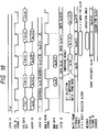
- a 2 x 2 mask is released from the shift register 25 for a 4 x 4 mask of the rectangular coordinates (a-3, b-3) - (a, b) as shown in Fig. 19, and is converted by the direction index decoding unit 26 into addition data of different directions.
- the count property signal G indicates the count inhibited or permitted state for a 2 x 2 mask with the coordinate (a, b) positioned at the lower end of 4 x 4 mask, and the counter unit 27 is controlled by the output of said decoding unit 26 and said signal G.
- the line CPU-A0 in Fig. 6 indicates a property that the coordinate (a, b) belongs to the white frame, while the line CPU-Al indicates a property whether the direction index counting is inhibited or permitted for the mask of rectangular coordinate (a-2, b-2) - (a-1, b-1).
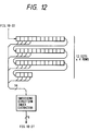
- the 3 x 3 and 2 x 2 shift registers, the smoothing unit and the direction index extraction unit shown in Fig. 1B are replaced by a structure shown in Fig. 12, in which 4 x 4 masks are generated by a shift register of 12 bits x 4 rows, and 3 x 3 smoothing and extraction of 2 x 2 direction indexes are simultaneously conducted by a smoothing/direction index extracting unit, based on said 4 x 4 masks.
- the process executed by the CPU 1 is not at all affected by the structure shown in Fig. 12.
- the latch 14 and the adder 18 are eliminated from the structure shown in Fig. 1B.
- the hardware for white frame masking can be dispensed with by storing a white pixel in a predetermined address of the character/communication memory and making access to said address at the white frame processing.
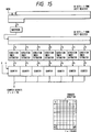
- a block size setting register and multiplexers are added, as shown in Fig. 13, to the 3 x 3 shift register and the 2 x 2 shift register in Fig. 1B.
- the block size in this embodiment is rendered variable from 9 x 9 to 16 x 16 by setting values 0 - 7 in said block size setting register.
- the number of direction indexes (2 x 2 masks) for each block is represented by (block size - 3)2.
- the normalization size N is represented by:
- N (block division number) x (block size - 3) - 1.
- the block division number is 7 while the block size is 12, so that the normalization size is 62.
- the direction index extraction unit 7 is a hardware for processing in the unit of a block, and the sequence of processing of blocks is determined by the control of the CPU 1.
- Fig. 14 shows the internal structure of the direction index decoding unit 26 shown in Fig. 1B.
- a counter 5 in the counter unit By adding a counter 5 in the counter unit and connecting said counter to a direction index 5 count enable signal, shown by a broken-lined frame in Fig. 14, the number of black pixels in each block is counted by said counter 5.
- the process of the CPU 1 is modified, in the data reading from the counter unit to the RAM 3, to the reading of index 5 instead of index 4, so that the processing time is hardly affected.
- Such structure of the direction index decoding unit and the counter unit enables extraction not only of directional feature but also of other features such as black/white pixel density.
- the processing is conducted in the unit of each of 7 x 7 blocks.
- the shift register of 12 bits x 3 rows is replaced by a shift register of 64 bits x 3 rows
- the shift register of 12 bits x 2 rows is replaced by a shift register of 64 bits x 2 rows
- the processing time of the lst embodiment represented by 12 x 9 x (data transfer time) the present embodiment a shorter processing time of 9 x 9 x (data transfer time).
- the normalization size of 62 pixels with a white frame of two pixels therearound gives rise to 66 bits, but there can be adopted 64 bits by omission of two pixels, as two pixels on each end are white pixels.
- the normalization size and the number of block division are fixed.
- the white frame is processed by the address signal of the CPU 1, but this method requires to vary the processing of the CPU 1 for a block containing the white frame and for a block not containing such white frame.
- This embodiment employs a size of 66 x 66 pixels, including the white frame added to the normalization size.
- the X, Y-tables shown in Fig. 6 are prepared in range of X(-1) - X(64) and Y(-1) - Y(64), and white pixel information is set in the data of X(-1), X(0), X(63), Y(-1), Y(0), Y(63) and Y(64).
- the pixels are regarded as belonging to the white frame when the sum of X and Y exceeds said maximum capacity.
- the data bus of the CPU 1 is of 32 bits
- a value "0x80000000" with the most significant bit "1" is stored in X(-1), X(0), X(63), X(64), Y(-1), Y(0), Y(63) and Y(64)
- the white frame masking signal generator shown in Fig. 5 is modified as shown in Fig. 16.
- the white frame process is automatically executed by the data X(-1), ..., X(64), Y(-1), ..., Y(64), so that the CPU 1 can execute same processing for all the blocks.
- the property or attribute of the pixel is processed by the address signal of the CPU 1.
- an attribute setting register is provided, as shown in Fig. 17, in the control unit 13 shown in Fig. 1B, and the property is recorded in said register whenever it is varied.
- the structure is same as shown in Figs. 1A and 1B, but the image from the scanner 12 is not stored in the RAM 11 but in the character/communication memory 8, and the CPU 9 executes character extraction on the text image stored in said memory 8.
- the scanner is of A4 size with a resolving power of 400 dbi, there is required a capacity of about 2 MBytes or 224 bits. This capacity can be processed without problem if the latches 14, 15 and the adder 18 in Fig. 1B have a bit width of 24 bits of larger.
- the CPU 9 is incapable of character extraction during the access of the recognition section to the memory 8, but said access takes place only at the preparation of X, Y-tables in the RAM 3, the direction index extraction in each block, and the output of result of recognition, but not during the preparation of 64-dimensional feature vector from the 196-dimensional direction indexes, the coarse classification and the detailed recognition.
- the lst embodiment also requires image transfer time from the RAM 3 to the memory 8, there is no deterioration in performance if the access period of the recognition section to the memory 8 does not exceed the above-mentioned image transfer time.
Landscapes
- Engineering & Computer Science (AREA)
- Computer Vision & Pattern Recognition (AREA)
- Physics & Mathematics (AREA)
- General Physics & Mathematics (AREA)
- Multimedia (AREA)
- Theoretical Computer Science (AREA)
- Character Input (AREA)
- Character Discrimination (AREA)
Applications Claiming Priority (3)
| Application Number | Priority Date | Filing Date | Title |
|---|---|---|---|
| JP206619/90 | 1990-08-03 | ||
| JP20661990 | 1990-08-03 | ||
| JP2206619A JPH0492993A (ja) | 1990-08-03 | 1990-08-03 | 文字認識装置 |
Publications (3)
| Publication Number | Publication Date |
|---|---|
| EP0471473A2 true EP0471473A2 (fr) | 1992-02-19 |
| EP0471473A3 EP0471473A3 (en) | 1993-11-03 |
| EP0471473B1 EP0471473B1 (fr) | 2000-03-08 |
Family
ID=16526377
Family Applications (1)
| Application Number | Title | Priority Date | Filing Date |
|---|---|---|---|
| EP91307006A Expired - Lifetime EP0471473B1 (fr) | 1990-08-03 | 1991-07-31 | Appareil et méthode de reconnaissance d'image |
Country Status (3)
| Country | Link |
|---|---|
| EP (1) | EP0471473B1 (fr) |
| JP (1) | JPH0492993A (fr) |
| DE (1) | DE69132019T2 (fr) |
Cited By (1)
| Publication number | Priority date | Publication date | Assignee | Title |
|---|---|---|---|---|
| WO2000063833A1 (fr) * | 1999-04-15 | 2000-10-26 | Electronics For Imaging, Inc. | Detection intelligente d'un texte sur une page |
-
1990
- 1990-08-03 JP JP2206619A patent/JPH0492993A/ja active Pending
-
1991
- 1991-07-31 EP EP91307006A patent/EP0471473B1/fr not_active Expired - Lifetime
- 1991-07-31 DE DE69132019T patent/DE69132019T2/de not_active Expired - Fee Related
Non-Patent Citations (5)
| Title |
|---|
| INT CONF ON ACOUSTICS, SPEECH AND SIGNAL PROCESSING vol. 2, 11 April 1988, NYC, NEW YORK pages 1056 - 9 .F. CATTHOOR AND AL. 'An ASIC architecture for contour line filtering' * |
| OPTICAL ENGINEERING vol. 28, no. 7, July 1989, BELLINGHAM, WA pages 793 - 9 B. JENG 'Optical chinese character recognition using accumulated stroke features' section 2. * |
| PROC. CVPR '85 1985, pages 550 - 7 I. MASUDA, N. HAGITA ET AL 'Approach to Smart Document Reader System' section 4.1 * |
| PROC. INT. CENTER FOR THEORITICAL PHYSICS 1983, pages 169 - 74 H. HAGITA, I. MASUDA ET AL. 'Handprinted Kanji character recognition based on pattern matching method' section 2. * |
| PROC. OF THE 1987 IEEE INT. CONF. ON SYSTTEMS, MAN, AND CYBERNETICS vol. 2, 20 October 1987, ALEXANDRIA, VA pages 759 - 63 O. IWAKI ET AL 'a segmentation method based on office document hierarchical structure' section 5.2 * |
Cited By (2)
| Publication number | Priority date | Publication date | Assignee | Title |
|---|---|---|---|---|
| WO2000063833A1 (fr) * | 1999-04-15 | 2000-10-26 | Electronics For Imaging, Inc. | Detection intelligente d'un texte sur une page |
| US6289122B1 (en) | 1999-04-15 | 2001-09-11 | Electronics For Imaging, Inc. | Intelligent detection of text on a page |
Also Published As
| Publication number | Publication date |
|---|---|
| DE69132019D1 (de) | 2000-04-13 |
| EP0471473B1 (fr) | 2000-03-08 |
| EP0471473A3 (en) | 1993-11-03 |
| DE69132019T2 (de) | 2000-08-31 |
| JPH0492993A (ja) | 1992-03-25 |
Similar Documents
| Publication | Publication Date | Title |
|---|---|---|
| US4750209A (en) | System for processing an image having both letter and photographic information | |
| US4153897A (en) | Method and device for detecting the similarity between standard and unknown patterns | |
| US4653107A (en) | On-line recognition method and apparatus for a handwritten pattern | |
| EP0154449B1 (fr) | Système d'amincissement de caractères en temps réel | |
| US5307422A (en) | Method and system for identifying lines of text in a document | |
| EP0173098A2 (fr) | Procédé et appareil pour suivre le contour d'une forme | |
| JP2766053B2 (ja) | 画像データ処理方法 | |
| EP0524797A2 (fr) | Procédé et appareil de traitement d'image | |
| US5253305A (en) | Character boundary identification method and system | |
| EP0471472B1 (fr) | Appareil et procédé de traitement d'image | |
| EP0744711A2 (fr) | Méthode et appareil pour rotation d'image | |
| US4138662A (en) | Character reader | |
| EP0471473B1 (fr) | Appareil et méthode de reconnaissance d'image | |
| EP0114305B1 (fr) | Normalisation des signaux d'image de caractères imprimés | |
| US5623556A (en) | System and method of extracting binary image data | |
| CA2250557C (fr) | Methode de reconnaissance d'images a interpretation localisee | |
| Misra et al. | A memory efficient method for fast transposing run-length encoded images | |
| JP3072126B2 (ja) | 書体を識別する方法及び装置 | |
| JP2774113B2 (ja) | 文字認識方法 | |
| JP3046711B2 (ja) | 相関演算装置 | |
| JP2917396B2 (ja) | 文字認識方式 | |
| KR900007727B1 (ko) | 문자 인식 장치 | |
| JP2868533B2 (ja) | 図面読み取り装置 | |
| JP2940974B2 (ja) | マッチング方法 | |
| WO1990001750A1 (fr) | Processeur d'images a balayage intelligent |
Legal Events
| Date | Code | Title | Description |
|---|---|---|---|
| PUAI | Public reference made under article 153(3) epc to a published international application that has entered the european phase |
Free format text: ORIGINAL CODE: 0009012 |
|
| AK | Designated contracting states |
Kind code of ref document: A2 Designated state(s): DE FR GB |
|
| PUAL | Search report despatched |
Free format text: ORIGINAL CODE: 0009013 |
|
| AK | Designated contracting states |
Kind code of ref document: A3 Designated state(s): DE FR GB |
|
| 17P | Request for examination filed |
Effective date: 19940321 |
|
| 17Q | First examination report despatched |
Effective date: 19950322 |
|
| GRAG | Despatch of communication of intention to grant |
Free format text: ORIGINAL CODE: EPIDOS AGRA |
|
| GRAG | Despatch of communication of intention to grant |
Free format text: ORIGINAL CODE: EPIDOS AGRA |
|
| GRAG | Despatch of communication of intention to grant |
Free format text: ORIGINAL CODE: EPIDOS AGRA |
|
| GRAH | Despatch of communication of intention to grant a patent |
Free format text: ORIGINAL CODE: EPIDOS IGRA |
|
| GRAH | Despatch of communication of intention to grant a patent |
Free format text: ORIGINAL CODE: EPIDOS IGRA |
|
| GRAA | (expected) grant |
Free format text: ORIGINAL CODE: 0009210 |
|
| AK | Designated contracting states |
Kind code of ref document: B1 Designated state(s): DE FR GB |
|
| REF | Corresponds to: |
Ref document number: 69132019 Country of ref document: DE Date of ref document: 20000413 |
|
| ET | Fr: translation filed | ||
| PLBE | No opposition filed within time limit |
Free format text: ORIGINAL CODE: 0009261 |
|
| STAA | Information on the status of an ep patent application or granted ep patent |
Free format text: STATUS: NO OPPOSITION FILED WITHIN TIME LIMIT |
|
| 26N | No opposition filed | ||
| PGFP | Annual fee paid to national office [announced via postgrant information from national office to epo] |
Ref country code: GB Payment date: 20010717 Year of fee payment: 11 |
|
| PGFP | Annual fee paid to national office [announced via postgrant information from national office to epo] |
Ref country code: FR Payment date: 20010720 Year of fee payment: 11 |
|
| PGFP | Annual fee paid to national office [announced via postgrant information from national office to epo] |
Ref country code: DE Payment date: 20010927 Year of fee payment: 11 |
|
| REG | Reference to a national code |
Ref country code: GB Ref legal event code: IF02 |
|
| PG25 | Lapsed in a contracting state [announced via postgrant information from national office to epo] |
Ref country code: GB Free format text: LAPSE BECAUSE OF NON-PAYMENT OF DUE FEES Effective date: 20020731 |
|
| PG25 | Lapsed in a contracting state [announced via postgrant information from national office to epo] |
Ref country code: DE Free format text: LAPSE BECAUSE OF NON-PAYMENT OF DUE FEES Effective date: 20030201 |
|
| GBPC | Gb: european patent ceased through non-payment of renewal fee |
Effective date: 20020731 |
|
| PG25 | Lapsed in a contracting state [announced via postgrant information from national office to epo] |
Ref country code: FR Free format text: LAPSE BECAUSE OF NON-PAYMENT OF DUE FEES Effective date: 20030331 |
|
| REG | Reference to a national code |
Ref country code: FR Ref legal event code: ST |