EP0471626B1 - Vorrichtung zur Speisung und Regelung des Stromes für den Kathodenglühfaden einer Röntgenröhre - Google Patents
Vorrichtung zur Speisung und Regelung des Stromes für den Kathodenglühfaden einer Röntgenröhre Download PDFInfo
- Publication number
- EP0471626B1 EP0471626B1 EP91402249A EP91402249A EP0471626B1 EP 0471626 B1 EP0471626 B1 EP 0471626B1 EP 91402249 A EP91402249 A EP 91402249A EP 91402249 A EP91402249 A EP 91402249A EP 0471626 B1 EP0471626 B1 EP 0471626B1
- Authority
- EP
- European Patent Office
- Prior art keywords
- circuit
- current
- output
- filament
- signal
- Prior art date
- Legal status (The legal status is an assumption and is not a legal conclusion. Google has not performed a legal analysis and makes no representation as to the accuracy of the status listed.)
- Expired - Lifetime
Links
Images


Classifications
-
- H—ELECTRICITY
- H05—ELECTRIC TECHNIQUES NOT OTHERWISE PROVIDED FOR
- H05G—X-RAY TECHNIQUE
- H05G1/00—X-ray apparatus involving X-ray tubes; Circuits therefor
- H05G1/08—Electrical details
- H05G1/10—Power supply arrangements for feeding the X-ray tube
- H05G1/20—Power supply arrangements for feeding the X-ray tube with high-frequency AC; with pulse trains
-
- H—ELECTRICITY
- H05—ELECTRIC TECHNIQUES NOT OTHERWISE PROVIDED FOR
- H05G—X-RAY TECHNIQUE
- H05G1/00—X-ray apparatus involving X-ray tubes; Circuits therefor
- H05G1/08—Electrical details
- H05G1/26—Measuring, controlling or protecting
- H05G1/30—Controlling
- H05G1/34—Anode current, heater current or heater voltage of X-ray tube
Definitions
- the invention relates to a device for supplying current to a filament of a cathode of an X-ray tube and for regulating said current to a selected value.
- An X-ray tube is generally made up like a diode, that is to say by two electrodes of which one, called cathode, emits electrons while the other, called anode, receives these electrons on a small surface which constitutes the X-ray source.
- the cathode has a heated filament which is the source of electrons.
- a so-called anodic current is established through the generator and crosses the space between the cathode and the anode in the form of an electron beam whose intensity depends on the temperature of the filament, this temperature being a function of the power dissipated in the filament, that is to say of the current, called the heating current, flowing through the filament.
- the quantity of X-rays emitted by the anode depends mainly on the intensity of the anode current and therefore on the heating current of the filament. Also, the filament heating current constitutes one of the important parameters which must be determined for each exposure of radiography or radioscopy during an X-ray examination of a patient.
- the parameters of the pose are determined according to the nature of the examination. Generally, these parameters are predetermined by an operator who displays the values on a control panel through which controlled the operation of the various organs of a radiology installation such as, for example, the high voltage generator and the generator of the filament heating current. More and more often, the values of these parameters are determined using a microprocessor device which calculates and programs the optimal values of these parameters according to, for example, the type of examination desired by the practitioner and the specific characteristics of the installation.
- the parameters which are calculated and programmed are, for example, the duration of the exposure time, the energy of the X-ray by the choice of the value of the high voltage applied between the cathode and the anode and the intensity of the anode current. by the choice, in particular, of a value of the intensity of the heating current of the filament.
- the intensity of the heating current must be able to be modified significantly, from one pose to the next, for example from 1.5 amperes to 5.5 amperes but also during the same pose.
- these current values must be obtained quickly and automatically and be maintained for the required time.
- the power supply circuit 11 comprises a DC voltage source 13 represented by a battery 13 ′ and an inverter circuit 14.
- the inverter circuit 14 comprises a chopper circuit 31 comprising switches 20 and 21 controlled by a control circuit 19 and diodes 22 and 23, and a resonant circuit 10 comprising the capacitors 24 and 25 and the coil 26.
- the resonant circuit 10 is connected to a primary winding 28 of an isolation transformer 9 of which the secondary circuit 27 comprises the filament 15 of the cathode of the X-ray tube 30.
- the filament 15 is optionally supplied via a rectifier circuit 29 which is for example of the type with diodes and filtering capacitor.
- the regulating circuit 12 comprises a circuit 8 for detecting the heating current of the filament and a circuit 16 for measuring this heating current of the filament, a circuit 17 for comparing the current measured with a predetermined value, called the reference value, a converter circuit 18 variable voltage-frequency which is applied to the inverter circuit 14 so as to modify the frequency and thus obtain a heating current whose value is equal to a set value Ic.
- the device which has just been described succinctly has the following drawbacks.
- the sudden blockage of the transistors of the switches 20 and 21 of the inverter circuit 14 gives rise to rapid variations in the current which create parasitic signals, the latter disturbing the surrounding circuits and, in particular, the primary circuit 28 of the transformer which includes the detection circuit. 8 of the heating current.
- the measurement signals therefore comprise parasites which create an error in the regulation circuit 12. When this error is reproducible, it can be corrected by calibrating the device.
- the sudden blockage of the transistors of the inverter circuit 14 also has the effect that the current flowing in the filament 15 has a shape that evolves between the sinusoid and the sawtooth when the voltage E of the source varies.
- the heating current approaches the sawtooth, its value squared presents peaks which correspond to harmonics of high rank which the circuit for measuring the effective value cannot reproduce because its bandwidth is insufficient.
- An object of the present invention is therefore to provide a supply circuit in which the operating phases of the inverter circuit do not include a sudden blockage of the current in the semiconductors, nor a waveform of filament current having high harmonics.
- the invention provides an inverter circuit of the hyporesonant type with discontinuous operation in which the switching frequency of the semiconductor of the inverter circuit is lower than the resonance frequency of the resonant circuit and in which the switching of the semiconductor is performed when the current in them is zero.
- any filtering in the measurement chain is equivalent to a derivation in the direct chain, derivation which is source of instability.
- the direct chain includes a filtering which greatly limits the bandwidth of the servo loop, which results in the delay indicated above.
- Another object of the present invention is therefore to produce a regulation circuit which does not include a filtering circuit in the measurement chain.
- the measurement signal is raised from the square and is compared to the square value of a setpoint and it is therefore not necessary to use a circuit for calculating the square root which would include a circuit for filtering.
- FIG. 1 The diagram of FIG. 1 has been described succinctly in the preamble to show certain drawbacks of the devices for feeding and regulating the filament current of X-ray tubes according to the prior art.
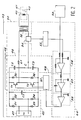
- the device for supplying and regulating the current of a cathode filament 40 of an X-ray tube 41 comprising an anode 42 comprises a current supply circuit 43 and a circuit 44 for regulating the current flowing in the filament 40.
- the power supply circuit 43 includes a DC voltage source 45, an inverter circuit 46 and an isolation transformer 50.
- the DC voltage source 45 can be of any known type without voltage regulation. It includes, for example, a source 47 of alternating voltage which is connected to diodes D1 to D4 mounted as a full-wave rectifier bridge. The output terminals of the rectifier bridge are connected to the inverter circuit 46 by means of a filter cell which mainly consists of an electrolytic capacitor C1.
- the inverter circuit 46 comprises a chopping circuit 48 and a resonant circuit 49.
- the chopping circuit 48 comprises, for example, two field effect transistors T1 and T2 which are connected in series on the output terminals of the supply circuit 45 and two diodes D5 and D6 which are respectively connected in parallel between the drain and the source of transistors T1 and T2, the outputs of which are each connected to the control gate of transistor T1 or T2 so that their anode is connected to the source of the corresponding transistor. It also includes a control circuit 51 of the transistors T1 and T2.
- the resonant circuit 49 comprises, for example, two capacitors C2 and C3 which are connected in series on the output terminals of the inverter circuit 48 and a coil L1, one terminal of which is connected directly to the anode of the diode D5 and whose another terminal is connected, via a primary winding 52 of the transformer 50, to the common point C of the capacitors C2 and C3.
- the isolation transformer 50 of the pulse type, comprises, in addition to the primary winding 52, a secondary winding 53 whose output terminals are connected directly to the filament 40 of the cathode of the X-ray tube 41. It should be noted that, with respect to the diagram in FIG. 1, there is no rectifier circuit in the secondary circuit so that the filament 40 is supplied with pulse current. However, the device according to the invention can be implemented in the case where a rectifier circuit is connected between the secondary winding 53 and the filament 40.
- the inverter circuit 46 is of the hyporesonant type, that is to say that the switching frequency of the transistors T1 and T2, as defined by the control circuit 51, is less than the resonance frequency of the resonant circuit 49.
- the regulation circuit 44 includes a circuit 54 for detecting and measuring the heating current I (t) which is connected, for example, in the primary circuit 52 of the transformer 50.
- the signal detected by this measurement circuit is applied to a multiplier circuit 55 which multiplies the input signal proportional to I (t) by itself so that the signal at the output is proportional to I2 (t).
- the output signal proportional to I2 (t) is applied to an input of a differentiator circuit 56 which also receives, on its other input, a reference signal I2 ref corresponding to the current I ref which it is desired to obtain in the filament 40.
- This signal I2 ref is supplied by a control device 59.
- the signal error ⁇ I2 ref - I2 (t) is applied to an integrator circuit 57 whose output signal is applied to a comparator 58 whose reference potential is ground.
- the comparator 58 supplies a pulse as soon as the integrated signal is, for example, greater than the ground potential and this pulse lasts until the moment when said integrated signal becomes lower than the ground potential.
- This pulse supplied by the comparator 58, is applied to the control circuit 51 to trigger the conduction of one or the other transistor T1 or T2 depending on whether the transistor which was previously conductive was T2 or T1.
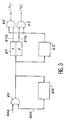
- FIG. 3 is a simplified block diagram of the control circuit 51; the latter comprises an AND logic circuit 60 of which an input 60-a is connected to the output of the comparator circuit 58 and of which the other input 60-b is connected to a delay circuit 64.
- the output of the AND circuit 60 is connected, d on the one hand, at an input of a bistable circuit 61 and, on the other hand, at the input of two delay circuits, one referenced 64 and the other referenced 65.
- the bistable circuit 61 has two outputs 61- a and 61-b, the first corresponding to state 1 and the second to state 0 , which are connected respectively to one of the two inputs of AND logic circuits 62 and 63.
- the other input of AND circuits 62 and 63 is connected to the output of the delay circuit 65.
- the AND circuit 60 provides a state change control pulse of the bistable circuit 61 each time circuit 58 supplies a pulse and a certain time or delay ⁇ 1 has elapsed since the last pulse. This delay ⁇ 1 is obtained using the delay circuit 64.
- the bistable circuit 65 supplies the control signals of the transistors T1 and T2 via the AND circuits 62 and 63, the opening of which is controlled by the signal of the delay circuit 65 which fixes the minimum duration of conduction ⁇ 2 of said transistors.
- ⁇ 1 and ⁇ 2 can be 50 microseconds and 37 microseconds respectively if the maximum switching frequency is 20 kilohertz.
- FIGS. 2, 3 and 4 assuming that a pulse T′1, (FIG. 4-g) is applied to the time t o to the control electrode of transistor T1.
- This pulse T′1 turns on and keeps the transistor T1 conductive and a current i figure (figure 4-a) says positive, flows in the transistor T1, the coil L1, the primary winding 52 of the transformer 50, the capacitors C2 and C3 and source 45 (in fact i1 / 2 in each capacitor).
- This current i1 gives rise to a tension V (figure 4-b) of sinusoidal shape at the terminals of the primary winding 52 and it results from it a current I (t) (figure 4-c) in the secondary winding 53 of the transformer 50, current of identical appearance to the current i1 flowing in the primary winding.
- the current i1 charges the capacitor C3 and discharges the capacitor C2 from the resonant circuit and their charging voltage is opposed to the circulation of the current i1 so that the latter is canceled out at time t1.
- Capacitor C3 then discharges while capacitor C2 discharges load and a current i2 (figure 4-a), said negative, circulates in the capacitors C2 and C3 (in fact i2 / 2 in each capacitor), the primary winding 52, the coil L1 the diode D5 and the source 45.
- a pulse T′2 is applied to the control electrode of the transistor T2 at the time t ′ o to make it conductive.
- a current i′1 said to be negative, then flows in the transistor T2, the source 45, the capacitors C2 and C3 (in fact i′1 / 2 in each capacitor), the primary winding 52 of the transformer 50 and the coil L1 .
- This negative current gives rise to a negative voltage V (figure 4-b) at the terminals of the primary winding 52 and this results in a negative current I (t) (figure 4-c) in the secondary winding 53 of the transformer 50 , current of identical appearance to the current i′1 flowing in the primary winding.
- the negative current i′1 charges the capacitor C2 and discharges the capacitor C3 and their charging voltage is opposed to the circulation of the current i′1 so that the latter is canceled out at time t′1.
- the capacitor C2 then discharges while the capacitor C3 charges and a positive current i′2 flows in the capacitors C2 and C3 (in fact i′2 / 2 in each capacitor), the primary winding 52, the coil L1, the diode D6 and the source 45.
- This positive current gives rise to a positive tension (figure 4-b) at the terminals of the primary winding 52 and, consequently, to a positive current I (t) (figure 4-c) in the secondary winding 53.
- the control circuit 51 operates in the following manner, assuming that the transistor which has just been conductive is the transistor T2.
- the circuit 58 provides the pulse 70 (figure 4-f)
- its front edge controls the change of state (setting to state 1) of the bistable circuit 61 via the AND circuit 60 provided that the second input of this AND circuit receives the authorization signal 71 (figure 4-h) given by the delay circuit 64.
- the signal supplied by the AND circuit 60 resets the two delay circuits 64 and 65 to zero so that the AND circuit 60 closes during time ⁇ 1 (figure 4-h) and that the circuits ET 62 and 63 open during time ⁇ 2 (figure 4-g).
- the AND circuit 62 which receives the status signal 1 from the bistable circuit 61, supplies a signal which makes the transistor T1 conductive.
- the duration of this signal is determined by the duration ⁇ 2 of the signal T′1 supplied by the delay circuit 65, that is to say at least equal to the half-period of the maximum frequency switching, so that the transistor T1 (or T2) is maintained in the conductive state for the time ⁇ 2.
- the signal T′1 (or T′2) therefore always ends after the instant t1 (or t′1).
- the delay circuit 64 provides a signal 71 ′ for opening the AND circuit 60 so that the next pulse 70 ′ changes the state of the bistable circuit 61 which changes to state 0 , ends signal 71 ′ through the circuit retarder 64 and supplies the signal T′2 via the retarder circuit 65.
- the AND circuit 63 then supplies a signal of duration ⁇ 2 which makes the transistor T2 conductive.
- the transistor T1 will be conductive because the bistable circuit 61 will return to state 1.
- the control circuit 51 described in relation to FIG. 3 comprises two delay circuits 64 and 65 but it is understood that they can be produced using a single delay circuit.
- the regulation of the current value is obtained by alternating current pulses which are substantially identical but inverse to each cycle but whose frequency varies to obtain the desired value I ref .
- I ref increases the difference ⁇ will increase and the slope (part 73-fig. 4-e) of the integrated signal will also increase so that the pulse 70 ′ will appear a little earlier and therefore trigger the transistor T2 earlier.
Landscapes
- Health & Medical Sciences (AREA)
- General Health & Medical Sciences (AREA)
- Toxicology (AREA)
- X-Ray Techniques (AREA)
Claims (3)
- Vorrichtung zur Speisung und Regelung des Stroms für den Kathodenglühfaden (40) einer Röntgenröhre (41) mit einer Stromspeiseschaltung (43) für den Glühfaden, die folgendes aufweist:- eine Wechselrichterschaltung (46) des Typs mit Halbleitern, um Stromimpulse aus einer Gleichspannungsquelle (45) zu erhalten,- eine Regelungsschaltung, die Hochfrequenzimpulse liefert, um die Halbleiter der Wechselrichterschaltung (46) zu steuern,- einen Trenntransformator (50), dessen Primärwicklung (52) mit dem Ausgang der Wechselrichterschaltung (46) verbunden ist; dadurch gekennzeichnet, daß- die Wechselrichterschaltung (46) vom hyporesonanten Typ mit diskontinuierlicher Funktionsweise ist, bei dem die Umschaltfrequenz der Halbleiter der Wechselrichterschaltung unter der Resonanzfrequenz des Resonanzkreises liegt, und bei dem die Umschaltung der Halbleiter bewirkt wird, wenn der Strom in diesen Null ist, wobei die Wechselrichterschaltung Stromimpulse an den Trenntransformator (50) liefert, und- der Trenntransformator (50) vom Impulstyp eine Sekundärwicklung (53) aufweist, die direkt mit dem Glühfaden (40) der Kathode verbunden ist.
- Vorrichtung nach Anspruch 1, dadurch gekennzeichnet, daß die Regelschaltung (44) aufweist:- eine Erfassungsschaltung (54) für den Strom I(t) in dem Glühfaden (40),- eine Schaltung (55) zum Berechnen des Quadrats I²(t) des Stroms I(t),- eine Differenzschaltung (56) zum Erhalt der Differenz ε zwischen I²(t) und einem Signal I²ref, das das Quadrat des in dem Glühfaden (40) zu erhaltenden Stroms Iref darstellt,- eine Integratorschaltung (59) für die Differenz ε,- eine Komparatorschaltung (58) zum Vergleich des integrierten Signals mit einem Schwellenwert und zum Erhalt eines Ausgangssignals, sobald das integrierte Signal den Schwellenwert überschreitet,- eine Steuerschaltung (51) für die Wechselrichterschaltung (46), die von dem Ausgangssignal der zweiten Komparatorschaltung (68) gesteuert ist und Steuersignale für die Schalter (T1, T2) der Wechselrichterschaltung (46) liefert, so daß Stromimpulse in der Primärwicklung (52) des Transformators erzeugt werden.
- Vorrichtung nach Anspruch 2, dadurch gekennzeichnet, daß die Steuerschaltung (51) folgendes aufweist:- eine erste UND-Schaltung (60), deren einer von zwei Eingängen mit dem Ausgang der zweiten Komparatorschaltung (58) verbunden ist,- eine bistabile Schaltung (61), deren Steuereingang mit dem Ausgang der ersten UND-Schaltung (60) so verbunden ist, daß sie den Zustand bei jedem von dieser gelieferten Signal verändert,- eine zweite UND-Schaltung (62), von der einer ihrer beiden Eingängen mit dem dem Zustand 1 entsprechenden Ausgang der bistabilen Schaltung (61) verbunden ist,- eine dritte UND-Schaltung (63), von der einer ihrer beiden Eingängen mit dem dem Zustand 0 entsprechenden Ausgang der bistabilen Schaltung (61) verbunden ist,- eine erste Verzögerungsschaltung (64), deren Eingang mit dem Ausgang der ersten UND-Schaltung (60) und deren Ausgang mit dem zweiten Eingang der ersten UND-Schaltung (60) verbunden ist, und- eine zweite Verzögerungsschaltung 65, deren Eingang mit dem Ausgang der ersten UND-Schaltung (60) und deren Ausgang mit dem anderen Eingang der zweiten und der dritten UND-Schaltung (62, 63) verbunden ist.
Applications Claiming Priority (2)
| Application Number | Priority Date | Filing Date | Title |
|---|---|---|---|
| FR9010349A FR2666000B1 (fr) | 1990-08-14 | 1990-08-14 | Dispositif d'alimentation et de regulation en courant d'un filament de cathode d'un tube radiogene. |
| FR9010349 | 1990-08-14 |
Publications (2)
| Publication Number | Publication Date |
|---|---|
| EP0471626A1 EP0471626A1 (de) | 1992-02-19 |
| EP0471626B1 true EP0471626B1 (de) | 1994-12-28 |
Family
ID=9399671
Family Applications (1)
| Application Number | Title | Priority Date | Filing Date |
|---|---|---|---|
| EP91402249A Expired - Lifetime EP0471626B1 (de) | 1990-08-14 | 1991-08-14 | Vorrichtung zur Speisung und Regelung des Stromes für den Kathodenglühfaden einer Röntgenröhre |
Country Status (4)
| Country | Link |
|---|---|
| US (1) | US5200984A (de) |
| EP (1) | EP0471626B1 (de) |
| DE (1) | DE69106273T2 (de) |
| FR (1) | FR2666000B1 (de) |
Families Citing this family (17)
| Publication number | Priority date | Publication date | Assignee | Title |
|---|---|---|---|---|
| DE4226442C1 (de) * | 1992-08-10 | 1993-10-14 | Siemens Ag | Schaltungsanordnung zur Messung des Röntgenröhrenstromes |
| US6298116B1 (en) * | 1999-07-06 | 2001-10-02 | U.S. Philips Corporation | X-ray examination apparatus |
| US7180981B2 (en) * | 2002-04-08 | 2007-02-20 | Nanodynamics-88, Inc. | High quantum energy efficiency X-ray tube and targets |
| FR2849983A1 (fr) * | 2003-01-10 | 2004-07-16 | Ge Med Sys Global Tech Co Llc | Procede de reglage du debit de rayonnement d'un tube a rayons x |
| US7016468B1 (en) * | 2003-03-12 | 2006-03-21 | Progeny, Inc. | X-ray tube preheat control |
| US8995621B2 (en) | 2010-09-24 | 2015-03-31 | Moxtek, Inc. | Compact X-ray source |
| US8526574B2 (en) | 2010-09-24 | 2013-09-03 | Moxtek, Inc. | Capacitor AC power coupling across high DC voltage differential |
| US8804910B1 (en) | 2011-01-24 | 2014-08-12 | Moxtek, Inc. | Reduced power consumption X-ray source |
| US8750458B1 (en) | 2011-02-17 | 2014-06-10 | Moxtek, Inc. | Cold electron number amplifier |
| US8792619B2 (en) | 2011-03-30 | 2014-07-29 | Moxtek, Inc. | X-ray tube with semiconductor coating |
| US8817950B2 (en) | 2011-12-22 | 2014-08-26 | Moxtek, Inc. | X-ray tube to power supply connector |
| US8761344B2 (en) | 2011-12-29 | 2014-06-24 | Moxtek, Inc. | Small x-ray tube with electron beam control optics |
| US9072154B2 (en) | 2012-12-21 | 2015-06-30 | Moxtek, Inc. | Grid voltage generation for x-ray tube |
| US9177755B2 (en) | 2013-03-04 | 2015-11-03 | Moxtek, Inc. | Multi-target X-ray tube with stationary electron beam position |
| US9184020B2 (en) | 2013-03-04 | 2015-11-10 | Moxtek, Inc. | Tiltable or deflectable anode x-ray tube |
| US9173623B2 (en) | 2013-04-19 | 2015-11-03 | Samuel Soonho Lee | X-ray tube and receiver inside mouth |
| US20170013702A1 (en) * | 2015-07-10 | 2017-01-12 | Moxtek, Inc. | Electron-Emitter Transformer and High Voltage Multiplier |
Family Cites Families (10)
| Publication number | Priority date | Publication date | Assignee | Title |
|---|---|---|---|---|
| NL7314036A (nl) * | 1973-10-12 | 1975-04-15 | Philips Nv | Gloeistroomverzorging voor een op hoogspanning ven elektronenbuis. |
| US3916251A (en) * | 1974-11-11 | 1975-10-28 | Cgr Medical Corp | Filament current regulator for rotating anode X-ray tubes |
| FR2538183A1 (fr) * | 1982-12-21 | 1984-06-22 | Thomson Csf | Systeme d'alimentation haute tension d'une charge telle que par exemple un generateur de rayons x |
| JPS6070698A (ja) * | 1983-09-27 | 1985-04-22 | Toshiba Corp | X線管フイラメント加熱装置 |
| DE3345036A1 (de) * | 1983-12-13 | 1985-06-13 | Heimann Gmbh, 6200 Wiesbaden | Schaltungsanordnung zum messen des anodenstromes in einer insbesondere symmetrisch betriebenen roentgenstrahlroehre |
| US4797908A (en) * | 1984-09-14 | 1989-01-10 | Kabushiki Kaisha Toshiba | Voltage-resonance type power supply circuit for X-ray tube |
| FR2577373B1 (fr) * | 1985-02-12 | 1995-02-17 | Thomson Cgr | Alimentation haute tension continue, notamment pour emetteur de rayons x |
| US4694480A (en) * | 1985-07-30 | 1987-09-15 | Kevex Corporation | Hand held precision X-ray source |
| FR2597285B1 (fr) * | 1986-04-11 | 1988-06-17 | Thomson Cgr | Dispositif d'alimentation en courant d'un filament de tube radiogene |
| FR2629959B1 (fr) * | 1988-04-08 | 1994-02-11 | Thomson Cgr | Procede de regulation de la tension d'un signal de tension, notamment pour tube a rayons x |
-
1990
- 1990-08-14 FR FR9010349A patent/FR2666000B1/fr not_active Expired - Fee Related
-
1991
- 1991-08-13 US US07/744,416 patent/US5200984A/en not_active Expired - Lifetime
- 1991-08-14 EP EP91402249A patent/EP0471626B1/de not_active Expired - Lifetime
- 1991-08-14 DE DE69106273T patent/DE69106273T2/de not_active Expired - Fee Related
Also Published As
| Publication number | Publication date |
|---|---|
| FR2666000B1 (fr) | 1996-09-13 |
| DE69106273D1 (de) | 1995-02-09 |
| EP0471626A1 (de) | 1992-02-19 |
| FR2666000A1 (fr) | 1992-02-21 |
| US5200984A (en) | 1993-04-06 |
| DE69106273T2 (de) | 1995-05-18 |
Similar Documents
| Publication | Publication Date | Title |
|---|---|---|
| EP0471626A1 (de) | Vorrichtung zur Speisung und Regelung des Stromes für den Kathodenglühfaden einer Röntgenröhre | |
| CA2250098C (en) | Method and apparatus for charging batteries | |
| EP0653692B1 (de) | Vorrichtung und Verfahren zur Regelung der Leistungsversorgung einer Batteriestromversorgung | |
| JP3499941B2 (ja) | 太陽光発電装置 | |
| KR100757320B1 (ko) | 태양광 발전 시스템의 센스리스 엠피피티(mppt)제어장치 및 그 방법 | |
| FR2629975A1 (fr) | Appareil et procede de chauffage par haute frequence, ayant une fonction de changement de la puissance de consommation nominale | |
| FR2527889A1 (fr) | Procede et appareil de reduction des harmoniques dans les circuits ballasts de lampe a decharge dans les gaz | |
| EP1334551A1 (de) | Spannungswandler mit selbstschwingender steuerschaltung | |
| FR2980653A1 (fr) | Generateur de signaux de courant et procede de mise en oeuvre d'un tel generateur | |
| FR2768273A1 (fr) | Dispositif de conversion de l'energie a butee auto-adaptive et son procede de fonctionnement | |
| FR2836762A1 (fr) | Circuit de conversion de tension continue pour lampe a decharge | |
| EP0797100A2 (de) | Verfahren und Gerät zur Messung von Stromspannungskennlinien von Solarzellen | |
| EP0241373B1 (de) | Stromversorgungsvorrichtung für den Glühfaden einer Röntgenröhre | |
| EP0705058B1 (de) | Gerät zur elektrischen Stromversorgung einer Blitzlampe und geeignetes Verfahren | |
| US4481447A (en) | Power supply for a magnetron | |
| EP0612141B1 (de) | Leistungsregelungsverfahren und -vorrichtung für eine Schaltung mit einem Resonanzumrichter | |
| FR2490442A1 (fr) | Dispositif de stabilisation d'un courant de faisceau electronique dans un tube accelerateur a cathode chaude | |
| EP0471625B1 (de) | Vorrichtung zur Erzeugung einer regelbaren Gleichspannung | |
| FR2563956A1 (fr) | Circuit integrable pour l'echantillonnage de la tension d'une charge | |
| JPH11155287A (ja) | 最適制御による電気調整の装置および方法 | |
| JP6029540B2 (ja) | 太陽電池制御装置および太陽電池制御方法 | |
| FR2874151A1 (fr) | Appareil d'allumage de lampe a decalage | |
| JP2000020149A (ja) | 太陽光インバータ装置 | |
| EP0117198B1 (de) | Schaltverfahren zur elektrischen Versorgung von zwei unabhängigen Lastkreisen | |
| FR2473230A1 (fr) | Generateur de signaux electriques a puissance elevee |
Legal Events
| Date | Code | Title | Description |
|---|---|---|---|
| PUAI | Public reference made under article 153(3) epc to a published international application that has entered the european phase |
Free format text: ORIGINAL CODE: 0009012 |
|
| AK | Designated contracting states |
Kind code of ref document: A1 Designated state(s): DE NL |
|
| 17P | Request for examination filed |
Effective date: 19920320 |
|
| 17Q | First examination report despatched |
Effective date: 19930429 |
|
| GRAA | (expected) grant |
Free format text: ORIGINAL CODE: 0009210 |
|
| AK | Designated contracting states |
Kind code of ref document: B1 Designated state(s): DE NL |
|
| PG25 | Lapsed in a contracting state [announced via postgrant information from national office to epo] |
Ref country code: NL Effective date: 19941228 |
|
| REF | Corresponds to: |
Ref document number: 69106273 Country of ref document: DE Date of ref document: 19950209 |
|
| NLV1 | Nl: lapsed or annulled due to failure to fulfill the requirements of art. 29p and 29m of the patents act | ||
| PLBE | No opposition filed within time limit |
Free format text: ORIGINAL CODE: 0009261 |
|
| STAA | Information on the status of an ep patent application or granted ep patent |
Free format text: STATUS: NO OPPOSITION FILED WITHIN TIME LIMIT |
|
| 26N | No opposition filed | ||
| PGFP | Annual fee paid to national office [announced via postgrant information from national office to epo] |
Ref country code: DE Payment date: 20071001 Year of fee payment: 17 |
|
| PG25 | Lapsed in a contracting state [announced via postgrant information from national office to epo] |
Ref country code: DE Free format text: LAPSE BECAUSE OF NON-PAYMENT OF DUE FEES Effective date: 20090303 |