EP0472330A2 - Circuit de commande de niveau d'émission - Google Patents
Circuit de commande de niveau d'émission Download PDFInfo
- Publication number
- EP0472330A2 EP0472330A2 EP91307314A EP91307314A EP0472330A2 EP 0472330 A2 EP0472330 A2 EP 0472330A2 EP 91307314 A EP91307314 A EP 91307314A EP 91307314 A EP91307314 A EP 91307314A EP 0472330 A2 EP0472330 A2 EP 0472330A2
- Authority
- EP
- European Patent Office
- Prior art keywords
- circuit
- output
- transmission power
- transmission
- detecting
- Prior art date
- Legal status (The legal status is an assumption and is not a legal conclusion. Google has not performed a legal analysis and makes no representation as to the accuracy of the status listed.)
- Granted
Links
Images


Classifications
-
- H—ELECTRICITY
- H03—ELECTRONIC CIRCUITRY
- H03G—CONTROL OF AMPLIFICATION
- H03G3/00—Gain control in amplifiers or frequency changers
- H03G3/20—Automatic control
- H03G3/30—Automatic control in amplifiers having semiconductor devices
- H03G3/3036—Automatic control in amplifiers having semiconductor devices in high-frequency amplifiers or in frequency-changers
- H03G3/3042—Automatic control in amplifiers having semiconductor devices in high-frequency amplifiers or in frequency-changers in modulators, frequency-changers, transmitters or power amplifiers
- H03G3/3047—Automatic control in amplifiers having semiconductor devices in high-frequency amplifiers or in frequency-changers in modulators, frequency-changers, transmitters or power amplifiers for intermittent signals, e.g. burst signals
Definitions
- the present invention mainly relates to a radio transmitter of the TDMA (Time Division Multiple Access) system and, more particularly, to a transmission output control circuit for controlling an output level of a burst-shaped transmission wave and leading and trailing characteristics of an output for a wide dynamic range.
- TDMA Time Division Multiple Access
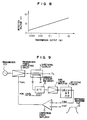
- FIG. 1 Hitherto, what is called at automatic power control (APC) circuit as shown in Fig. 1 has been known as such a kind of transmission output control circuit.
- APC automatic power control
- Such an APC circuit functions so as to keep a transmission output constant for fluctuations of various conditions such as power supply voltage, input, temperature, and the like.
- reference numeral 1 denotes a transmission VCO (Voltage Controlled Oscillator); 2 a transmission power amplifying circuit; 3 a directional coupler; 4 a detecting circuit using a diode; and 5 a comparison error amplifier.
- An output from the transmission VCO 1 is power amplified by the transmission power amplifying circuit 2 and is transmitted through the directional coupler 3.
- the directional coupler 3 branches a part of the output of the amplifying circuit 2 and supplies to the detecting circuit 4.
- a detected output of the detecting circuit 4 is supplied to the comparison error amplifier 5.
- the amplifier 5 compares the received detection output and a reference waveform 8 (V ref ) and gives a control voltage V APC to the amplifying circuit 2 in accordance with the result of the comparison, thereby controlling an amplification factor.
- V ref a reference waveform 8
- V APC control voltage
- a transmission output control negative feedback loop is constructed as-mentioned above.
- a transmission output level ordinarily has a discrete value.
- a difference between the maximum and minimum levels is up to 20 and a few dB. Therefore, an object of such a loop can be substantially accomplished by a simple detecting circuit using a diode which has generally been well known.
- the leading and trailing response time characteristics are set by specifying an output lower limit of -36 dBm or a point of a level relative ratio of -70 dBC to a peak value and a point of -30 dBC and a time which is requires to reach the peak value.
- the dynamic range is naturally narrow and the dynamic range is set to merely up to 20 at most and a few dB and it is considerable short of controllable transmission output ranges necessary for practical applications.
- a transmission output control circuit for a TDMA radio transmitter comprises: a directional coupler to separate a part of an output of a transmission power amplifying circuit; a variable attenuator to attenuate a separated output; a detecting circuit to detect an output of the variable attenuator; and means for controlling an amplification factor of the transmission power amplifying circuit in accordance with the result of the comparison between an output of the detecting circuit and a reference value.
- a transmission output control circuit for a TDMA radio transmitter comprises: a directional coupler to separate a part of an output of a transmission power amplifying circuit; a non-linear amplifier to non-linearly amplify a separated output; a detecting circuit to detect an output of the non-linear amplifier; and means for controlling an amplification factor of the transmission power amplifying circuit in accordance with the result of the comparison between an output of the detecting circuit and a reference value.
- a transmission output control circuit for a TDMA radio transmitter comprises: a directional coupler to separate a part of an output of a transmission power amplifying circuit; a variable attenuator to attenuate a separated output; a nonlinear amplifier to amplify an output of the variable attenuator in dependence upon logarithmic function; a detecting circuit to detect an output of the non-linear amplifier; and means for controlling an amplification factor of the transmission power amplifying circuit in accordance with the result of the comparison between an output of the detecting circuit and a reference value.
- a part of the transmission output generated from the transmission power amplifying circuit is taken out by the directional coupler and passes through the variable attenuator and is detected by the detecting circuit.
- the detected value decreases and the transmission output appears to decrease, whereby a control is made to increase the transmission output by the negative feedback loop. Accordingly, the transmission output can be controlled for an extended wide dynamic range with a high reproduction fidelity by the combination with the control by the variable attenuator without relying on an increase in the dynamic range of the detecting circuit.
- a part of the transmission output generated from the transmission power amplifying circuit is extracted by the directional coupler and is amplified by the non-linear amplifier in dependence upon a logarithmic function and is detected by the detecting circuit, so that the detection output which has been almost linearly corrected is derived. Consequently, the dynamic range of the detecting circuit is equivalently enlarged and the amplification factor of the transmission power amplifying circuit is controlled on the basis of the detection output.
- a part of the transmission output generated from the transmission power amplifying circuit is extracted by the directional coupler and passes through the variable attenuator and also passes through the non-linear amplifier and is detected by the detecting circuit.
- the detection value decreases and the transmission output appears to decrease, whereby a control is made to increase the transmission output by the negative feedback loop.
- the nonlinear amplifier operates to enlarge the dynamic range of the detecting characteristics.
- the transmission burst output can be relatively easily controlled for a wide dynamic range with a high precision by controlling in combination with the variable attenuator without relaying on only the extension in the dynamic range of the detecting circuit.
- Fig. 2 is a diagram showing the first embodiment of the invention.
- reference numeral 1 denotes the transmission VCO; 2 the transmission power amplifying circuit; 3 the directional coupler to extract a part of a transmission power; 4 the detecting circuit using a diode; and 5 the comparison error amplifier as a differential amplifier.
- Reference numeral 6 denotes a variable attenuating circuit for attenuating the transmission output extracted by the directional coupler 3 and for supplying to the detecting circuit 4.
- a control line is connected to the variable attenuating circuit 6, so that an arbitrary attenuation amount can be instantaneously derived.
- a switching control of an output level is mainly executed on the control line of the variable attenuating circuit 6.
- the transmission output ranges from 43 dBm to 13 dBm, which is divided into 16 steps with a span or difference of a 2 dB therebetween.
- a time mask of a burst waveform is specified by a relative value and the dynamic power control for 30 dB or more is needed.
- the control is executed from the level of -17 dBm or less, so that a control range is needed to cover a wide range of 60 dB.
- the dynamic range which is necessary for the control of the burst waveform is shared and provided by the detecting circuit and the control of the transmission power level of a high precision of a 2 dB step is shared and provided by the variable attenuator.
- Fig. 3 shows an example of such a construction.
- the variable attenuating circuit 6 comprises a 2 dB attenuating section 61, a 4 dB attenuating section 62, an 8 dB attenuating section 63, and a 16 dB attenuating section 64.
- the attenuation amount can be controlled to produce 16 attenuation variables stepped with an increment of 2 dB from 0 dB to 30 dB by transmission output level 4-bit data D1, D2, D3, and D4.
- one control line may be used by depending upon analog control or the attenuation amount may be controlled by a single attenuator through a D/A converter, it is necessary to secure a precision for the control of attenuation amount.
- the first embodiment enables the TDMA transmission output to be controlled by the construction as mentioned above.
- the output control of the dynamic range of 70 dB mentioned above is divided into the control of the burst waveform and the control of the output level.
- the control of the burst waveform is performed to prevent spread of the related frequency spectrum and such a control is executed by fully using the dynamic range of the detecting circuit 4 from the lower limit to the upper limit. It is generally sufficient to use a detecting range from 30 to 40 dB. Therefore, the reference waveform 8 which is supplied to the comparison error amplifier 5 is fundamentally constant irrespective of the transmission power level.
- an attenuation amount of the variable attenuating circuit 6 is set in accordance with the value of the transmission power level. That is, when the output is maximum, the attenuation amount is also maximum. To reduce the output, for instance, on a 2 dB unit basis (i.e., with every decrement of 2 dB), it is sufficient to also reduce the attenuation amount on a 2 dB unit basis (with every decrement of 2 dB). Namely, the change width of the variable attenuating circuit 6 coincides with the change width of the transmission output.
- variable attenuating circuit since a variation of the attenuating characteristic can be more easily managed than a variation of the detecting characteristic, a precision of the output level rises.
- a practical method of constructing the variable attenuating circuit it is also possible to make a device to raise the precision by mixedly arranging or disposing linear amplifiers in order to improve the impedance characteristic and the isolation characteristic.
- the control of the wide transmission output control is shared by the variable attenuator which can be digitally controlled and the diode detecting circuit of high reproducibility. Therefore, the output control having a high precision and an excellent reproducing fidelity can be accomplished as compared with the conventional transmission output control circuit which depends on only the dynamic range of the detecting circuit.
- Fig. 4 is a diagram showing the second embodiment of the invention.
- Reference numeral 7 denotes a non-linear amplifier such as RF frequency logarithm amplifier or saturation type amplifier whose input and output characteristics are relatively similar to those of the logarithm amplifier.
- a part of the transmission power which has been amplified by the transmission power amplifying circuit 2 is extracted by the directional coupler 3 and is supplied to the non-linear amplifier 7.
- An amplifier whose amplifying characteristic changes in a logarithmic function manner as shown in Fig. 5 is used as a non-linear amplifier 7.
- the non-linear amplifier having such a characteristic can be realized by a saturation type amplifier by an RF amplifier using two transistors as shown in Fig. 6. An output of the non-linear amplifier 7 is supplied to the detecting circuit 4. If a diode detecting circuit is used as a detecting circuit 4, the detecting circuit has a detecting characteristic such that a detection voltage suddenly rises with an increase in input signal level as shown in Fig. 7. A synthetic characteristic with the characteristic of the non-linear amplifier 7, therefore, is as shown in a linear characteristic of Fig. 8.
- the second embodiment intends to widen the dynamic range of the detecting circuit 4 by the construction as mentioned above.
- the detecting characteristic of the diode is as shown in Fig. 7 and the detected voltage suddenly rises with an increase in input signal level.
- a detecting sensitivity is also not constant and a control loop gain also decreases when the input signal level is small.
- the non-linear amplifier 7 Since the non-linear amplifier 7 has the characteristics such that the gain decreases with an increase in input signal level as shown in Fig. 5, by arranging the non-linear amplifier 7 at a front stage of the detecting circuit 4, the dynamic range of the detecting characteristic can be enlarged as shown in Fig. 8.
- the invention is not limited to the amplifier having the strict logarithm converting characteristics. However, the above object is not accomplished by the linear amplifier. On the other hand, when a phase delay between the input and the output is large, such a case is improper to the high speed burst control as an object of the invention.
- the waveform of the transmission burst wave can be controlled by using the fairly enlarged detecting characteristic and the transmission output changes at a high speed in accordance with the reference waveform 8 which is supplied to the comparison error amplifier 5.
- the non-linear amplifier at the front stage of the detecting circuit, there are advantages such that the dynamic range of the transmission output detecting circuit can be fairly increased and the output control of the burst-shaped transmission wave can be performed.
- Fig. 9 is a diagram showing a construction of the third embodiment of the invention.
- the same parts and components as those shown in Figs. 2 and 4 are designated by the same reference numerals and their descriptions are omitted here.
- a non-linear amplifier using a logarithm amplifier or a saturation type amplifier is arranged before the diode detecting circuit 4.
- Fig. 5 shows input and output characteristics of the third embodiment. It is sufficient to reduce the gain with an increase in input signal level and the invention is not particularly limited to the amplifier having the strict logarithm converting characteristics.
- variable attenuating circuit 6 The control of the transmission level which requires a precision of a 2 dB step (i.e., 2 dB stepped control of the level) is executed by the variable attenuating circuit 6.
- variable attenuating circuit 6 and the non-linear amplifier 7 have been connected and arranged at the front stage of the diode detecting circuit 4 in the third embodiment, the wide transmission output control range has respectively been assigned to the variable attenuating circuit 6 which can be digitally controlled and the detecting circuit 4 in which the non-linear amplifier 7 such as logarithm amplifier or saturation type amplifier has been arranged at the front stage and the dynamic range of the detecting characteristic has been enlarged. Consequently, the control of the transmission burst wave which could not be performed by the conventional transmission output control circuit which depends on only the dynamic range of the diode detecting circuit can be realized at a high precision and a high reproducing fidelity.
- the third embodiment enables the TDMA transmission output control to be performed by the construction as mentioned above.
- the output control of the dynamic range of 70 dB mentioned above is separated into the control of the burst waveform and the control of the output level.
- the control of the burst waveform is executed to prevent a spread of the frequency spectrum and ordinarily needs the dynamic range of the detection within a range from 30 to 40 dB.
- the dynamic range is set to about 20 dB. If the saturation type amplifier having the input and output characteristics as shown in Fig.
- the amplification gain is high at a low level and the detection lower limit is extended by only such a gain, while the gain gradually decreases at a high level, so that a sudden increase in detection voltage is suppressed and the detecting characteristics are as shown in Fig. 8.
- the waveform of the transmission burst wave can be controlled and the reference input waveform 8 which is supplied to the comparison error amplifier becomes constant irrespective of the transmission power level as will be explained hereinlater.
- an attenuation amount of the variable attenuating circuit 6 is set in accordance with such a value for the control of the transmission power level. That is, the attenuation amount is also maximum when the output is maximum. To decrease the output, for example, on a 2 dB step unit basis, it is sufficient to also reduce the attenuation amount on a 2 dB unit basis.
- the change amount of the attenuation amount coincides with the change amount of the transmission output.
- the setting precision of the output level rises upon manufacturing.
- the invention is not limited to the construction using only the attenuators but can also use a construction in which linear amplifying circuits are mixedly arranged, thereby improving the impedance and isolation characteristics and raising the precision.
Landscapes
- Transmitters (AREA)
- Control Of Amplification And Gain Control (AREA)
Applications Claiming Priority (6)
| Application Number | Priority Date | Filing Date | Title |
|---|---|---|---|
| JP219217/90 | 1990-08-20 | ||
| JP2219215A JPH0771054B2 (ja) | 1990-08-20 | 1990-08-20 | 送信出力制御回路 |
| JP219216/90 | 1990-08-20 | ||
| JP21921790A JPH0783327B2 (ja) | 1990-08-20 | 1990-08-20 | 送信出力制御回路 |
| JP219215/90 | 1990-08-20 | ||
| JP2219216A JPH0783326B2 (ja) | 1990-08-20 | 1990-08-20 | 送信出力制御回路 |
Publications (3)
| Publication Number | Publication Date |
|---|---|
| EP0472330A2 true EP0472330A2 (fr) | 1992-02-26 |
| EP0472330A3 EP0472330A3 (en) | 1992-05-20 |
| EP0472330B1 EP0472330B1 (fr) | 1995-10-18 |
Family
ID=27330253
Family Applications (1)
| Application Number | Title | Priority Date | Filing Date |
|---|---|---|---|
| EP91307314A Expired - Lifetime EP0472330B1 (fr) | 1990-08-20 | 1991-08-08 | Circuit de commande de niveau d'émission |
Country Status (4)
| Country | Link |
|---|---|
| US (1) | US5214393A (fr) |
| EP (1) | EP0472330B1 (fr) |
| DE (1) | DE69113925T2 (fr) |
| FI (1) | FI104299B1 (fr) |
Cited By (12)
| Publication number | Priority date | Publication date | Assignee | Title |
|---|---|---|---|---|
| EP0546693A1 (fr) * | 1991-11-29 | 1993-06-16 | Matsushita Electric Industrial Co., Ltd. | Méthode de contrôle et circuit de contrôle pour un transmetteur |
| FR2690021A1 (fr) * | 1992-04-14 | 1993-10-15 | Alcatel Telspace | Amplificateur hyperfréquence comportant une boucle de régulation à très grande dynamique. |
| EP0566406A1 (fr) * | 1992-04-17 | 1993-10-20 | Hughes Aircraft Company | Méthode de commande automatique de la puissance de sortie d'un amplificateur |
| WO1994001929A1 (fr) * | 1992-07-01 | 1994-01-20 | At&T Wireless Communications Products Ltd. | Procede et appareil de regulation de la puissance de sortie d'un amplificateur |
| EP0573073A3 (fr) * | 1992-06-05 | 1994-02-23 | Japan Radio Co Ltd | |
| EP0509733A3 (en) * | 1991-04-16 | 1994-05-11 | Mitsubishi Electric Corp | Radio-frequency power amplifier device |
| US5434537A (en) * | 1993-02-12 | 1995-07-18 | Nokia Mobile Phones Ltd. | Circuit for measuring the output power from an amplifier |
| RU2124809C1 (ru) * | 1996-08-05 | 1999-01-10 | Самсунг Электроникс Ко., Лтд. | Устройство и способ отслеживания мощности передачи с использованием сообщения о рабочей нагрузке |
| WO2000048311A1 (fr) * | 1999-02-11 | 2000-08-17 | Siemens Aktiengesellschaft | Procede et dispositif pour reguler la puissance d'un amplificateur d'emission |
| RU2158481C2 (ru) * | 1994-07-21 | 2000-10-27 | Квэлкомм Инкорпорейтед | Способ и устройство для балансировки границы передачи связи в прямой линии связи с границей передачи связи в обратной линии связи в системе сотовой связи |
| WO2002095931A3 (fr) * | 2001-05-22 | 2004-02-12 | Analog Devices Inc | Module amplificateur de puissance calibre |
| WO2011095214A1 (fr) * | 2010-02-04 | 2011-08-11 | Epcos Ag | Circuit amplificateur et procédé de détection de signal |
Families Citing this family (34)
| Publication number | Priority date | Publication date | Assignee | Title |
|---|---|---|---|---|
| JP2776071B2 (ja) * | 1991-07-19 | 1998-07-16 | 松下電器産業株式会社 | 送信出力包絡線検波回路および線形送信回路 |
| CA2088813C (fr) * | 1992-03-02 | 2004-02-03 | Willem G. Durtler | Circuit de commande automatique de niveau pour radiotelephone a modes analogique et numerique |
| JPH06260864A (ja) * | 1993-03-08 | 1994-09-16 | Matsushita Electric Ind Co Ltd | 送信出力増幅器 |
| FI97177C (fi) * | 1993-09-06 | 1996-10-25 | Nokia Telecommunications Oy | Menetelmä ja järjestely suurtaajuustehovahvistimen toiminnan ohjaamiseen |
| US5423081A (en) * | 1993-08-16 | 1995-06-06 | Hughes Aircraft Company | Cellular power amplifier power level control circuitry |
| GB9320078D0 (en) * | 1993-09-29 | 1993-11-17 | Linear Modulation Tech | Cartesian amplifier power control and related applications |
| JP2861749B2 (ja) * | 1993-09-30 | 1999-02-24 | 日本電気株式会社 | 出力レベル制御回路 |
| KR960009446B1 (en) * | 1993-12-23 | 1996-07-19 | Hyundai Electronics Ind | A diversity device of gps antenna |
| US5640691A (en) * | 1994-12-19 | 1997-06-17 | Lucent Technologies Inc. | Power controller for RF transmitters |
| FI101505B1 (fi) * | 1995-05-10 | 1998-06-30 | Nokia Mobile Phones Ltd | Menetelmä suuntakytkimellä toteutetun tehonmittauksen parantamiseksi pienillä tehotasoilla |
| US5724003A (en) * | 1995-12-29 | 1998-03-03 | Maxim Integrated Products, Inc. | Methods and apparatus for signal amplitude control systems |
| JPH09205333A (ja) * | 1996-01-24 | 1997-08-05 | Sony Corp | 電力増幅回路 |
| US6233438B1 (en) * | 1998-03-26 | 2001-05-15 | Ericsson Inc. | Wide-range power control systems and methods for radio frequency transmitters and mobile radiotelephones |
| JP3712160B2 (ja) * | 1998-04-17 | 2005-11-02 | 松下電器産業株式会社 | 無線装置、無線装置における送信電力制御方法および記録媒体 |
| US6466772B1 (en) * | 1998-09-25 | 2002-10-15 | Skyworks Solutions, Inc. | Apparatus and method for improving power control loop linearity |
| JP3169002B2 (ja) * | 1998-12-18 | 2001-05-21 | 日本電気株式会社 | 送信出力制御回路 |
| US6377784B2 (en) * | 1999-02-09 | 2002-04-23 | Tropian, Inc. | High-efficiency modulation RF amplifier |
| US6321074B1 (en) * | 1999-02-18 | 2001-11-20 | Itron, Inc. | Apparatus and method for reducing oscillator frequency pulling during AM modulation |
| US6370364B1 (en) * | 1999-06-22 | 2002-04-09 | Nokia Mobile Phones, Ltd. | Mobile station having power control loop offset alignment without requiring RF power measurement |
| JP2001016116A (ja) | 1999-07-02 | 2001-01-19 | Nec Corp | 携帯無線機 |
| EP1277273B1 (fr) * | 2000-03-03 | 2007-01-24 | Siemens Aktiengesellschaft | Procede et circuit d'emission pour creer un signal d'emission |
| US6920334B1 (en) | 2000-03-24 | 2005-07-19 | International Business Machines Corporation | Method and apparatus for providing gain control feedback in RF amplifiers |
| US6711392B1 (en) * | 2000-06-30 | 2004-03-23 | International Business Machines Corporation | Balanced power amplifier for low power radio communications |
| FR2813487B1 (fr) * | 2000-08-31 | 2002-11-29 | Cit Alcatel | Procede et dispositif de controle de l'amplification du signal emis par un terminal mobile permettant d'augmenter l'autonomie dudit terminal mobile |
| US7471935B2 (en) * | 2000-10-23 | 2008-12-30 | Intel Corporation | Automatic level control |
| GB2368737B (en) * | 2000-10-31 | 2004-11-10 | Roke Manor Research | Method and apparatus for controlling an amplifier |
| US6404284B1 (en) | 2001-04-19 | 2002-06-11 | Anadigics, Inc. | Amplifier bias adjustment circuit to maintain high-output third-order intermodulation distortion performance |
| US6934520B2 (en) * | 2002-02-21 | 2005-08-23 | Semiconductor Components Industries, L.L.C. | CMOS current mode RF detector and method |
| US20040198261A1 (en) * | 2002-06-28 | 2004-10-07 | Wei Xiong | Method of self-calibration in a wireless transmitter |
| US6836187B2 (en) * | 2002-09-23 | 2004-12-28 | Agilent Technologies, Inc | RF peak-to-peak detector with wide dynamic range |
| US7236745B2 (en) * | 2003-03-05 | 2007-06-26 | Harris Stratex Networks Operating Corporation | Transceiver power detection architecture |
| US7228114B2 (en) * | 2003-05-21 | 2007-06-05 | Harris Stratex Networks Operating Corporation | Wide dynamic range power detection scheme |
| JP4244907B2 (ja) * | 2004-10-25 | 2009-03-25 | ソニー株式会社 | 光ディスク装置 |
| US7164285B1 (en) | 2005-08-12 | 2007-01-16 | Stratex Networks, Inc. | Directional power detection by quadrature sampling |
Family Cites Families (7)
| Publication number | Priority date | Publication date | Assignee | Title |
|---|---|---|---|---|
| JPS6110327Y2 (fr) * | 1980-01-10 | 1986-04-03 | ||
| JPS57154919A (en) * | 1981-03-20 | 1982-09-24 | Hitachi Denshi Ltd | Detecting system for high frequency faulty power level |
| US4523155A (en) * | 1983-05-04 | 1985-06-11 | Motorola, Inc. | Temperature compensated automatic output control circuitry for RF signal power amplifiers with wide dynamic range |
| JPS6041821A (ja) * | 1983-08-18 | 1985-03-05 | Nec Corp | 送信出力電力制御装置 |
| US4602218A (en) * | 1985-04-30 | 1986-07-22 | Motorola, Inc. | Automatic output control circuitry for RF power amplifiers with wide dynamic range |
| JPH0630031B2 (ja) * | 1986-09-25 | 1994-04-20 | 日本電気株式会社 | 自動電力制御回路 |
| US5126686A (en) * | 1989-08-15 | 1992-06-30 | Astec International, Ltd. | RF amplifier system having multiple selectable power output levels |
-
1991
- 1991-08-06 US US07/740,966 patent/US5214393A/en not_active Expired - Lifetime
- 1991-08-08 DE DE69113925T patent/DE69113925T2/de not_active Expired - Fee Related
- 1991-08-08 EP EP91307314A patent/EP0472330B1/fr not_active Expired - Lifetime
- 1991-08-20 FI FI913935A patent/FI104299B1/fi not_active IP Right Cessation
Cited By (17)
| Publication number | Priority date | Publication date | Assignee | Title |
|---|---|---|---|---|
| EP0509733A3 (en) * | 1991-04-16 | 1994-05-11 | Mitsubishi Electric Corp | Radio-frequency power amplifier device |
| US5376895A (en) * | 1991-11-29 | 1994-12-27 | Matsushita Electric Industrial Co., Ltd. | Control circuit and method for transmission output |
| EP0546693A1 (fr) * | 1991-11-29 | 1993-06-16 | Matsushita Electric Industrial Co., Ltd. | Méthode de contrôle et circuit de contrôle pour un transmetteur |
| FR2690021A1 (fr) * | 1992-04-14 | 1993-10-15 | Alcatel Telspace | Amplificateur hyperfréquence comportant une boucle de régulation à très grande dynamique. |
| EP0566406A1 (fr) * | 1992-04-17 | 1993-10-20 | Hughes Aircraft Company | Méthode de commande automatique de la puissance de sortie d'un amplificateur |
| EP0573073A3 (fr) * | 1992-06-05 | 1994-02-23 | Japan Radio Co Ltd | |
| US5383223A (en) * | 1992-06-05 | 1995-01-17 | Japan Radio Co., Ltd. | Power control device wherein a bias voltage in level detection is given a constant difference from a detected voltage |
| US5483198A (en) * | 1992-07-01 | 1996-01-09 | At&T Wireless Communications Products, Ltd. | Method and apparatus for controlling amplifier power |
| WO1994001929A1 (fr) * | 1992-07-01 | 1994-01-20 | At&T Wireless Communications Products Ltd. | Procede et appareil de regulation de la puissance de sortie d'un amplificateur |
| US5434537A (en) * | 1993-02-12 | 1995-07-18 | Nokia Mobile Phones Ltd. | Circuit for measuring the output power from an amplifier |
| RU2158481C2 (ru) * | 1994-07-21 | 2000-10-27 | Квэлкомм Инкорпорейтед | Способ и устройство для балансировки границы передачи связи в прямой линии связи с границей передачи связи в обратной линии связи в системе сотовой связи |
| RU2124809C1 (ru) * | 1996-08-05 | 1999-01-10 | Самсунг Электроникс Ко., Лтд. | Устройство и способ отслеживания мощности передачи с использованием сообщения о рабочей нагрузке |
| WO2000048311A1 (fr) * | 1999-02-11 | 2000-08-17 | Siemens Aktiengesellschaft | Procede et dispositif pour reguler la puissance d'un amplificateur d'emission |
| US6426675B1 (en) | 1999-02-11 | 2002-07-30 | Siemens Aktiengesellschaft | Method and arrangement for controlling the power of a transmission amplifier |
| WO2002095931A3 (fr) * | 2001-05-22 | 2004-02-12 | Analog Devices Inc | Module amplificateur de puissance calibre |
| WO2011095214A1 (fr) * | 2010-02-04 | 2011-08-11 | Epcos Ag | Circuit amplificateur et procédé de détection de signal |
| US8629719B2 (en) | 2010-02-04 | 2014-01-14 | Epcos Ag | Amplifier circuit and method for signal sensing |
Also Published As
| Publication number | Publication date |
|---|---|
| DE69113925D1 (de) | 1995-11-23 |
| FI104299B (fi) | 1999-12-15 |
| US5214393A (en) | 1993-05-25 |
| FI913935A0 (fi) | 1991-08-20 |
| FI913935L (fi) | 1992-02-21 |
| EP0472330B1 (fr) | 1995-10-18 |
| DE69113925T2 (de) | 1996-05-30 |
| EP0472330A3 (en) | 1992-05-20 |
| FI104299B1 (fi) | 1999-12-15 |
Similar Documents
| Publication | Publication Date | Title |
|---|---|---|
| EP0472330B1 (fr) | Circuit de commande de niveau d'émission | |
| US4602218A (en) | Automatic output control circuitry for RF power amplifiers with wide dynamic range | |
| US4523155A (en) | Temperature compensated automatic output control circuitry for RF signal power amplifiers with wide dynamic range | |
| CA2088813C (fr) | Circuit de commande automatique de niveau pour radiotelephone a modes analogique et numerique | |
| US5307512A (en) | Power control circuitry for achieving wide dynamic range in a transmitter | |
| US5376895A (en) | Control circuit and method for transmission output | |
| US6166598A (en) | Power amplifying circuit with supply adjust to control adjacent and alternate channel power | |
| US5107487A (en) | Power control of a direct sequence CDMA radio | |
| EP0786859A2 (fr) | Amplificateur de puissance et procédé de contrÔle de puissance | |
| US5915213A (en) | Transmitter apparatus with linearizing circuit to compensate for distortion in power amplifier | |
| JP2005518684A (ja) | 電力増幅器の制御 | |
| GB2317283A (en) | Transmitter with power control in both if and rf sections | |
| KR101050928B1 (ko) | 무선 통신 장치의 qam 송신기 유닛을 위한 자동 전력제어 회로 | |
| US5697073A (en) | Apparatus and method for shaping and power controlling a signal in a transmitter | |
| US5912588A (en) | Gain control circuit for a linear power amplifier | |
| EP1568236B1 (fr) | Amplificateur de commande radiofrequence a gain variable en continu comportant des caracteristiques de controle de gain lineaire en decibels | |
| WO2003075452A2 (fr) | Procede de reglage du gain et de la consommation de courant dans un circuit amplificateur de puissance avec conservation de la linearite | |
| US5309115A (en) | Burst control circuit for use in TDMA communications system | |
| CA2087744A1 (fr) | Dispositif de commande pour amplificateur de puissance | |
| JPH0771054B2 (ja) | 送信出力制御回路 | |
| JPH0783326B2 (ja) | 送信出力制御回路 | |
| US6091299A (en) | Method and apparatus for achieving linearized response of PIN diode attenuators | |
| JPH08288772A (ja) | 送信電力増幅器のバイアス制御回路 | |
| JPH05129860A (ja) | 電力増幅装置及び送信装置 | |
| JPH06152288A (ja) | 電力制御装置 |
Legal Events
| Date | Code | Title | Description |
|---|---|---|---|
| PUAI | Public reference made under article 153(3) epc to a published international application that has entered the european phase |
Free format text: ORIGINAL CODE: 0009012 |
|
| AK | Designated contracting states |
Kind code of ref document: A2 Designated state(s): DE FR GB SE |
|
| PUAL | Search report despatched |
Free format text: ORIGINAL CODE: 0009013 |
|
| AK | Designated contracting states |
Kind code of ref document: A3 Designated state(s): DE FR GB SE |
|
| 17P | Request for examination filed |
Effective date: 19920609 |
|
| 17Q | First examination report despatched |
Effective date: 19931022 |
|
| GRAA | (expected) grant |
Free format text: ORIGINAL CODE: 0009210 |
|
| AK | Designated contracting states |
Kind code of ref document: B1 Designated state(s): DE FR GB SE |
|
| REF | Corresponds to: |
Ref document number: 69113925 Country of ref document: DE Date of ref document: 19951123 |
|
| ET | Fr: translation filed | ||
| PGFP | Annual fee paid to national office [announced via postgrant information from national office to epo] |
Ref country code: SE Payment date: 19960610 Year of fee payment: 6 |
|
| PGFP | Annual fee paid to national office [announced via postgrant information from national office to epo] |
Ref country code: GB Payment date: 19960725 Year of fee payment: 6 |
|
| PLBE | No opposition filed within time limit |
Free format text: ORIGINAL CODE: 0009261 |
|
| STAA | Information on the status of an ep patent application or granted ep patent |
Free format text: STATUS: NO OPPOSITION FILED WITHIN TIME LIMIT |
|
| PGFP | Annual fee paid to national office [announced via postgrant information from national office to epo] |
Ref country code: FR Payment date: 19960828 Year of fee payment: 6 |
|
| 26N | No opposition filed | ||
| PGFP | Annual fee paid to national office [announced via postgrant information from national office to epo] |
Ref country code: DE Payment date: 19961031 Year of fee payment: 6 |
|
| PG25 | Lapsed in a contracting state [announced via postgrant information from national office to epo] |
Ref country code: GB Free format text: LAPSE BECAUSE OF NON-PAYMENT OF DUE FEES Effective date: 19970808 |
|
| PG25 | Lapsed in a contracting state [announced via postgrant information from national office to epo] |
Ref country code: SE Free format text: LAPSE BECAUSE OF NON-PAYMENT OF DUE FEES Effective date: 19970809 |
|
| GBPC | Gb: european patent ceased through non-payment of renewal fee |
Effective date: 19970808 |
|
| PG25 | Lapsed in a contracting state [announced via postgrant information from national office to epo] |
Ref country code: FR Free format text: LAPSE BECAUSE OF NON-PAYMENT OF DUE FEES Effective date: 19980430 |
|
| PG25 | Lapsed in a contracting state [announced via postgrant information from national office to epo] |
Ref country code: DE Free format text: LAPSE BECAUSE OF NON-PAYMENT OF DUE FEES Effective date: 19980501 |
|
| EUG | Se: european patent has lapsed |
Ref document number: 91307314.4 |
|
| REG | Reference to a national code |
Ref country code: FR Ref legal event code: ST |