EP0472938A2 - Dispositif pour tester et réparer un circuit intégré - Google Patents
Dispositif pour tester et réparer un circuit intégré Download PDFInfo
- Publication number
- EP0472938A2 EP0472938A2 EP91112862A EP91112862A EP0472938A2 EP 0472938 A2 EP0472938 A2 EP 0472938A2 EP 91112862 A EP91112862 A EP 91112862A EP 91112862 A EP91112862 A EP 91112862A EP 0472938 A2 EP0472938 A2 EP 0472938A2
- Authority
- EP
- European Patent Office
- Prior art keywords
- integrated circuit
- ion beam
- testing
- signal
- electrode
- Prior art date
- Legal status (The legal status is an assumption and is not a legal conclusion. Google has not performed a legal analysis and makes no representation as to the accuracy of the status listed.)
- Granted
Links
Images

Classifications
-
- H—ELECTRICITY
- H10—SEMICONDUCTOR DEVICES; ELECTRIC SOLID-STATE DEVICES NOT OTHERWISE PROVIDED FOR
- H10P—GENERIC PROCESSES OR APPARATUS FOR THE MANUFACTURE OR TREATMENT OF DEVICES COVERED BY CLASS H10
- H10P74/00—Testing or measuring during manufacture or treatment of wafers, substrates or devices
- H10P74/23—Testing or measuring during manufacture or treatment of wafers, substrates or devices characterised by multiple measurements, corrections, marking or sorting processes
- H10P74/232—Testing or measuring during manufacture or treatment of wafers, substrates or devices characterised by multiple measurements, corrections, marking or sorting processes comprising connection or disconnection of parts of a device in response to a measurement
-
- G—PHYSICS
- G01—MEASURING; TESTING
- G01R—MEASURING ELECTRIC VARIABLES; MEASURING MAGNETIC VARIABLES
- G01R31/00—Arrangements for testing electric properties; Arrangements for locating electric faults; Arrangements for electrical testing characterised by what is being tested not provided for elsewhere
- G01R31/28—Testing of electronic circuits, e.g. by signal tracer
- G01R31/302—Contactless testing
-
- H—ELECTRICITY
- H10—SEMICONDUCTOR DEVICES; ELECTRIC SOLID-STATE DEVICES NOT OTHERWISE PROVIDED FOR
- H10W—GENERIC PACKAGES, INTERCONNECTIONS, CONNECTORS OR OTHER CONSTRUCTIONAL DETAILS OF DEVICES COVERED BY CLASS H10
- H10W20/00—Interconnections in chips, wafers or substrates
- H10W20/40—Interconnections external to wafers or substrates, e.g. back-end-of-line [BEOL] metallisations or vias connecting to gate electrodes
- H10W20/49—Adaptable interconnections, e.g. fuses or antifuses
- H10W20/493—Fuses, i.e. interconnections changeable from conductive to non-conductive
- H10W20/494—Fuses, i.e. interconnections changeable from conductive to non-conductive changeable by the use of an external beam, e.g. laser beam or ion beam
Definitions
- the invention relates to a method according to the preamble of claim 1 and an arrangement according to the preamble of claim 4 for testing and repairing an integrated circuit.
- the invention is therefore based on the object of developing the method according to the preamble of claim 1 and the arrangement according to the preamble of claim 4 in such a way that the time and cost involved in testing and repairing an integrated circuit are significant compared to the prior art is lowered.
- the ion beam used for the repair also forms the corpuscular beam used for the test process and a single beam generating device is provided for generating this beam.
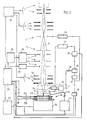
- the exemplary embodiment of an arrangement for testing and repairing an integrated circuit shown in FIG. 1 contains an ion source 1, a condenser lens 2, a blanking system 3, an aperture stop 4, a deflection device 5, a stigmator 6 and an objective lens 7.
- the objective lens 7 contains three Arranged one behind the other in the beam direction, rotationally symmetrical electrodes 7a, 7b, 7c, the axis 8 of the ion beam coinciding with the axis of the objective lens 7.
- a secondary electron spectrometer is also integrated, which essentially contains an extraction electrode 9, a filter electrode 10, a secondary electron detector 11 and a control circuit to be explained in more detail.
- the secondary electron detector 11 essentially consists of a scintillator 12, which is formed by the inner region of the central electrode 7b of the objective lens 7, a mirror 13 (or other optics) and a multiplier 14. Instead, the scintillator 12 can also be used an optical fiber can be connected to the multiplier 14.
- the device for applying an input signal to an integrated circuit 23 is formed by an LSI tester 22, which is connected to the integrated circuit 23 via a test head 15.
- the control circuit which connects the scintillator 12 to the filter electrode 10, contains the LSI tester 22 with test head 15, a phase controller 16, a delay device 17, a gate controller 18, a preamplifier 19, a signal processing circuit 20 and an amplifier 21, the output of which is connected to the filter electrode 10.
- the output of the phase control 16 connected to the delay device 17 is also connected to the blanking system 3 via a pulse generator 22.
- a data processing system 25 controls the LSI tester 22 and the phase controller 16. A corresponding return signal is led from the signal processing circuit 20 to the data processing system 25.
- the integrated circuit 23 to be examined is located on a table 26 which can be displaced in any direction perpendicular to the axis of the objective lens 7.
- the shift is done by two motors 27a, 27b controlled by the data processing system 25 via a control unit 28.
- a driver 29 is provided for actuating the deflection device 5 and is driven by the data processing system 25 via a control 30.
- the stigmator 6 is also connected to the data processing system 25 via a controller 31.
- Another controller 32 connected to the data processing system 25 controls the ion source 1, the condenser lens 2 and the objective lens 7.
- a separation device 33 is provided with a nozzle 34, which is also controlled via the data processing system 25.
- the general principle of the control loop is to regulate the secondary electron signal to a constant current and at the same time to generate the phase control for the blanking system 3 of the ion beam.
- the secondary electrons 35 triggered by the ion beam when it hits the sample 23 must first pass through the filter electrode 10 after passing through the extraction electrode 9. Since the filter electrode is at a certain negative potential (which - as will be explained - is controlled by the control loop), only the secondary electrons which have a sufficiently high energy are let through through the filter electrode 10.
- the potential at the examined measuring point of the integrated circuit 23 changes, the energy distribution of the secondary electrons shifts and accordingly more or fewer electrons come to the scintillator 12 of the secondary electron detector 11. Now the potential of the filter electrode 10 is readjusted so that the secondary electron current remains constant . The potential of the filter electrode 10 is thus changed depending on the potential to be measured on the integrated circuit 23. The changing potential of the filter electrode 10 thus represents a measure of the potential of the integrated circuit 23 to be measured.
- the outer control circuit works as follows:
- the secondary electron detector 11 converts the secondary electrons generated by the ion beam at the measuring point - provided they pass through the filter electrode 10 - into an electrical actual signal which is scanned by the gate control 18 after amplification in the preamplifier 19 .
- This scanning is controlled by the LSI tester 22, which at the same time also drives the integrated circuit 23 to be examined via the test head 15.
- the phase controller 16 enables the sampling time to be set.
- the blanking system 3 of the ion beam is controlled from the output of the phase control 16 via the pulse generator 24.
- the delay device 17 is provided.
- the device for comparing the converted actual signal with the desired signal is formed by the signal processing circuit 20.
- the output signal of the preamplifier 19 sampled via the gate control 18 can be averaged in order to improve the signal-to-noise ratio.
- a comparator is used to carry out a comparison with the target signal, which corresponds to the desired constant secondary electron current.
- the output signal reaches the filter electrode 10 via the amplifier 21 and, in the manner already explained, keeps the secondary electron current constant by changing the negative potential of the filter electrode 10, even if the potential to be measured changes at the measuring point of the integrated circuit 23 under investigation.
- a pulsed ion source can of course also be used within the scope of the invention.
- the ion beam can be adjusted to any measuring point of the integrated circuit 23 by moving the table 26 by means of the motors 27a, 27b via the control unit 28.
- the relative movement of the ion beam and the integrated circuit 23 can also be solved within the scope of the invention by, for example, shifting the axis 8 of the ion beam and thus the entire apparatus perpendicular to the integrated circuit 23.
- An input signal is applied to the integrated circuit 23 by the LSI tester 22 via the test head 15, and the resulting output signal is in turn passed on to the LSI tester 22 via the test head 15. In this way, the information is obtained as to whether there is an error in the circuit. If there is an error, 22 different test programs are generated by the LSI tester in order to limit the error.
- Measuring points are defined by means of a CAD system and the electrical description of the integrated circuit 23. The individual measuring points are approached by the ion beam in order to carry out potential measurements there in the manner described above.
- the data processing system 25 receives from the signal processing circuit 20 at each measuring point the information as to whether there is a deviation of the actual signal from the target signal. These measurements are carried out repeatedly at various measuring points until the fault is precisely localized. The choice of the individual measuring points expediently depends on the results of the previous measurements. This can be done either automatically by the data processing system 25 or by the operator.
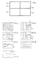
- FIGS. 4a to 4h show possible menus which can be combined in any way on the screen 36.
- FIG. 4 a shows a so-called SEM image of a section of the integrated circuit 23, which was created by scanning the integrated circuit with the ion beam.
- the reference point 37 denotes the measuring point to be examined.
- 4b shows the corresponding CAD layout over the same section of the integrated circuit 23, the position 38 corresponding to the measuring point 37 being shown from the layout.
- 4c illustrates a CAD block diagram, the measuring point 37 or the position 38 being designated by the corresponding position 39 in the block diagram.
- the waveform 40 in FIG. 4d corresponds, for example, to the waveform signal measured at the measuring point 37.
- the waveform 40 was created by simulation so that the operator can determine on the screen whether there are deviations between the measured and simulated waveform.
- the arrangement for testing and repairing an integrated circuit can also be used to carry out the repair immediately, without the integrated circuit 23 having to be implemented.
- the device for repairing an integrated circuit provided in this arrangement also uses an ion beam.
- the ion beam used for the repair also forms the ion beam used for the test process. This beam is generated in a single beam generating device, namely the ion source 1.
- conductor tracks can be cut with the ion beam, and on the other hand, conductive material can be applied to the integrated circuit by a separating device, so that new line connections are created.
- FIG. 4f A CAD layout is shown in FIG. 4f, the locations of the deposition 42 and the separation 43 being indicated.
- FIG. 4g the conductor track 44 and the cut 45 can be observed in a CAD layout.
- the separation process takes place by controlling the separation device 33 via the data processing system 25, the outlet opening of the nozzle 34 being brought into the correct position by moving the table 26.
- 4h shows a control menu in which the waveform signals generated by simulation and / or measurements can be compiled.
- the data processing system 25 has all circuit data of the integrated circuit 23, such as block diagrams, layout and mask data.
- the new integrated circuit created by a repair can in turn be stored in the data processing system and new simulations can be carried out for this circuit.
- the Time for a circuit development can be significantly reduced in this way.
- the arrangement for testing and repairing can therefore not only be used for finished integrated circuits - which are only to be checked again - but can also be used for the circuit construction in the development phase.
- the scintillator 12 is formed by the central electrode 7b of the objective lens 7.
- the scintillator 12 ' is arranged outside the objective lens 7.
- the secondary electron spectrometer contains a pressure electrode 46 and a deflection electrode 47.
- the pressure electrode 46 and the deflection electrode 47 ensure that the secondary electrons generated after passing through the filter electrode 10 reach the scintillator 12 'arranged on the side next to the secondary electron spectrometer. Otherwise, the structure and mode of operation are analogous to the exemplary embodiment according to FIG. 1.
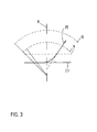
- the extraction electrode 9 and the filter electrode 10 are shown in FIG. 2 as planar networks, but can advantageously also be designed as spherical networks, as shown in FIG.
Landscapes
- Engineering & Computer Science (AREA)
- General Engineering & Computer Science (AREA)
- Physics & Mathematics (AREA)
- General Physics & Mathematics (AREA)
- Testing Or Measuring Of Semiconductors Or The Like (AREA)
- Tests Of Electronic Circuits (AREA)
- Testing Of Individual Semiconductor Devices (AREA)
- Design And Manufacture Of Integrated Circuits (AREA)
Applications Claiming Priority (2)
| Application Number | Priority Date | Filing Date | Title |
|---|---|---|---|
| DE4027062A DE4027062A1 (de) | 1990-08-27 | 1990-08-27 | Verfahren und anordnung zum testen und reparieren einer integrierten schaltung |
| DE4027062 | 1990-08-27 |
Publications (3)
| Publication Number | Publication Date |
|---|---|
| EP0472938A2 true EP0472938A2 (fr) | 1992-03-04 |
| EP0472938A3 EP0472938A3 (en) | 1992-06-17 |
| EP0472938B1 EP0472938B1 (fr) | 1996-06-19 |
Family
ID=6413010
Family Applications (1)
| Application Number | Title | Priority Date | Filing Date |
|---|---|---|---|
| EP91112862A Expired - Lifetime EP0472938B1 (fr) | 1990-08-27 | 1991-07-31 | Dispositif pour tester et réparer un circuit intégré |
Country Status (4)
| Country | Link |
|---|---|
| US (1) | US5214284A (fr) |
| EP (1) | EP0472938B1 (fr) |
| JP (1) | JP3330382B2 (fr) |
| DE (2) | DE4027062A1 (fr) |
Cited By (2)
| Publication number | Priority date | Publication date | Assignee | Title |
|---|---|---|---|---|
| EP1777729A4 (fr) * | 2004-08-11 | 2009-09-16 | Hitachi High Tech Corp | Microscope électronique à balayage |
| DE102010064569B3 (de) | 2010-07-06 | 2022-10-13 | Carl Zeiss Multisem Gmbh | Partikelstrahlsystem und Verfahren zum Betreiben eines Partikelstrahlsystems |
Families Citing this family (7)
| Publication number | Priority date | Publication date | Assignee | Title |
|---|---|---|---|---|
| DE4216730C2 (de) * | 1992-05-20 | 2003-07-24 | Advantest Corp | Rasterelektronenstrahlgerät |
| JP3564958B2 (ja) | 1997-08-07 | 2004-09-15 | 株式会社日立製作所 | 電子ビームを用いた検査方法及び検査装置 |
| US6234030B1 (en) | 1998-08-28 | 2001-05-22 | Rosewood Equipment Company | Multiphase metering method for multiphase flow |
| US6164308A (en) | 1998-08-28 | 2000-12-26 | Butler; Bryan V. | System and method for handling multiphase flow |
| FR2792455B1 (fr) * | 1999-04-16 | 2003-02-28 | Centre Nat Etd Spatiales | Procede et installation de correction d'un circuit integre par un faisceau d'ions controle par le profil des variations du taux de particules secondaires detectees |
| EP1482532A1 (fr) * | 2003-05-26 | 2004-12-01 | ICT Integrated Circuit Testing Gesellschaft für Halbleiterprüftechnik mbH | Deflecteur a champ non-homogene |
| CN113394534B (zh) * | 2021-08-16 | 2021-11-26 | 南京华脉科技股份有限公司 | 一种便于检修的组合式功分器 |
Family Cites Families (12)
| Publication number | Priority date | Publication date | Assignee | Title |
|---|---|---|---|---|
| SE452526B (sv) * | 1984-05-09 | 1987-11-30 | Stiftelsen Inst Mikrovags | Forfarande for att inspektera integrerade kretsar eller andra objekt |
| DE3576213D1 (de) * | 1984-09-18 | 1990-04-05 | Integrated Circuit Testing | Gegenfeld-spektrometer fuer die elektronenstrahl-messtechnik. |
| DE3437550A1 (de) * | 1984-10-12 | 1986-04-24 | Siemens AG, 1000 Berlin und 8000 München | Verfahren zur fehleranalyse an integrierten schaltungen |
| JPS6298544A (ja) * | 1985-10-25 | 1987-05-08 | Hitachi Ltd | 荷電粒子線装置 |
| DE3638682A1 (de) * | 1986-11-13 | 1988-05-19 | Siemens Ag | Spektrometerobjektiv fuer korpuskularstrahlmesstechnik |
| US4853628A (en) * | 1987-09-10 | 1989-08-01 | Gazelle Microcircuits, Inc. | Apparatus for measuring circuit parameters of a packaged semiconductor device |
| JP2696216B2 (ja) * | 1988-01-11 | 1998-01-14 | セイコーインスツルメンツ株式会社 | イオンビーム加工装置 |
| US4908226A (en) * | 1988-05-23 | 1990-03-13 | Hughes Aircraft Company | Selective area nucleation and growth method for metal chemical vapor deposition using focused ion beams |
| US5083033A (en) * | 1989-03-31 | 1992-01-21 | Kabushiki Kaisha Toshiba | Method of depositing an insulating film and a focusing ion beam apparatus |
| US4983830A (en) * | 1989-06-29 | 1991-01-08 | Seiko Instruments Inc. | Focused ion beam apparatus having charged particle energy filter |
| DE3938660A1 (de) * | 1989-11-21 | 1991-05-23 | Integrated Circuit Testing | Korpuskularstrahlgeraet |
| DE4000579A1 (de) * | 1990-01-10 | 1991-07-11 | Integrated Circuit Testing | Ionenstrahlgeraet sowie verfahren zur durchfuehrung von potentialmessungen mittels eines ionenstrahles |
-
1990
- 1990-08-27 DE DE4027062A patent/DE4027062A1/de not_active Withdrawn
-
1991
- 1991-07-31 DE DE59107944T patent/DE59107944D1/de not_active Expired - Fee Related
- 1991-07-31 EP EP91112862A patent/EP0472938B1/fr not_active Expired - Lifetime
- 1991-08-14 US US07/744,933 patent/US5214284A/en not_active Expired - Lifetime
- 1991-08-27 JP JP21561691A patent/JP3330382B2/ja not_active Expired - Fee Related
Cited By (3)
| Publication number | Priority date | Publication date | Assignee | Title |
|---|---|---|---|---|
| EP1777729A4 (fr) * | 2004-08-11 | 2009-09-16 | Hitachi High Tech Corp | Microscope électronique à balayage |
| US8698080B2 (en) | 2004-08-11 | 2014-04-15 | Hitachi High-Technologies Corporation | Scanning electron microscope |
| DE102010064569B3 (de) | 2010-07-06 | 2022-10-13 | Carl Zeiss Multisem Gmbh | Partikelstrahlsystem und Verfahren zum Betreiben eines Partikelstrahlsystems |
Also Published As
| Publication number | Publication date |
|---|---|
| JP3330382B2 (ja) | 2002-09-30 |
| US5214284A (en) | 1993-05-25 |
| DE4027062A1 (de) | 1992-04-23 |
| EP0472938B1 (fr) | 1996-06-19 |
| JPH04297051A (ja) | 1992-10-21 |
| DE59107944D1 (de) | 1996-07-25 |
| EP0472938A3 (en) | 1992-06-17 |
Similar Documents
| Publication | Publication Date | Title |
|---|---|---|
| EP0014304B1 (fr) | Procédé et dispositif pour mesurer sans contact le potentiel sur un élément électronique | |
| EP0189777B1 (fr) | Méthode de mesure par faisceau de particules pour le test sans contact de circuits | |
| DE69332995T2 (de) | Raster-Elektronenmikroskop | |
| EP1277221B1 (fr) | Canon electronique pour electrons ou faisceaux ioniques de haute monochromie ou de haute densite de courant | |
| DE102018007652A1 (de) | Teilchenstrahl-System sowie Verfahren zur Stromregulierung von Einzel-Teilchenstrahlen | |
| DE3689490T2 (de) | Elektronenstrahlprüfsonde zur Untersuchung integrierter Schaltungen. | |
| DE3636316C2 (fr) | ||
| DE2436160B2 (de) | Rasterelektronenmikroskop | |
| DE3605129A1 (de) | Ladungstraegerteilchen-strahlvorrichtung | |
| EP0461442A2 (fr) | Appareil à faisceau de particules | |
| DE2441421A1 (de) | Verfahren und vorrichtung zur ausrichtung von elektronenstrahlen | |
| DE3206374C2 (de) | Verfahren und Vorrichtung zum Eichen der Ablenkung eines aus geladenen Teilchen bestehenden Strahls | |
| DE2461202A1 (de) | Verfahren und vorrichtung zum automatischen fokussieren eines elektronenstrahls in einem abtastgeraet | |
| EP0428663B1 (fr) | Procede et dispositif d'analyse spectrale rapide de signaux en un ou plusieurs points de mesure | |
| EP0472938B1 (fr) | Dispositif pour tester et réparer un circuit intégré | |
| EP0048857A1 (fr) | Dispositif stroboscopique de détermination d'un potentiel utilisant un appareil de mesure de faisceaux électroniques et méthode de fonctionnement d'un tel dispositif | |
| DE3045013C2 (fr) | ||
| EP0216750A1 (fr) | Appareil à faisceau ionique et procédé pour effectuer des modifications, en particulier des réparations sur des substrats à l'aide d'un appareil à faisceau ionique | |
| EP0440901B1 (fr) | Appareil à faisceau d'ions et procédé pour effectuer des mesures de potentiel par un faisceau d'ions | |
| DE2937136C2 (fr) | ||
| DE2411841C3 (de) | Auger-Elektronenspektrometer | |
| DE3430984A1 (de) | Verfahren und vorrichtung zur registrierung von teilchen oder quanten mit hilfe eines detektors | |
| EP0166815A1 (fr) | Méthode et dispositif pour l'analyse spectrale d'un signal en un point de mesure | |
| EP0232790A1 (fr) | Procédé et dispositif pour mesurer des signaux en fonction du temps avec une sonde à rayon corpusculaire | |
| DE2440120A1 (de) | Vorrichtung zur wiedergabe der energieverteilung eines aus geladenen teilchen bestehenden strahles |
Legal Events
| Date | Code | Title | Description |
|---|---|---|---|
| PUAI | Public reference made under article 153(3) epc to a published international application that has entered the european phase |
Free format text: ORIGINAL CODE: 0009012 |
|
| AK | Designated contracting states |
Kind code of ref document: A2 Designated state(s): DE FR GB NL |
|
| PUAL | Search report despatched |
Free format text: ORIGINAL CODE: 0009013 |
|
| AK | Designated contracting states |
Kind code of ref document: A3 Designated state(s): DE FR GB NL |
|
| 17P | Request for examination filed |
Effective date: 19921006 |
|
| 17Q | First examination report despatched |
Effective date: 19940722 |
|
| RAP1 | Party data changed (applicant data changed or rights of an application transferred) |
Owner name: ICT INTEGRATED CIRCUIT TESTING GESELLSCHAFT FUER H Owner name: ADVANTEST CORPORATION |
|
| GRAH | Despatch of communication of intention to grant a patent |
Free format text: ORIGINAL CODE: EPIDOS IGRA |
|
| RAP1 | Party data changed (applicant data changed or rights of an application transferred) |
Owner name: ADVANTEST CORPORATION Owner name: ACT ADVANCED CIRCUIT TESTING GESELLSCHAFT FUER TES |
|
| GRAH | Despatch of communication of intention to grant a patent |
Free format text: ORIGINAL CODE: EPIDOS IGRA |
|
| REG | Reference to a national code |
Ref country code: GB Ref legal event code: 732E |
|
| GRAA | (expected) grant |
Free format text: ORIGINAL CODE: 0009210 |
|
| RAP1 | Party data changed (applicant data changed or rights of an application transferred) |
Owner name: ADVANTEST CORPORATION |
|
| AK | Designated contracting states |
Kind code of ref document: B1 Designated state(s): DE FR GB NL |
|
| REF | Corresponds to: |
Ref document number: 59107944 Country of ref document: DE Date of ref document: 19960725 |
|
| ET | Fr: translation filed | ||
| GBT | Gb: translation of ep patent filed (gb section 77(6)(a)/1977) |
Effective date: 19960731 |
|
| PLBE | No opposition filed within time limit |
Free format text: ORIGINAL CODE: 0009261 |
|
| STAA | Information on the status of an ep patent application or granted ep patent |
Free format text: STATUS: NO OPPOSITION FILED WITHIN TIME LIMIT |
|
| 26N | No opposition filed | ||
| REG | Reference to a national code |
Ref country code: GB Ref legal event code: IF02 |
|
| PGFP | Annual fee paid to national office [announced via postgrant information from national office to epo] |
Ref country code: DE Payment date: 20070921 Year of fee payment: 17 |
|
| PGFP | Annual fee paid to national office [announced via postgrant information from national office to epo] |
Ref country code: GB Payment date: 20070622 Year of fee payment: 17 |
|
| PGFP | Annual fee paid to national office [announced via postgrant information from national office to epo] |
Ref country code: NL Payment date: 20070613 Year of fee payment: 17 |
|
| PGFP | Annual fee paid to national office [announced via postgrant information from national office to epo] |
Ref country code: FR Payment date: 20070611 Year of fee payment: 17 |
|
| GBPC | Gb: european patent ceased through non-payment of renewal fee |
Effective date: 20080731 |
|
| NLV4 | Nl: lapsed or anulled due to non-payment of the annual fee |
Effective date: 20090201 |
|
| PG25 | Lapsed in a contracting state [announced via postgrant information from national office to epo] |
Ref country code: DE Free format text: LAPSE BECAUSE OF NON-PAYMENT OF DUE FEES Effective date: 20090203 |
|
| REG | Reference to a national code |
Ref country code: FR Ref legal event code: ST Effective date: 20090331 |
|
| PG25 | Lapsed in a contracting state [announced via postgrant information from national office to epo] |
Ref country code: NL Free format text: LAPSE BECAUSE OF NON-PAYMENT OF DUE FEES Effective date: 20090201 |
|
| PG25 | Lapsed in a contracting state [announced via postgrant information from national office to epo] |
Ref country code: GB Free format text: LAPSE BECAUSE OF NON-PAYMENT OF DUE FEES Effective date: 20080731 |
|
| PG25 | Lapsed in a contracting state [announced via postgrant information from national office to epo] |
Ref country code: FR Free format text: LAPSE BECAUSE OF NON-PAYMENT OF DUE FEES Effective date: 20080731 |