EP0473193A2 - Dispositif semi-conducteur comprenant un circuit de détéction de la température - Google Patents
Dispositif semi-conducteur comprenant un circuit de détéction de la température Download PDFInfo
- Publication number
- EP0473193A2 EP0473193A2 EP91114672A EP91114672A EP0473193A2 EP 0473193 A2 EP0473193 A2 EP 0473193A2 EP 91114672 A EP91114672 A EP 91114672A EP 91114672 A EP91114672 A EP 91114672A EP 0473193 A2 EP0473193 A2 EP 0473193A2
- Authority
- EP
- European Patent Office
- Prior art keywords
- circuit
- internal
- voltage
- semiconductor device
- temperature
- Prior art date
- Legal status (The legal status is an assumption and is not a legal conclusion. Google has not performed a legal analysis and makes no representation as to the accuracy of the status listed.)
- Granted
Links
Images


Classifications
-
- G—PHYSICS
- G01—MEASURING; TESTING
- G01R—MEASURING ELECTRIC VARIABLES; MEASURING MAGNETIC VARIABLES
- G01R31/00—Arrangements for testing electric properties; Arrangements for locating electric faults; Arrangements for electrical testing characterised by what is being tested not provided for elsewhere
- G01R31/28—Testing of electronic circuits, e.g. by signal tracer
- G01R31/317—Testing of digital circuits
- G01R31/31701—Arrangements for setting the Unit Under Test [UUT] in a test mode
-
- G—PHYSICS
- G11—INFORMATION STORAGE
- G11C—STATIC STORES
- G11C29/00—Checking stores for correct operation ; Subsequent repair; Testing stores during standby or offline operation
- G11C29/02—Detection or location of defective auxiliary circuits, e.g. defective refresh counters
- G11C29/028—Detection or location of defective auxiliary circuits, e.g. defective refresh counters with adaption or trimming of parameters
-
- G—PHYSICS
- G11—INFORMATION STORAGE
- G11C—STATIC STORES
- G11C29/00—Checking stores for correct operation ; Subsequent repair; Testing stores during standby or offline operation
- G11C29/04—Detection or location of defective memory elements, e.g. cell constructio details, timing of test signals
- G11C29/50—Marginal testing, e.g. race, voltage or current testing
-
- H—ELECTRICITY
- H10—SEMICONDUCTOR DEVICES; ELECTRIC SOLID-STATE DEVICES NOT OTHERWISE PROVIDED FOR
- H10D—INORGANIC ELECTRIC SEMICONDUCTOR DEVICES
- H10D89/00—Aspects of integrated devices not covered by groups H10D84/00 - H10D88/00
- H10D89/60—Integrated devices comprising arrangements for electrical or thermal protection, e.g. protection circuits against electrostatic discharge [ESD]
-
- G—PHYSICS
- G11—INFORMATION STORAGE
- G11C—STATIC STORES
- G11C29/00—Checking stores for correct operation ; Subsequent repair; Testing stores during standby or offline operation
- G11C29/04—Detection or location of defective memory elements, e.g. cell constructio details, timing of test signals
- G11C29/50—Marginal testing, e.g. race, voltage or current testing
- G11C2029/5002—Characteristic
-
- G—PHYSICS
- G11—INFORMATION STORAGE
- G11C—STATIC STORES
- G11C29/00—Checking stores for correct operation ; Subsequent repair; Testing stores during standby or offline operation
- G11C29/04—Detection or location of defective memory elements, e.g. cell constructio details, timing of test signals
- G11C29/50—Marginal testing, e.g. race, voltage or current testing
- G11C2029/5004—Voltage
Definitions
- the present invention relates to a semiconductor device, and more particularly to a semiconductor device having a built-in internal supply voltage step-down circuit for generating an internal supply voltage.
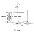
- the prior-art semiconductor memory device having such an internal supply-voltage step-down circuit is shown in Fig. 1.
- the memory device is composed of a memory cell array 4 and as peripheral circuits, an address buffer 3-1, a row decoder 3-2, a column decoder 3-3 and an input/output circuit 3-4 in a known manner.
- the memory device further comprises a supply-voltage step-down circuit 1 which receives an external power voltage Vcc which is usual set at 5 V and generates a reduced value of an internal supply voltage V 1NT , a value of which is typically 3 to 4 V.
- the internal voltage V INT is fed to an internal power supply wiring 5 coupled to the peripheral circuits 3-1 to 3-4 and the memory cell array 4.
- BT burn-in test
- a semiconductor device is exposed to high temperature (on the order of +120°C) and high voltage (on the order of + 7 V) for a long time (several to several tens hours), thereby to remove initial defective units.
- the prior-art semiconductor memory device drops the external supply voltage therein and then uses the dropped voltage in order to ensure the reliabilities of the transistors, the high voltage lowers within the device even during the burn-in test stated above, resulting in the problem that initial defective units cannot be effectively removed.
- the external supply voltage raised to the high voltage e.g. 7 V to the internal elements such as transistors in the burn-in test because there is inevitably the internal supply-voltage step-down circuit present between the external supply voltage terminal and the internal elements, and the internal supply-voltage step-down circuit produces the regulated or reduced value of the internal supply voltage to be fed to the internal elements.
- It is an object of the present invention is to provide a semiconductor device which can directly apply an external supply voltage to internal elements when a burn-in test is performed.
- the semiconductor device comprises an internal circuit, an internal supply voltage generator receiving an external supply voltage through an external supply voltage terminal and generating an internal supply voltage at its output end, a temperature sensing circuit for sensing an ambient temperature, and a connection circuit for connecting the internal circuit to the output end of the internal supply voltage generator when the ambient temperature is below a predetermined value and to the external supply voltage terminal when the ambient temperature is at the predetermined value or more.
- an internal supply voltage generator receiving an external supply voltage through an external supply voltage terminal and generating an internal supply voltage at its output end
- a temperature sensing circuit for sensing an ambient temperature
- a connection circuit for connecting the internal circuit to the output end of the internal supply voltage generator when the ambient temperature is below a predetermined value and to the external supply voltage terminal when the ambient temperature is at the predetermined value or more.
- a semiconductor device having a supply-voltage step-down circuit which lowers a supply voltage externally fed and then feeds the lowered supply voltage to an internal circuit, an element which is connected between two voltage sources and of which electric characteristic changes according to an ambient temperature thereof, and a detector circuit which detects the change of the electric characteristic of the element and which has its output signal inverted when the ambient temperature has reached a predetermined temperature, thereby to cancel the function of said supply-voltage internal step-down circuit and to feed the externally-fed supply voltage to said internal circuits.
- a change in the ambient temperature leads to a change in the electric characteristic of the element, and the detector circuit monitors this change.
- the output of the detector circuit is inverted. It can therefore be known from the output of the detector circuit that the ambient temperature has reached the predetermined one.
- the temperature detection circuit of such construction is built in a semiconductor device so as to control the function of the supply-voltage internal step-down circuit, the voltage to be fed to the other internal circuits during an ordinary operation can be changed from that during the burn-in test.
- Fig. 2 illustrates a semiconductor memory device according to a first embodiment of the present invention.
- Fig. 2 the same constituents as in the prior-art example have the same numerals assigned thereto, and their description will be omitted.
- a difference from the prior-art example is the incorporation of a temperature detection circuit 2, a first switch formed of a P-channel MOS transistor QP1 coupled between the power supply terminal Vcc and the internal power supply line 5, and a second switch formed of a P-channel transistor QP2 and an inverter 6 for generating a signal ⁇ complementary to an output signal q) of the temper detecting circuit 2.
- this temperature detection circuit 2 includes a resistance element R of large temperature coefficient such as of high-resistivity polycrystalline silicon, an N-channel type MOS transistor Q 1 which has its gate connected to a voltage source, its source to a ground node, and its drain to the resistance element R, and an inverter 7 which is connected to the node N between the resistance element R and the transistor Q 1 and which generates an output signal q).
- the voltage value of the node N is determined by the ratio between the resistance of the resistance element R and the on-resistance of the transistor Q 1 .
- the resistance element R is made of the high-resistivity polycrystalline silicon or the like, the temperature coefficient thereof is very large, and the resistance value thereof becomes smaller extraordinarily at higher temperatures. Accordingly, the voltage of the node N rises with a temperature rise as shown in Fig. 4.
- the temperature coefficient of the N-channel type MOS transistor Q 1 is very small as compared with that of the resistance element R and is therefore negligible. Thus, it may well be considered that the temperature characteristic of the voltage of the node N is determined only by the temperature characteristic of the resistance element R.
- the output signal ⁇ of the detection circuit 2 is at a high (Vcc) level and therefore the signal ⁇ is at a low (ground) level. Therefore, the transistor QP2 is rendered conductive and the transistor QP1 is rendered non-conductive so that the output of the internal supply-voltage step-down circuit 1 i.e. the internal supply voltage is applied to the internal power supply line 5.
- the output 4) is inverted to the low level as shown in Fig. 4.
- the transistors QP1 and QP2 are rendered conductive and non-conductive, respectively so that the supply-voltage 1 step-down circuit 1 is bypassed by the transistor QP1.
- the temperature at which the threshold voltage V th of the inverter 5 is reached is preset as the temperature (for example, 120°C) of a burn-in test, the supply voltage step-down 1 can be cancelled only during the burn-in test, and a semiconductor memory device involving initial defects can be removed beforehand.
- this embodiment is featured in that an N-channel MOS transistor Q 2 is inserted between the node N and the transistor 0 1 and the inverter 5 is replaced with a NAND gate 8, and the transistor Q 2 and the NAND gate 6 are controlled by a chip-selector signal CS.
- the chip-select signal CS When the chip-select signal CS is at its high level, the operation of the circuit dependent upon the temperature is quite the same as with the temperature detection circuit 2 in the first embodiment, and hence, its description will be omitted.
- the chip-select signal CS when the chip-select signal CS is at its low level, the transistor Q 2 is turned “off", and the signal q) from the NAND gate 8 is fixed at its high level. Accordingly, any through current does not flow at all in the temperature detection circuit 2' shown in Fig. 5, in a stand-by state of the memory device.
- This embodiment has an advantage that current consumption can be rendered substantially zero merely by setting a chip-select internal signal CS at a low level.
- each of the embodiments has explained cancellation of the function of the supply voltage step-down circuit built in the memory device
- the present invention is also applicable to variety of semiconductor device other than memory devices.
Landscapes
- Engineering & Computer Science (AREA)
- General Engineering & Computer Science (AREA)
- Physics & Mathematics (AREA)
- General Physics & Mathematics (AREA)
- Dram (AREA)
- For Increasing The Reliability Of Semiconductor Memories (AREA)
- Testing Or Measuring Of Semiconductors Or The Like (AREA)
- Semiconductor Integrated Circuits (AREA)
- Tests Of Electronic Circuits (AREA)
- Read Only Memory (AREA)
Applications Claiming Priority (2)
| Application Number | Priority Date | Filing Date | Title |
|---|---|---|---|
| JP229992/90 | 1990-08-30 | ||
| JP22999290A JP3158420B2 (ja) | 1990-08-30 | 1990-08-30 | 温度検出回路および温度検出回路を備えた半導体装置 |
Publications (3)
| Publication Number | Publication Date |
|---|---|
| EP0473193A2 true EP0473193A2 (fr) | 1992-03-04 |
| EP0473193A3 EP0473193A3 (en) | 1992-07-08 |
| EP0473193B1 EP0473193B1 (fr) | 1997-04-02 |
Family
ID=16900909
Family Applications (1)
| Application Number | Title | Priority Date | Filing Date |
|---|---|---|---|
| EP91114672A Expired - Lifetime EP0473193B1 (fr) | 1990-08-30 | 1991-08-30 | Dispositif semi-conducteur comprenant un circuit de détéction de la température |
Country Status (5)
| Country | Link |
|---|---|
| US (1) | US5285418A (fr) |
| EP (1) | EP0473193B1 (fr) |
| JP (1) | JP3158420B2 (fr) |
| KR (1) | KR940009349B1 (fr) |
| DE (1) | DE69125437T2 (fr) |
Cited By (6)
| Publication number | Priority date | Publication date | Assignee | Title |
|---|---|---|---|---|
| EP0565156A3 (en) * | 1992-04-09 | 1994-11-23 | Ibm | Voltage burn-in scheme for bicmos circuits |
| DE19524616A1 (de) * | 1995-07-06 | 1997-01-09 | Telefunken Microelectron | Verfahren zur Testung einer Übertemperaturerkennung in einem integrierten Schaltkreis |
| FR2857091A1 (fr) * | 2003-07-01 | 2005-01-07 | St Microelectronics Sa | Procede de detection de la temperature d'un circuit integre, et circuit integre correspondant |
| EP1531493A3 (fr) * | 1997-09-19 | 2005-09-28 | Integrated Memory Technologies, Inc. | Ensemble memoire flash |
| CN108885886A (zh) * | 2015-09-28 | 2018-11-23 | 西部数据技术公司 | 基于老化状况的存储器裸片温度调节 |
| CN109239618A (zh) * | 2018-09-06 | 2019-01-18 | 凌云光技术集团有限责任公司 | 一种光源电源全自动老化系统及方法 |
Families Citing this family (10)
| Publication number | Priority date | Publication date | Assignee | Title |
|---|---|---|---|---|
| US5440520A (en) * | 1994-09-16 | 1995-08-08 | Intel Corporation | Integrated circuit device that selects its own supply voltage by controlling a power supply |
| JP3648304B2 (ja) * | 1995-11-17 | 2005-05-18 | 株式会社東芝 | 不揮発性半導体記憶装置 |
| JPH11185498A (ja) * | 1997-12-24 | 1999-07-09 | Mitsubishi Electric Corp | スタティック型半導体記憶装置 |
| US6060895A (en) * | 1998-04-20 | 2000-05-09 | Fairchild Semiconductor Corp. | Wafer level dielectric test structure and related method for accelerated endurance testing |
| US6021076A (en) * | 1998-07-16 | 2000-02-01 | Rambus Inc | Apparatus and method for thermal regulation in memory subsystems |
| US6453218B1 (en) * | 1999-03-29 | 2002-09-17 | Intel Corporation | Integrated RAM thermal sensor |
| DE10036914A1 (de) * | 2000-07-28 | 2002-02-14 | Infineon Technologies Ag | Integrierte Schaltung mit Temperatursensor |
| KR100577560B1 (ko) * | 2003-12-23 | 2006-05-08 | 삼성전자주식회사 | 온도감지 데이터에 응답하는 내부회로를 갖는 반도체메모리장치 |
| KR20130059003A (ko) * | 2011-11-28 | 2013-06-05 | 삼성전자주식회사 | 반도체 테스트 보드 및 반도체 보드 |
| KR102918304B1 (ko) * | 2022-06-29 | 2026-01-27 | 에스케이하이닉스 주식회사 | Pbti를 모니터링하는 테스트 회로 및 이의 동작 방법 |
Family Cites Families (4)
| Publication number | Priority date | Publication date | Assignee | Title |
|---|---|---|---|---|
| US4278873A (en) * | 1980-02-04 | 1981-07-14 | General Electric Company | Temperature-responsive control means |
| JPS60253090A (ja) * | 1984-05-30 | 1985-12-13 | Hitachi Ltd | 半導体装置 |
| US4730228A (en) * | 1986-03-21 | 1988-03-08 | Siemens Aktiengesellschaft | Overtemperature detection of power semiconductor components |
| JPH07105160B2 (ja) * | 1989-05-20 | 1995-11-13 | 東芝マイクロエレクトロニクス株式会社 | 半導体記憶装置 |
-
1990
- 1990-08-30 JP JP22999290A patent/JP3158420B2/ja not_active Expired - Fee Related
-
1991
- 1991-08-30 US US07/753,134 patent/US5285418A/en not_active Expired - Lifetime
- 1991-08-30 DE DE69125437T patent/DE69125437T2/de not_active Expired - Fee Related
- 1991-08-30 EP EP91114672A patent/EP0473193B1/fr not_active Expired - Lifetime
- 1991-08-30 KR KR1019910015078A patent/KR940009349B1/ko not_active Expired - Fee Related
Cited By (8)
| Publication number | Priority date | Publication date | Assignee | Title |
|---|---|---|---|---|
| EP0565156A3 (en) * | 1992-04-09 | 1994-11-23 | Ibm | Voltage burn-in scheme for bicmos circuits |
| DE19524616A1 (de) * | 1995-07-06 | 1997-01-09 | Telefunken Microelectron | Verfahren zur Testung einer Übertemperaturerkennung in einem integrierten Schaltkreis |
| DE19524616C2 (de) * | 1995-07-06 | 1998-02-05 | Telefunken Microelectron | Verfahren zur Testung einer Übertemperaturerkennung in einem integrierten Schaltkreis |
| EP1531493A3 (fr) * | 1997-09-19 | 2005-09-28 | Integrated Memory Technologies, Inc. | Ensemble memoire flash |
| FR2857091A1 (fr) * | 2003-07-01 | 2005-01-07 | St Microelectronics Sa | Procede de detection de la temperature d'un circuit integre, et circuit integre correspondant |
| CN108885886A (zh) * | 2015-09-28 | 2018-11-23 | 西部数据技术公司 | 基于老化状况的存储器裸片温度调节 |
| CN108885886B (zh) * | 2015-09-28 | 2022-05-31 | 西部数据技术公司 | 基于老化状况的存储器裸片温度调节 |
| CN109239618A (zh) * | 2018-09-06 | 2019-01-18 | 凌云光技术集团有限责任公司 | 一种光源电源全自动老化系统及方法 |
Also Published As
| Publication number | Publication date |
|---|---|
| DE69125437T2 (de) | 1997-08-07 |
| US5285418A (en) | 1994-02-08 |
| KR920005322A (ko) | 1992-03-28 |
| KR940009349B1 (ko) | 1994-10-07 |
| JPH04111335A (ja) | 1992-04-13 |
| EP0473193B1 (fr) | 1997-04-02 |
| DE69125437D1 (de) | 1997-05-07 |
| JP3158420B2 (ja) | 2001-04-23 |
| EP0473193A3 (en) | 1992-07-08 |
Similar Documents
| Publication | Publication Date | Title |
|---|---|---|
| EP0157905B1 (fr) | Dispositif semi-conducteur | |
| US4833341A (en) | Semiconductor device with power supply voltage converter circuit | |
| US4937700A (en) | Semiconductor integrated circuit with a circuit limiting an input voltage to a predetermined voltage | |
| US5285418A (en) | Semiconductor device having a temperature detection circuit | |
| JP2995204B2 (ja) | Mos技術の高圧レベル検出回路 | |
| US6434078B1 (en) | Semiconductor device allowing external setting of internal power supply voltage generated by a voltage down converter at the time of testing | |
| US7525332B2 (en) | On-chip substrate regulator test mode | |
| US4868483A (en) | Power voltage regulator circuit | |
| US6624685B2 (en) | Level detection by voltage addition/subtraction | |
| EP0399240A2 (fr) | Dispositif de mémoire à semi-conducteur | |
| US6564351B2 (en) | Circuit and method for testing an integrated circuit | |
| US5815429A (en) | Antifuse programming method and apparatus | |
| KR890004408B1 (ko) | 반도체기억장치의 메모리 셀(cell) 캐패시터 전압인가회로 | |
| JP2881729B2 (ja) | 半導体メモリのバーンイン感知回路 | |
| US5786719A (en) | Mode setting circuit and mode setting apparatus used to select a particular semiconductor function | |
| US6388926B1 (en) | Integrated circuit having forced substrate test mode with improved substrate isolation | |
| US6271692B1 (en) | Semiconductor integrated circuit | |
| US6606264B2 (en) | Programmable circuit and its method of operation | |
| KR100196609B1 (ko) | 반도체 집적 회로 장치 | |
| US6522591B2 (en) | Semiconductor memory circuit | |
| US5905682A (en) | Method and apparatus for biasing the substrate of an integrated circuit to an externally adjustable voltage | |
| US6822470B2 (en) | On-chip substrate regulator test mode | |
| KR100253646B1 (ko) | 반도체메모리장치의시그너쳐회로. | |
| JPH03289568A (ja) | 電圧検出装置 | |
| JP3256689B2 (ja) | 半導体集積回路 |
Legal Events
| Date | Code | Title | Description |
|---|---|---|---|
| PUAI | Public reference made under article 153(3) epc to a published international application that has entered the european phase |
Free format text: ORIGINAL CODE: 0009012 |
|
| 17P | Request for examination filed |
Effective date: 19910830 |
|
| AK | Designated contracting states |
Kind code of ref document: A2 Designated state(s): DE FR GB |
|
| PUAL | Search report despatched |
Free format text: ORIGINAL CODE: 0009013 |
|
| AK | Designated contracting states |
Kind code of ref document: A3 Designated state(s): DE FR GB |
|
| 17Q | First examination report despatched |
Effective date: 19950210 |
|
| GRAG | Despatch of communication of intention to grant |
Free format text: ORIGINAL CODE: EPIDOS AGRA |
|
| GRAH | Despatch of communication of intention to grant a patent |
Free format text: ORIGINAL CODE: EPIDOS IGRA |
|
| GRAH | Despatch of communication of intention to grant a patent |
Free format text: ORIGINAL CODE: EPIDOS IGRA |
|
| GRAA | (expected) grant |
Free format text: ORIGINAL CODE: 0009210 |
|
| AK | Designated contracting states |
Kind code of ref document: B1 Designated state(s): DE FR GB |
|
| REF | Corresponds to: |
Ref document number: 69125437 Country of ref document: DE Date of ref document: 19970507 |
|
| ET | Fr: translation filed | ||
| PLBE | No opposition filed within time limit |
Free format text: ORIGINAL CODE: 0009261 |
|
| STAA | Information on the status of an ep patent application or granted ep patent |
Free format text: STATUS: NO OPPOSITION FILED WITHIN TIME LIMIT |
|
| 26N | No opposition filed | ||
| REG | Reference to a national code |
Ref country code: GB Ref legal event code: IF02 |
|
| REG | Reference to a national code |
Ref country code: GB Ref legal event code: 732E |
|
| REG | Reference to a national code |
Ref country code: FR Ref legal event code: TQ |
|
| REG | Reference to a national code |
Ref country code: GB Ref legal event code: 732E |
|
| REG | Reference to a national code |
Ref country code: FR Ref legal event code: TP |
|
| PGFP | Annual fee paid to national office [announced via postgrant information from national office to epo] |
Ref country code: DE Payment date: 20080912 Year of fee payment: 18 |
|
| PGFP | Annual fee paid to national office [announced via postgrant information from national office to epo] |
Ref country code: FR Payment date: 20080818 Year of fee payment: 18 |
|
| PGFP | Annual fee paid to national office [announced via postgrant information from national office to epo] |
Ref country code: GB Payment date: 20080903 Year of fee payment: 18 |
|
| GBPC | Gb: european patent ceased through non-payment of renewal fee |
Effective date: 20090830 |
|
| REG | Reference to a national code |
Ref country code: FR Ref legal event code: ST Effective date: 20100430 |
|
| PG25 | Lapsed in a contracting state [announced via postgrant information from national office to epo] |
Ref country code: DE Free format text: LAPSE BECAUSE OF NON-PAYMENT OF DUE FEES Effective date: 20100302 Ref country code: FR Free format text: LAPSE BECAUSE OF NON-PAYMENT OF DUE FEES Effective date: 20090831 |
|
| PG25 | Lapsed in a contracting state [announced via postgrant information from national office to epo] |
Ref country code: GB Free format text: LAPSE BECAUSE OF NON-PAYMENT OF DUE FEES Effective date: 20090830 |