EP0473409A2 - Circuit logique Bicmos - Google Patents
Circuit logique Bicmos Download PDFInfo
- Publication number
- EP0473409A2 EP0473409A2 EP91307873A EP91307873A EP0473409A2 EP 0473409 A2 EP0473409 A2 EP 0473409A2 EP 91307873 A EP91307873 A EP 91307873A EP 91307873 A EP91307873 A EP 91307873A EP 0473409 A2 EP0473409 A2 EP 0473409A2
- Authority
- EP
- European Patent Office
- Prior art keywords
- logic circuit
- cmos logic
- bipolar transistor
- npn bipolar
- gate
- Prior art date
- Legal status (The legal status is an assumption and is not a legal conclusion. Google has not performed a legal analysis and makes no representation as to the accuracy of the status listed.)
- Granted
Links
- 238000010586 diagram Methods 0.000 description 8
- 238000007599 discharging Methods 0.000 description 5
- 230000000694 effects Effects 0.000 description 3
- 230000000630 rising effect Effects 0.000 description 2
- 230000001154 acute effect Effects 0.000 description 1
- 230000003247 decreasing effect Effects 0.000 description 1
Images



Classifications
-
- H—ELECTRICITY
- H03—ELECTRONIC CIRCUITRY
- H03K—PULSE TECHNIQUE
- H03K19/00—Logic circuits, i.e. having at least two inputs acting on one output; Inverting circuits
- H03K19/0008—Arrangements for reducing power consumption
- H03K19/0013—Arrangements for reducing power consumption in field effect transistor circuits
-
- H—ELECTRICITY
- H03—ELECTRONIC CIRCUITRY
- H03K—PULSE TECHNIQUE
- H03K19/00—Logic circuits, i.e. having at least two inputs acting on one output; Inverting circuits
- H03K19/02—Logic circuits, i.e. having at least two inputs acting on one output; Inverting circuits using specified components
- H03K19/08—Logic circuits, i.e. having at least two inputs acting on one output; Inverting circuits using specified components using semiconductor devices
- H03K19/094—Logic circuits, i.e. having at least two inputs acting on one output; Inverting circuits using specified components using semiconductor devices using field-effect transistors
- H03K19/0944—Logic circuits, i.e. having at least two inputs acting on one output; Inverting circuits using specified components using semiconductor devices using field-effect transistors using MOSFET or insulated gate field-effect transistors, i.e. IGFET
- H03K19/09448—Logic circuits, i.e. having at least two inputs acting on one output; Inverting circuits using specified components using semiconductor devices using field-effect transistors using MOSFET or insulated gate field-effect transistors, i.e. IGFET in combination with bipolar transistors [BIMOS]
Definitions
- the present invention relates to a Bipolar-CMOS (BiCMOS) logic circuit and, more particularly, to a BiCMOS logic circuit which is suitable for operation under low power supply voltage.
- BiCMOS Bipolar-CMOS
- BiCMOS logic circuits In recent years, with advancement in speed of operation of integrated circuits, the demand for BiCMOS logic circuits is increasing. In one type of BiCMOS logic circuit which is recently attracting attention, there are an NPN bipolar transistor and N-channel MOSFETs (hereinafter referred to as "NMOSs") which are connected with each other in series and having an output terminal disposed between them. In another type of a typical conventional BiCMOS logic,circuit, a similar arrangement is with two NPN bipolar transistors which are connected with each other in series. Generally, an advantage of BiCMOS logic circuits resides in their ability to drive a large load capacitance. However, in both the types of conventional BiCMOS logic circuits, there is a problem or disadvantage in that their operation speed under low power supply voltage is slow. Full description of such conventional BiCMOS logic circuits and the problems existing therein will be fully explained later.
- An object of the present invention is to provide a BiCMOS logic circuit which is capable of operating at a high speed under low power supply voltage.
- Another object of the invention is to provide a BiCMOS logic circuit in which it is possible to decrease the size of an NMOS logic unit, to reduce input capacitance and to decrease fan-out dependency on average delay times.
- a BiCMOS logic circuit comprising:
- a BiCMOS logic circuit comprising:
- the BiCMOS logic circuit includes an NPN bipolar transistor and an N-channel MOSFET (hereinafter referred to as "NMOS") which are connected with each other in series with an intermediate point between them being made an output terminal.
- NMOS N-channel MOSFET
- Fig. 1 diagrammatically shows such a conventional BiCMOS logic circuit which is designed for use under low power supply voltage and which includes the NPN bipolar transistor and the NMOSs connected in series.
- a CMOS logic circuit 21 conducts logical NAND operation between input signals S 1 and S 2 applied to input terminals T 1 and T 2 , respectively.
- the CMOS logic circuit 21 is formed such that a parallel circuit of P-channel MOSFETs (hereinafter referred to as "PMOSs") 23, 24 and a serial circuit of NMOSs 25, 26 are connected in series between a power source terminal V DD and a ground terminal.
- the input signal S 1 applied to the input terminal T 1 is inputted to gates of the PMOS 24 and the NMOS 25, and the input signal S 2 applied to the input terminal T 2 is inputted to gates of the PMOS 23 and the NMOS 26.
- a connection between common drains of the PMOSs 23, 24 and a drain of the NMOS 25 is an output node of the CMOS logic circuit 21.
- This output node is connected to a base of an NPN bipolar transistor 29 whose collector is connected to the power source terminal V DD and whose emitter is connected to an output terminal To for outputting an output signal So.
- Connected between the emitter of the NPN bipolar transistor 29 and the ground terminal is an NMOS logic section 22 formed by a serial circuit of the NMOSs 27 and 28 to which the input signals S 1 and S 2 are respectively inputted.
- the output signal So will be in its "0" state.
- this state changes to a state wherein at least either of the input signals S 1 and S 2 is "0"
- at least one of the PMOSs 23 and 24 becomes conductive and at least one of the NMOSs 25 and 26 becomes non-conductive, so that the potential at the output node of the CMOS logic circuit 21 rises towards the potential of the power source voltage V DD and accordingly the NPN bipolar transistor 29 becomes conductive due to the rise of its base potential.
- the NMOSs 27 and 28 becomes non-conductive, the NMOS logic section 22 loses its current passage.
- the potential of the output signal So rises and reaches the potential which is lowered from the V DD potential by the amount of the built-in potential V F of the emitter-base junction of the NPN bipolar transistor 29.
- the level of the potential of the output signal So becomes "1".
- the NMOSs for discharging purposes must of necessity be of large size and, as a result, the input capacitance inevitably becomes very large. This presents a problem in that, as the input capacitance increases, there is an increase in the number of fan-outs resulting in a marked increase in the average delay times Tpd.
- the BiCMOS logic circuit exemplified in Fig. 1 shows that of a two-input NAND gate type.
- the numberof inputs increases, there will be an increase in the number of stages in series of the NMOSs forming the discharging passage.
- the sizes of the NMOSs be further increased for them to be able to operate at a high speed.
- the input capacitance is further increased and the fan-out dependency on Tpd is shown to have an acute increase and these are accounted for as elements for capability limitations of circuits in practical use.
- the present invention thus aims at providing a BiCMOS logic circuit which overcomes the above explained problems and in which the input capacitance can be decreased and the fan-out dependency on the average delay times can be restricted.
- NMOSs included in a CMOS logic circuit become conductive and the output of the CMOS logic circuit rises
- an NMOS logic section first becomes conductive and charges a gate of a first NMOS through the NMOS logic section. Subsequently, the gate of the first NMOS is charged through a PMOS.
- the amount which is to be charged through the NMOS logic section is only for the gate capacitance of the first NMOS and, more over, it is sufficient if the NMOS logic section operates only for initial charging, so that the ON-resistance of the NMOS logic section can be of a large value. Therefore, in the BiCMOS according to the invention, the size of the NMOS logic section can be made small and also the input capacitance can be made smaller as compared with that in the conventional circuit.
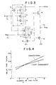
- Fig. 3 diagrammatically shows a two-input NAND type BiCMOS logic circuit which is designed for operation under low power supply voltage and which includes an NPN bipolar transistor and an NMOS connected with each other in series.
- a CMOS logic circuit 1 is one from which a logical NAND signal of input signals S 1 and S 2 is outputted and in which a parallel circuit of PMOSs 3, 4 and a serial circuit of NMOSs 5, 6 are connected in series between a power source terminal V DD and a ground terminal.
- the input signal S 1 is inputted to gates of the PMOS 3 and the NMOS 5 and the input signal S 2 is inputted to gates of the PMOS 4 and NMOS 6.
- a connection node between common drains of the PMOSs 3, 4 and a drain of the NMOS 5 is an output node of the CMOS logic circuit 1.
- the output node of the CMOS logic circuit 1 is connected to a base of an NPN bipolar transistor 9.
- the NPN bipolar transistor 9 has its collector connected to the power source terminal V DD and its emitter connected to an output terminal To for an output signal So.
- An NMOS 12 is connected between the emitter of the NPN bipolar transistor 9 and the ground terminal.
- NMOS logic section 2 formed by NMOSs 7, 8 and a PMOS 11 which is connected therewith in parallel.
- the input signals S 1 and S 2 are respectively inputted to the gates of the NMOSs 7 and 8.
- the gate of the PMOS 11 is connected to the base of the NPN bipolar transistor 9.
- an NMOS 10 whose gate is connected to the base of the NPN bipolar transistor 9.
- the NMOS logic section 2 and the NMOS 10 constitute a partial circuit of the two-input AND logic circuit. Consequently, there occurs, push-pull operation between the NPN bipolar transistor 9 whose base is connected to the output node of the CMOS logic circuit 1 and the NMOS 12 for output driving whose gate is connected to the output node of the circuit constituted by the NMOS logic section 2 and the NMOS 10.
- the PMOS 11 charges the gate of the NMOS 12 up to the V DD potential and operates to enhance the driving capability of the NMOS 12.
- the NMOS 10 turns to its non-conductive state and the PMOS 10 turns to its conductive state
- the gate potential of the NMOS 12 quickly rises towards the potential of the power source voltage V DD thereby causing the NMOS 12 to be in a deeply conductive state and, as a result, the potential of the output terminal To falls quickly towards the ground potential resulting in the potential being in its "0" level.
- the gate of the NMOS 12 is charged first through the NMOS logic section 2 and later through the PMOS 11. If the PMOS 11 is not present, the gate of the NMOS 12 will have to be charged solely by the NMOS logic section 2 so that the gate potential thereof will rise only to the potential in which the value is lowered from the high levels of the input signals S 1 , S 2 by the threshold voltage V TN of the NMOSs and this means that the driving capability of the NMOS 12 will be lowered.
- the NMOS logic section 2 is not present, the potential change in the CMOS logic circuit 1 will be supplied to the gate of the NMOS 12 after being further inverted by a CMOS inverter constituted by the PMOS 11 and the NMOS 10, the time required before the start of the conduction of the NMOS 12 will be longer. According to the embodiment of the invention, however, since the NMOS logic section 2 and the PMOS 11 are both present, it is possible to expedite the start of the conduction of the NMOS 12 and also to maintain the driving capability at a high level.
- the ON-resistance at the time of the conduction of the NMOSs 7 and 8 constituting the NMOS logic section 2 can be several times larger in its value as compared with that in the NMOSs 27, 28 of the conventional circuit as shown in Fig. 1.
- the sizes of the NMOSs 7 and 8 can be made small, thereby realizing a BiCMOS circuit having a small input capacitance as compared with the conventional circuit.
- Fig. 4 graphically shows a relationship between the number of fan-outs and the delay times Tpd of the circuit according to the present embodiment. As apparent from the graph, it is due to the input capacitance reduction effect that, despite an increase in the number of fan-outs, the ratio of an increase in the Tpd is small in the embodiment of the invention. It can be appreciated that the operation at a higher speed is enabled when the number of fan-outs is larger as compared with the conventional circuit.
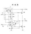
- a BiCMOS circuit includes a first CMOS logic circuit 1a a formed by a pair of PMOSs 3a, 4a and a pair of NMOSs 5a, 5b and a second CMOS circuit 1 b similarly formed by a pair of PMOSs 3b, 4b and a pair of NMOSs 5b, 6b, and these circuits constitute the same two-input NAND circuit.
- the differences in this embodiment from the first embodiment reside in that, whereas in the first embodiment, the NPN bipolar transistor 9 and the NMOS 10 and the PMOS 11 are driven by the CMOS logic circuit 1, in this second embodiment the first CMOS logic circuit 1a is provided exclusively for driving the base of the NPN bipolar transistor 9 and in that the second CMOS logic circuit 1 b is provided exclusively for driving the gates of the NMOS 10 and the PMOS 11.
- the configuration and operation as explained with reference to Fig. 3 are the same in this embodiment.
- the output load capacitance to be driven by the first CMOS logic circuit 1 a is the base capacitance of the NPN bipolar transistor 9 and also the output load capacitance to be driven by the second CMOS logic circuit 1 b is only the capacitance of the gates of the NMOS 10 and the PMOS 11.
- the NMOSs 5a, 6a of the first CMOS logic circuit 1a are used exclusively for discharging the charge at the base of the NPN bipolar transistor 9 which makes it unnecessary to reduce the ON-resistance of the transistor 9 and which allows the use of an NMOS of a small size.
- the PMOSs 3b, 4b of the second CMOS logic circuit 1 b are also exclusively for making the NMOS 10 conductive and discharging the charge at the gate of the NMOS 12, it is possible to use the PMOSs of a smaller size as compared with the PMOSs 3a, 4a of the first CMOS logic circuit 1a. Therefore, there is an advantage in this embodiment as compared with the first embodiment in that the circuit can operate at a higher speed and that the input capacitance can be suppressed to a smaller increase.
- the BiCMOS logic circuit includes the NMOS connected in series with the NPN bipolar transistor.
- the BiCMOS logic circuit includes two NPN bipolar transistors connected with each other in series and having an output terminal therebetween.
- CMOS logic circuit 51 conducts a logical NAND operation between input signals S 1 and S 2 .
- the CMOS logic circuit is constructed such that a parallel circuit of a pair of PMOSs 53, 54 and a serial circuit of NMOSs 55, 56 are connected in series between a power source terminal V DD and a ground terminal.
- the input signal S 1 is inputted to gates of the PMOS 53 and the NMOS 55 and the input signal S 2 is inputted to gates of the PMOS 54 and the NMOS 56.
- a connection between common drains of the PMOSs 53, 54 and a drain of the NMOS 55 is an output node of the CMOS logic circuit 51. This output node is connected to a base of an NPN bipolar transistor 59.
- the NPN bipolar transistor 59 has its collector connected to the power source terminal V DD and its emitter connected to an output terminal To for an output signal So. Between the emitter of the NPN bipolar transistor 59 and the ground terminal, there is an NPN bipolar transistor 62.
- NMOS logic section 52 formed by a serial circuit of NMOSs 57 and 58 to which the input signals S 1 and S 2 are respectively inputted.
- NMOS 60 whose gate is connected to the output node of the CMOS logic circuit 51.
- the NMOS logic section 52 and the NMOS 60 that produce an output whose phase is opposite to that of the CMOS logic circuit 51 whereby the NPN bipolar transistors 59 and 62 performs a push-pull operation.
- the output signal So will be in its "0" state.
- this state changes to a state wherein at least either of the input signals S 1 and S 2 is "0”
- at least one of the PMOSs 53 and 54 becomes conductive and at least one of the NMOSs 55 and 56 becomes non-conductive, so that the output node of the CMOS logic circuit 51, that is the base potential of the NPN bipolar transistor 59, rises towards the potential of the power source voltage V DD as a result of being charged by at least one of the PMOSs 53 and 54. Consequently, the NPN bipolar transistor 59 becomes conductive.
- the NMOS logic section 52 one of the NMOSs 57 and 58 becomes non-conductive.
- the NMOS 60 becomes conductive.
- the base potential of the NPN bipolar transistor 62 falls towards the ground potential thereby causing the NPN bipolar transistor 62 to become non-conductive.
- the potential of the output signal So rapidly rises and reaches a potential which is lower than the V DD potential by the amount of the built-in potential V F of the emitter-base junction of the NPN bipolar transistor 59.
- the level of the potential of the output signal So becomes "1".
- the base potential of the NPN bipolar transistor 62 starts rising towards the potential which is lower than the potential of the input signals of S 1 , S 2 of "1" level by the amount of the threshold voltages of the NMOSs 57 and 58.
- the NPN bipolar transistor 62 becomes conductive.
- the potential of the output signal So falls towards the potential which is higher by the amount of V F from the ground potential and reaches its "0" level.
- the base potential of the NPN bipolar transistor 62 rises once but, along with the falling of the level of the output signal So, falls again and eventually becomes the same as the level of the output signal So.
- the base potential of the NPN bipolar transistor 62 does not rise beyond the potential which is lower by the amount of the threshold voltages of the NMOSs than the "1" level potential of the input signals S 1 , S 2 , the base potential of the NPN bipolar transistor 62 in the case of the input terminals being connected to outputs of other BiCMOS logic circuits rises only up to (V DD - V F - V TN ) (wherein V TN is the threshold voltage of the NMOSs).
- the average delay time Tpd in the BiCMOS logic circuit is shown to have characteristics that it increases very rapidly when the power source voltage V ⁇ is in the order of 3 V.
- the conventional BiCMOS logic circuit can operate at a high speed if the voltage is 5 V which is a conventional standard voltage, the operation speed suddenly deteriorates at a power source voltage in the order of 3 V.
- the advantage in the BiCMOS logic circuit over the CMOS logic circuit that is, the advantage in the capability of driving a large load capacitance at a high speed, is lost and this means that such advantage or superiority over the CMOS logic circuit can no longer be maintained if the standard power source voltage were to be 3.3 V which is aimed at as a possible standard power source voltage in the future.
- the object of the present invention is to provide a BiCMOS which is capable of operating at a high speed under a low power source voltage.
- the NMOSs constituting the CMOS logic circuit becomes conductive and, when the output of the CMOS logic circuit rises, the base of the second NPN bipolar transistor is charged by both the NMOS logic section and the PMOS connected thereto in parallel. Therefore, the base potential of the second NPN bipolar transistor is charged to a level higher than in a conventional circuit. This means that the circuit according to the present invention can operate at a higher speed under a lower power source voltage.
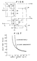
- Fig. 6 diagrammatically shows a two-input NAND type BiCMOS logic circuit which is designed for operation under low power supply voltage and which includes a first NPN bipolar transistor and a second NPN bipolar transistor connected with each other in series.
- a CMOS logic circuit 1 is one from which a logical NAND signal between input signals S 1 and S 2 is outputted and in which a parallel circuit of a pair of PMOSs 33, 34 and a serial circuit of NMOSs 35, 36 are connected in series between a power source terminal V DD and a ground terminal.
- the input signal S 1 is inputted to gates of the PMOS 33 and the NMOS 35 and the input signal S 2 is inputted to gates of the PMOS 34 and the NMOS 36.
- a connection node between common drains of the PMOSs 33, 34 and a drain of the NMOS 35 is an output node of the CMOS logic circuit 1.
- the output node of the CMOS logic circuit 1 is connected to a base of an NPN bipolar transistor 39.
- the NPN bipolar transistor 39 has its collector connected to the power source terminal V DD and its emitter connected to an output terminal To for outputting an output signal So.
- An NPN bipolar transistor 42 is connected between the emitter of the NPN bipolar transistor 39 and the ground terminal.
- NMOS logic section 2 formed by NMOSs 37, 38 and a PMOS 41 connected thereto in parallel.
- the input signals S 1 and S 2 are respectively inputted to the gates of the NMOSs 37 and 38.
- the gate of the PMOS 41 is connected to the base of the NPN bipolar transistor 39.
- an NMOS 40 is connected between the base of the NPN bipolar transistor 42 and the ground terminal. The gate of the NMOS 40 is connected to the base of the NPN bipolar transistor 39.
- the NMOS logic section 2 and the NMOS 40 constitute a partial circuit of the two-input AND logic circuit. There occurs a push-pull operation between the NPN bipolar transistor 39 whose base is connected to the output node of the CMOS logic circuit 1 and the NPN bipolar transistor 42 whose base is connected to the output node of the partial circuit constituted by the NMOS logic section 2 and the NMOS 40.
- the PMOS 41 serves to enhance the charging capability when the base potential of the NPN bipolar transistor 42 is to be charged up to the V DD potential.
- the NMOS 40 changes to its non-conductive state and, since the PMOS 41 changes to its conductive state, the base of the NPN bipolar transistor 42 is charged both by the NMOS logic section 2 and the PMOS 41 causing the base potential to rise rapidly to (V DD - V F ).
- the NPN bipolar transistor 42 becomes conductive and the potential of the output terminal To eventually falls to a voltage which is higher by the amount of V F than the ground potential.
- the circuit according to the invention can operate at a high speed under low power source voltage.
- the threshold voltage V TP of the PMOS 41 in the order of 0 V, it is possible to speed up the charging to the base of the NPN bipolar transistor 42 through the PMOS 41 thereby improving the operation speed of the circuit. Even if the threshold voltage of the PMOS 41 is in the order of 0 V, as to the leakage current when the output terminal To is of "1" level", since the potential at the source of the PMOS 41 is (V DD - V F ) and the potential at the gate thereof is V DD , the positive voltage in the amount ofVF is applied between the gate and the source thereof, so that the PMOS 41 is non-conductive and the leakage current can be kept sufficiently small.
- Fig. 7 graphically shows a delay time dependency on the power supply voltages of the circuit according to the present embodiment.
- the curve B representing the characteristics of this embodiment shows an expansion in the operative range of power supply voltage to the direction of a voltage lower by approximately V TN as compared with the curve B for the corresponding characteristics of the conventional circuit concerned.
- the loads to be driven by the CMOS logic circuit 1 are only the base of the NPN bipolar transistor 39 and the gate of the PMOS 41 so that, as compared with the third embodiment, the operation speed of the CMOS logic circuit 1 is higher thereby allowing the overall circuit to operate at a high speed. Further, if the threshold voltage of the PMOS 41 is set to a value in the order of 0 V, the advantage is more effective as is the case with the third embodiment.
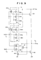
- Fig. 9 diagrammatically shows a BiCMOS logic circuit of a fifth embodiment according to the present invention.
- the circuit in this embodiment includes a first CMOS logic circuit 1 a formed by a pair of PMOSs 33a, 34a and a pair of NMOSs 35a, 36a and a second CMOS circuit 1 b formed by a pair of PMOSs 33b, 34b and a pair of NMOSs 35b, 36b.
- These logic circuits 1a a and 1 have the same configuration, each with the two-input NAND type circuit.
- the difference in this embodiment compared with the third embodiment explained above is that, whereas the NPN bipolar transistor 39, the NMOS 40 and the PMOS 41 are all driven by the CMOS logic circuit 1 in the third embodiment, the first CMOS logic circuit 1a is exclusively for driving the base of the NPN bipolar transistor 39 and the second CMOS logic circuit 1 b is exclusively for driving the gates of the NMOS 40 and the PMOS 41 in the present embodiment.
- the arrangements and operation in other respects are the same as in the third embodiment shown in Fig. 6.
- the output load capacitance to be driven by the first CMOS logic circuit 1a is only the base capacitance of the NPN bipolar transistor 39 and also the output load capacitance to be driven by the second CMOS logic circuit 1 b is only the gate capacitances of the NMOS 40 and the PMOS 41, which can improve speeds of the CMOS logic circuits 1a, 1 thereby enabling the entire circuit to operate at a high speed and enabling the design of MOS circuits to be given more freedom.
- FIG. 10 a sixth embodiment of the present invention is shown in Fig. 10.
- the present invention can provide a BiCMOS circuit which is capable of operating at a high speed even under a low power supply voltage in the order of 3.3 V.
Landscapes
- Engineering & Computer Science (AREA)
- Physics & Mathematics (AREA)
- Computer Hardware Design (AREA)
- Computing Systems (AREA)
- General Engineering & Computer Science (AREA)
- Mathematical Physics (AREA)
- Power Engineering (AREA)
- Logic Circuits (AREA)
Applications Claiming Priority (4)
| Application Number | Priority Date | Filing Date | Title |
|---|---|---|---|
| JP02228687A JP3099351B2 (ja) | 1990-08-29 | 1990-08-29 | BiCMOS論理回路 |
| JP2228691A JPH04109666A (ja) | 1990-08-29 | 1990-08-29 | BiCMOS論理回路 |
| JP228687/90 | 1990-08-29 | ||
| JP228691/90 | 1990-08-29 |
Publications (3)
| Publication Number | Publication Date |
|---|---|
| EP0473409A2 true EP0473409A2 (fr) | 1992-03-04 |
| EP0473409A3 EP0473409A3 (en) | 1992-07-01 |
| EP0473409B1 EP0473409B1 (fr) | 1997-07-16 |
Family
ID=26528406
Family Applications (1)
| Application Number | Title | Priority Date | Filing Date |
|---|---|---|---|
| EP91307873A Expired - Lifetime EP0473409B1 (fr) | 1990-08-29 | 1991-08-28 | Circuit logique BiCMOS |
Country Status (3)
| Country | Link |
|---|---|
| US (1) | US5159214A (fr) |
| EP (1) | EP0473409B1 (fr) |
| DE (1) | DE69126832T2 (fr) |
Cited By (1)
| Publication number | Priority date | Publication date | Assignee | Title |
|---|---|---|---|---|
| EP0701327A3 (fr) * | 1994-09-08 | 1996-06-12 | Nec Corp | Logique du type BiCMOS push-pull avec circuit de verrouillage de tension et de relâchement du verrouillage |
Families Citing this family (7)
| Publication number | Priority date | Publication date | Assignee | Title |
|---|---|---|---|---|
| JPH05198755A (ja) * | 1991-08-29 | 1993-08-06 | Mitsubishi Electric Corp | 半導体論理回路 |
| JP2734254B2 (ja) * | 1991-10-15 | 1998-03-30 | 日本電気株式会社 | レベル変換回路 |
| US5331593A (en) * | 1993-03-03 | 1994-07-19 | Micron Semiconductor, Inc. | Read circuit for accessing dynamic random access memories (DRAMS) |
| JP3441152B2 (ja) * | 1994-04-15 | 2003-08-25 | 株式会社東芝 | BiCMOS回路 |
| JP3633061B2 (ja) * | 1995-10-19 | 2005-03-30 | 三菱電機株式会社 | 半導体集積回路装置 |
| US6307404B1 (en) * | 1999-04-28 | 2001-10-23 | Analog Devices, Inc. | Gate structures with reduced propagation-delay variations |
| TW201026159A (en) * | 2008-12-26 | 2010-07-01 | Vanguard Int Semiconduct Corp | Electrostatic discharge protection circuit and integrated circuit utilizing the same |
Family Cites Families (8)
| Publication number | Priority date | Publication date | Assignee | Title |
|---|---|---|---|---|
| JPH0693626B2 (ja) * | 1983-07-25 | 1994-11-16 | 株式会社日立製作所 | 半導体集積回路装置 |
| JPS60125015A (ja) * | 1983-12-12 | 1985-07-04 | Hitachi Ltd | インバ−タ回路 |
| US4616146A (en) * | 1984-09-04 | 1986-10-07 | Motorola, Inc. | BI-CMOS driver circuit |
| US4649295A (en) * | 1986-01-13 | 1987-03-10 | Motorola, Inc. | BIMOS logic gate |
| JPS62221219A (ja) * | 1986-03-22 | 1987-09-29 | Toshiba Corp | 論理回路 |
| JPS6382122A (ja) * | 1986-09-26 | 1988-04-12 | Toshiba Corp | 論理回路 |
| JPH02214219A (ja) * | 1989-02-14 | 1990-08-27 | Nec Corp | バイポーラmos3値出力バッファ |
| JP2865256B2 (ja) * | 1989-03-02 | 1999-03-08 | 株式会社日立製作所 | バイポーラ・mos論理回路 |
-
1991
- 1991-08-28 EP EP91307873A patent/EP0473409B1/fr not_active Expired - Lifetime
- 1991-08-28 DE DE69126832T patent/DE69126832T2/de not_active Expired - Fee Related
- 1991-08-29 US US07/752,071 patent/US5159214A/en not_active Expired - Fee Related
Cited By (1)
| Publication number | Priority date | Publication date | Assignee | Title |
|---|---|---|---|---|
| EP0701327A3 (fr) * | 1994-09-08 | 1996-06-12 | Nec Corp | Logique du type BiCMOS push-pull avec circuit de verrouillage de tension et de relâchement du verrouillage |
Also Published As
| Publication number | Publication date |
|---|---|
| EP0473409A3 (en) | 1992-07-01 |
| EP0473409B1 (fr) | 1997-07-16 |
| US5159214A (en) | 1992-10-27 |
| DE69126832T2 (de) | 1997-11-20 |
| DE69126832D1 (de) | 1997-08-21 |
Similar Documents
| Publication | Publication Date | Title |
|---|---|---|
| US4779013A (en) | Slew-rate limited output driver having reduced switching noise | |
| US4577124A (en) | CMOS Logic circuit | |
| JP3702159B2 (ja) | 半導体集積回路装置 | |
| US20010017554A1 (en) | Output buffer circuit | |
| EP0351820B1 (fr) | Circuit de sortie | |
| KR910006513B1 (ko) | 바이폴라-상보형 금속산화물 반도체 인버터 | |
| EP0196113A2 (fr) | Circuit tampon à trois états | |
| EP0361841B1 (fr) | Circuit logique bicmos | |
| KR900000487B1 (ko) | 논리 게이트 회로 | |
| US5159214A (en) | Bicmos logic circuit | |
| EP0059722B1 (fr) | Circuit logique synchronise a igfet | |
| KR930001439B1 (ko) | BiCMOS용 출력회로 | |
| EP0055073B1 (fr) | Générateurs de signaux d'horloge électroniques | |
| EP0481698A2 (fr) | Circuit à trois états | |
| US4806797A (en) | bi-CMOS buffer cascaded to CMOS driver having PMOS pull-up transistor with threshold voltage greater than VBE of bi-CMOS bipolar pull-up transistor | |
| JP3179059B2 (ja) | バス制御バッファー増幅器 | |
| EP0196616A2 (fr) | Circuit logique | |
| US5095229A (en) | Full-swing bicmos driver | |
| US5077492A (en) | Bicmos circuitry having a combination cmos gate and a bipolar transistor | |
| KR950000352B1 (ko) | 반도체 논리회로 | |
| US4649290A (en) | Pulse generating circuit | |
| JP3099351B2 (ja) | BiCMOS論理回路 | |
| JP2562824B2 (ja) | バイポーラーcmos論理回路 | |
| JP2511044B2 (ja) | 論理回路 | |
| JP2586196B2 (ja) | 出力回路 |
Legal Events
| Date | Code | Title | Description |
|---|---|---|---|
| PUAI | Public reference made under article 153(3) epc to a published international application that has entered the european phase |
Free format text: ORIGINAL CODE: 0009012 |
|
| 17P | Request for examination filed |
Effective date: 19910912 |
|
| AK | Designated contracting states |
Kind code of ref document: A2 Designated state(s): DE FR GB |
|
| PUAL | Search report despatched |
Free format text: ORIGINAL CODE: 0009013 |
|
| AK | Designated contracting states |
Kind code of ref document: A3 Designated state(s): DE FR GB |
|
| 17Q | First examination report despatched |
Effective date: 19960209 |
|
| GRAG | Despatch of communication of intention to grant |
Free format text: ORIGINAL CODE: EPIDOS AGRA |
|
| GRAH | Despatch of communication of intention to grant a patent |
Free format text: ORIGINAL CODE: EPIDOS IGRA |
|
| GRAH | Despatch of communication of intention to grant a patent |
Free format text: ORIGINAL CODE: EPIDOS IGRA |
|
| GRAA | (expected) grant |
Free format text: ORIGINAL CODE: 0009210 |
|
| AK | Designated contracting states |
Kind code of ref document: B1 Designated state(s): DE FR GB |
|
| REF | Corresponds to: |
Ref document number: 69126832 Country of ref document: DE Date of ref document: 19970821 |
|
| ET | Fr: translation filed | ||
| PLBE | No opposition filed within time limit |
Free format text: ORIGINAL CODE: 0009261 |
|
| STAA | Information on the status of an ep patent application or granted ep patent |
Free format text: STATUS: NO OPPOSITION FILED WITHIN TIME LIMIT |
|
| 26N | No opposition filed | ||
| PGFP | Annual fee paid to national office [announced via postgrant information from national office to epo] |
Ref country code: FR Payment date: 20010810 Year of fee payment: 11 |
|
| PGFP | Annual fee paid to national office [announced via postgrant information from national office to epo] |
Ref country code: GB Payment date: 20010822 Year of fee payment: 11 |
|
| REG | Reference to a national code |
Ref country code: GB Ref legal event code: IF02 |
|
| PG25 | Lapsed in a contracting state [announced via postgrant information from national office to epo] |
Ref country code: GB Free format text: LAPSE BECAUSE OF NON-PAYMENT OF DUE FEES Effective date: 20020828 |
|
| PGFP | Annual fee paid to national office [announced via postgrant information from national office to epo] |
Ref country code: DE Payment date: 20020904 Year of fee payment: 12 |
|
| GBPC | Gb: european patent ceased through non-payment of renewal fee |
Effective date: 20020828 |
|
| PG25 | Lapsed in a contracting state [announced via postgrant information from national office to epo] |
Ref country code: FR Free format text: LAPSE BECAUSE OF NON-PAYMENT OF DUE FEES Effective date: 20030430 |
|
| REG | Reference to a national code |
Ref country code: FR Ref legal event code: ST |
|
| PG25 | Lapsed in a contracting state [announced via postgrant information from national office to epo] |
Ref country code: DE Free format text: LAPSE BECAUSE OF NON-PAYMENT OF DUE FEES Effective date: 20040302 |