EP0474349A2 - Anordnung von Solarzellen - Google Patents
Anordnung von Solarzellen Download PDFInfo
- Publication number
- EP0474349A2 EP0474349A2 EP91306558A EP91306558A EP0474349A2 EP 0474349 A2 EP0474349 A2 EP 0474349A2 EP 91306558 A EP91306558 A EP 91306558A EP 91306558 A EP91306558 A EP 91306558A EP 0474349 A2 EP0474349 A2 EP 0474349A2
- Authority
- EP
- European Patent Office
- Prior art keywords
- solar cell
- support
- cells
- arrangement
- solar
- Prior art date
- Legal status (The legal status is an assumption and is not a legal conclusion. Google has not performed a legal analysis and makes no representation as to the accuracy of the status listed.)
- Ceased
Links
Images



Classifications
-
- H—ELECTRICITY
- H10—SEMICONDUCTOR DEVICES; ELECTRIC SOLID-STATE DEVICES NOT OTHERWISE PROVIDED FOR
- H10F—INORGANIC SEMICONDUCTOR DEVICES SENSITIVE TO INFRARED RADIATION, LIGHT, ELECTROMAGNETIC RADIATION OF SHORTER WAVELENGTH OR CORPUSCULAR RADIATION
- H10F77/00—Constructional details of devices covered by this subclass
- H10F77/40—Optical elements or arrangements
- H10F77/42—Optical elements or arrangements directly associated or integrated with photovoltaic cells, e.g. light-reflecting means or light-concentrating means
- H10F77/488—Reflecting light-concentrating means, e.g. parabolic mirrors or concentrators using total internal reflection
-
- B—PERFORMING OPERATIONS; TRANSPORTING
- B64—AIRCRAFT; AVIATION; COSMONAUTICS
- B64G—COSMONAUTICS; VEHICLES OR EQUIPMENT THEREFOR
- B64G1/00—Cosmonautic vehicles
- B64G1/22—Parts of, or equipment specially adapted for fitting in or to, cosmonautic vehicles
- B64G1/42—Arrangements or adaptations of power supply systems
- B64G1/44—Arrangements or adaptations of power supply systems using radiation, e.g. deployable solar arrays
- B64G1/443—Photovoltaic cell arrays
-
- H—ELECTRICITY
- H10—SEMICONDUCTOR DEVICES; ELECTRIC SOLID-STATE DEVICES NOT OTHERWISE PROVIDED FOR
- H10F—INORGANIC SEMICONDUCTOR DEVICES SENSITIVE TO INFRARED RADIATION, LIGHT, ELECTROMAGNETIC RADIATION OF SHORTER WAVELENGTH OR CORPUSCULAR RADIATION
- H10F19/00—Integrated devices, or assemblies of multiple devices, comprising at least one photovoltaic cell covered by group H10F10/00, e.g. photovoltaic modules
- H10F19/80—Encapsulations or containers for integrated devices, or assemblies of multiple devices, having photovoltaic cells
- H10F19/807—Double-glass encapsulation, e.g. photovoltaic cells arranged between front and rear glass sheets
-
- H—ELECTRICITY
- H10—SEMICONDUCTOR DEVICES; ELECTRIC SOLID-STATE DEVICES NOT OTHERWISE PROVIDED FOR
- H10F—INORGANIC SEMICONDUCTOR DEVICES SENSITIVE TO INFRARED RADIATION, LIGHT, ELECTROMAGNETIC RADIATION OF SHORTER WAVELENGTH OR CORPUSCULAR RADIATION
- H10F19/00—Integrated devices, or assemblies of multiple devices, comprising at least one photovoltaic cell covered by group H10F10/00, e.g. photovoltaic modules
- H10F19/90—Structures for connecting between photovoltaic cells, e.g. interconnections or insulating spacers
- H10F19/902—Structures for connecting between photovoltaic cells, e.g. interconnections or insulating spacers for series or parallel connection of photovoltaic cells
-
- H—ELECTRICITY
- H10—SEMICONDUCTOR DEVICES; ELECTRIC SOLID-STATE DEVICES NOT OTHERWISE PROVIDED FOR
- H10F—INORGANIC SEMICONDUCTOR DEVICES SENSITIVE TO INFRARED RADIATION, LIGHT, ELECTROMAGNETIC RADIATION OF SHORTER WAVELENGTH OR CORPUSCULAR RADIATION
- H10F19/00—Integrated devices, or assemblies of multiple devices, comprising at least one photovoltaic cell covered by group H10F10/00, e.g. photovoltaic modules
- H10F19/90—Structures for connecting between photovoltaic cells, e.g. interconnections or insulating spacers
- H10F19/902—Structures for connecting between photovoltaic cells, e.g. interconnections or insulating spacers for series or parallel connection of photovoltaic cells
- H10F19/904—Structures for connecting between photovoltaic cells, e.g. interconnections or insulating spacers for series or parallel connection of photovoltaic cells characterised by the shapes of the structures
-
- Y—GENERAL TAGGING OF NEW TECHNOLOGICAL DEVELOPMENTS; GENERAL TAGGING OF CROSS-SECTIONAL TECHNOLOGIES SPANNING OVER SEVERAL SECTIONS OF THE IPC; TECHNICAL SUBJECTS COVERED BY FORMER USPC CROSS-REFERENCE ART COLLECTIONS [XRACs] AND DIGESTS
- Y02—TECHNOLOGIES OR APPLICATIONS FOR MITIGATION OR ADAPTATION AGAINST CLIMATE CHANGE
- Y02E—REDUCTION OF GREENHOUSE GAS [GHG] EMISSIONS, RELATED TO ENERGY GENERATION, TRANSMISSION OR DISTRIBUTION
- Y02E10/00—Energy generation through renewable energy sources
- Y02E10/50—Photovoltaic [PV] energy
- Y02E10/52—PV systems with concentrators
Definitions
- This invention relates to solar cell arrangements.
- Solar cells are semi-conductor devices used to convert light into electricity. They usually comprise n and p type semi-conductor layers forming a junction.
- a section through a typical solar cell is shown in Figure 1.
- the solar cell comprises a substrate 1 with a back contact 2 of metal deposited by a vacuum deposition technique. The p and n layers are laid down on the substrate, which supports them, to form a junction 3.
- a conductive layer 4 is formed on the upper surface of the p layer and selectively etched and the exposed p layer metallised to produce a contact grid 5.
- a coverglass 6 protects the cell from dust, abrasion and particle irradiation, and is glued into position by adhesive 7. Connections 8 and 9 are made to the grid 5 and rear metallisation 2.
- a typical solar cell arrangement as shown in Figure 2 includes a plurality of solar cells two of which are shown glued to a cover plate and electrically interconnected by an interconnect 10. Similar interconnects form the electrical connection means throughout the arrangement and it is usual to connect the cells in series. A number of arrangements are mounted together to form solar panels having a large surface area and hence a large collective power output.
- the cycle range is from - 100°C to + 80°C.
- the change in temperature accordingly causes expansion or contraction of the interconnects, the effect of which, over a number of cycles, is to fatigue the links.
- the possible resultant breakage of even one link can be serious, for, in a series arrangement, a large section of the solar panel may fail as a result.
- a solar cell arrangement comprising: a support having at least one recess therein; at least one solar cell directly bonded to the support and at least partially covering the recess and electrical connection means located within the recess and connected to at least one of the layers of the covering portion of the solar cell.
- the electrical connections may be made to the solar cell in such a manner that the connections do not add to the thickness of the arrangement and are flush with the cover plate surface.
- a direct bond that is, a bond not requiring an adhesive can then be made by, for example, heating the support and pressing the solar cell into intimate contact with it. Because the connections are flush with the surface, this avoids areas of high localised stress which would otherwise occur and cause fractures in the semiconductor material.
- the electrical connection means is at least partly a metallisation layer.
- the support is a coverglass. Whilst the coverglass is usually made of glass it may be possible to make it from other materials, for example, plastics and coverglass should be interpreted accordingly.
- a second coverglass is bonded to the back of an arrangement in accordance with the invention as previously described.
- the arrangement has a plurality of interconnected solar cells and a plurality of recesses in the support, the cells being electrically interconnected by the electrical connection means at least partially within the recess.
- a plurality of solar cells so linked would provide a combined power output.
- a second support is provided bonded to the rear of the solar cells bonded to the first support, the cells being electrically interconnected by electrical connection means located in the recesses of the supports.
- the electrical connection means may be arranged to connect layers of adjacent cells such that the front layer of one cell is connected to the rear layer of the adjacent cell.
- the means might be arranged to connect the front layer of one cell to the front layer of its adjacent cell by means in the recesses of one of the supports and the rear layers being similarly connected by means in the recesses of the second plate.
- a reflector is provided to reflect radiation to at least one surface of the solar cell or cells. This will allow the power output to be potentially doubled because both surfaces may be utilised. Since both surfaces may be utilised, each cell will receive the same amount of radiation so avoiding current inequalities due to the differing spectral responses of p and n surfaces which reduce an array's efficiency when only one set of surfaces of the cells in an array are illuminated.
- the reflector reflects radiation to both surfaces of the solar cell or cells. This allows radiation to be gathered over a large area and then "concentrated" over the solar cell surface area making the greatest use of the cell. Further concentration can be conveniently achieved by a parabolic reflector which focuses radiation onto both sides.
- both supports may be transparent to allow the radiation to pass through the rear support.
- the reflector may be a manmade reflector or in some circumstances a celestial body such as the Earth.
- a method of making a solar cell arrangement comprising recessing at least one portion of a support; providing an electrically conductive layer within the recess; and directly bonding a solar cell to the support.
- the support which may be a protective glass coverglass, and making the electrical connection at this region, it is possible to make an intimate bond between the support and the solar cell without the requirement for adhesive, as the face of the solar cell can be flush with the face of the support with any projections on the cell located within the recess or recesses.
- the recess may be made by selectively etching the support or by grinding, for example.
- the electrically conductive layer is a metal deposited by a vacuum deposition technique. Whilst this is preferable, it may also be possible to provide the layer by painting, printing the recess with an electrically conductive ink which dries to form a layer, by insertion in the recess of a metal link or by some other way.
- thinning the solar cell is carried out after bonding.
- Thinning after bonding is advantageous because the solar cell can be made thick enough to be easily handled and bonded to the support without damage and then subsequently thinned.
- the thinning process reduces the weight of the arrangement.
- the thinning is carried out by chemical means such as etching the solar cell. It may also be possible to carry out the thinning process by other means such as mechanical means, for instance grinding the cell.
- a plurality of recesses are made in the support and a plurality of solar cells are positioned such that the recesses are adjacent to electrical connection means on the solar cells prior to bonding.
- the electrical connection means may be a metallised grid made on the solar cell surface for making electrical contact with for instance, the p layer which may project from the surface.
- more than one solar cell is bonded to the support and the cells electrically interconnected by the electrically conducting layer.
- the electrical connections may be achieved by purely physical contact, preferably, the interconnections are fused together. This might be achieved by transmitting energy from a laser, for instance, through the support to selectively melt and fuse the connections together.
- a rearwards layer of the or each solar cell is provided with a pick-up grid after thinning.
- the solar cell By providing a pick-up grid on a rearwards layer, the solar cell can be illuminated through the support and front face and also through the rearmost surface potentially doubling its power output.
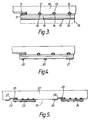
- a single solar cell is produced by etching a glass coverglass 10 to produce recesses 11, 12, 13 and 14.
- the glass coverglass 10 has a thickness in the range of 50 to 500 microns.
- the coverglass is metallised within the recess 11 by a vacuum deposition technique well known to those versed in the art of solar cell manufacture.
- a solar cell 15 is bonded to the coverglass 10 by heating the coverglass, applying an electrostatic potential between the coverglass and solar cell, and pressing the solar cell 15 into contact.
- the solar cell's metallisation layers comprising a grid 16 and a contact pad 17, having a thickness of 5 microns, are aligned with the recesses 12 to 14 and 11 respectively.
- the substrate 18 (shown dotted) is etched away to lighten the solar cell 15 before back metallisation 19 of thickness 5 microns is applied which forms the rear contact of the solar cell 15.
- Front connection to the solar cell 15 is made by fusing the contact pad 17 to the metallisation layer within the recess 12.
- the removal of the substrate allows, in another embodiment, a rear grid to be provided as shown in Figure 4 where after removal of the substrate a back grid 20 and a back contact 21 is produced by metallisation and selective etching.
- the grid 20 allows light from the rear of the cell to pass towards the junction, thereby increasing the cell's output. It is a bifacial solar cell because it has two light sensitive directions as described above.
- Metallisation layers within recesses in the coverglass may be used to link together a number of cells.
- One way in which this may be achieved is by producing a directly bonded, bifacial sub-module as shown in Figure 5, in which a coverglass 22 is etched to provide recesses to accommodate grids of solar cells 23 and 24.
- Recesses 25 and 26 have inclined faces 27 and 28 respectively and are metallised to form metallisation layers 29 and 30.
- the cells 23 and 24 are bonded, etched, metallised and the layers of metallisation fused as before.
- the p layers of the solar cells are uppermost, that is, they are closest to the coverglass 22.
- Another nominally identical sub-module is made as before and then aligned with the other, such that each solar cell of each sub-module is adjacent with a region, such as 31, between the cells of the other sub-module.
- the modules are then glued together with adhesive 32 as shown in Figure 6, a suitable adhesive being Dow Corning 93-500 controlled volatility encapsulant.
- the coverglass metallisation layers are fused as before to interconnect the cells and connect p layers to n layers to form a series arrangement.
- glass coverglasses 33 and 34 with solar cells bonded as before are etched (prior to the bonding of the solar cells) to provide recesses in the regions between the solar cells, 35, 36, 37 and 38. These recesses are provided to accommodate grid electrodes of the solar cells of the other sub-modules.
- the sub-modules After construction of the sub-modules in a similar manner to the embodiments hereinbefore described, they are aligned, re-heated, and pressed together as shown in Figure 8. In this arrangement there is no adhesive required to join the sub-modules since all the bonds are direct bonds.
- Radiation can be reflected onto both faces of the bifacial arrangements described, as shown in Figure 10, where a reflector 42 is formed such that its reflecting surfaces 43 and 44 are orthogonal.
- a bifacial solar cell arrangement 45 which receives radiation reflected from a direction 46 is fixed equidistant between the reflective surfaces 43 and 44.
- a parabolic reflector 47 is used to collect and concentrate radiation onto a bifacial solar cell arrangement 48.
Landscapes
- Engineering & Computer Science (AREA)
- Life Sciences & Earth Sciences (AREA)
- Sustainable Development (AREA)
- Remote Sensing (AREA)
- Aviation & Aerospace Engineering (AREA)
- Photovoltaic Devices (AREA)
Applications Claiming Priority (2)
| Application Number | Priority Date | Filing Date | Title |
|---|---|---|---|
| GB9017982A GB2247564B (en) | 1990-08-16 | 1990-08-16 | A solar cell arrangement |
| GB9017982 | 1990-08-16 |
Publications (2)
| Publication Number | Publication Date |
|---|---|
| EP0474349A2 true EP0474349A2 (de) | 1992-03-11 |
| EP0474349A3 EP0474349A3 (en) | 1992-05-13 |
Family
ID=10680752
Family Applications (1)
| Application Number | Title | Priority Date | Filing Date |
|---|---|---|---|
| EP19910306558 Ceased EP0474349A3 (en) | 1990-08-16 | 1991-07-18 | A solar cell arrangement |
Country Status (3)
| Country | Link |
|---|---|
| EP (1) | EP0474349A3 (de) |
| JP (1) | JPH04233773A (de) |
| GB (1) | GB2247564B (de) |
Cited By (19)
| Publication number | Priority date | Publication date | Assignee | Title |
|---|---|---|---|---|
| DE4427881A1 (de) * | 1994-08-06 | 1996-02-15 | Tnc En Consulting Gmbh | Solarstromanlage |
| EP0786557A1 (de) * | 1996-01-26 | 1997-07-30 | Degussa Aktiengesellschaft | Schallschutzelement für Lärmschutzwände und Verfahren zu dessen Herstellung |
| EP0959506A1 (de) * | 1998-05-19 | 1999-11-24 | Sharp Kabushiki Kaisha | Herstellungsverfahren für dünne Solarzellen |
| EP1030376A1 (de) * | 1999-02-18 | 2000-08-23 | Sharp Kabushiki Kaisha | Solarzellenmodul und Solarzellen-Paneel |
| FR2831714A1 (fr) * | 2001-10-30 | 2003-05-02 | Dgtec | Assemblage de cellules photovoltaiques |
| WO2003038911A1 (fr) * | 2001-10-30 | 2003-05-08 | Solar, Appolon | Assemblage de cellules photovoltaiques et procede de fabrication d'un tel assemblage |
| WO2008112180A3 (en) * | 2007-03-11 | 2009-08-06 | Soliant Energy Inc | Heat transfer and wiring considerations for a photo voltaic receiver for solar concentrator applications |
| US7622666B2 (en) | 2005-06-16 | 2009-11-24 | Soliant Energy Inc. | Photovoltaic concentrator modules and systems having a heat dissipating element located within a volume in which light rays converge from an optical concentrating element towards a photovoltaic receiver |
| WO2009109180A3 (de) * | 2008-03-03 | 2009-12-17 | Fraunhofer-Gesellschaft zur Förderung der angewandten Forschung e.V. | Solarmodul |
| WO2009112544A3 (de) * | 2008-03-14 | 2009-12-23 | Ersol Solar Energy Ag | Verfahren zur herstellung monokristalliner solarzellen mit rückseitiger kontaktstruktur |
| US7688525B2 (en) | 2006-01-17 | 2010-03-30 | Soliant Energy, Inc. | Hybrid primary optical component for optical concentrators |
| WO2011070240A1 (fr) * | 2009-12-09 | 2011-06-16 | Commissariat A L'energie Atomique Et Aux Energies Alternatives | Cellule photovoltaïque, procédé d'assemblage d'une pluralité de cellules et assemblage de plusieurs cellules photovoltaïques |
| CN102437217A (zh) * | 2011-10-14 | 2012-05-02 | 友达光电股份有限公司 | 太阳能电池封装模块 |
| EP2232575A4 (de) * | 2007-12-14 | 2012-07-11 | Miasole | Vor der umwelt geschützte photovoltaikanordnungen |
| WO2012163908A3 (de) * | 2011-06-01 | 2013-03-21 | Schott Solar Ag | Solarzellenmodul und verfahren zum verschalten von solarzellen |
| US8697983B2 (en) | 2008-05-16 | 2014-04-15 | Suncore Photovoltaics, Inc. | Concentrating photovoltaic solar panel |
| CN103650154B (zh) * | 2011-06-01 | 2016-11-30 | 弗劳恩霍弗实用研究促进协会 | 太阳能电池模块和用于太阳能电池的接线的方法 |
| WO2017210570A1 (en) * | 2016-06-03 | 2017-12-07 | Suncore Photovoltaics, Inc. | Solar receiver with cover glass |
| DE102018112104A1 (de) * | 2018-05-18 | 2019-11-21 | Institut Für Solarenergieforschung Gmbh | Laminatfolie und verfahren zum einbetten von solarzellen zur bildung eines photovoltaikmoduls sowie verfahren zum fertigen einer laminatfolie |
Families Citing this family (17)
| Publication number | Priority date | Publication date | Assignee | Title |
|---|---|---|---|---|
| JP2005012241A (ja) * | 2004-09-27 | 2005-01-13 | Sharp Corp | 太陽電池セルの製造方法及び太陽電池セル |
| KR100922710B1 (ko) * | 2009-02-25 | 2009-10-21 | 솔라비토(주) | 태양광 발전장치 및 그 제어방법 |
| DE102011104159A1 (de) * | 2011-06-14 | 2012-12-20 | Institut Für Solarenergieforschung Gmbh | Verfahren zum elektrischen verbinden mehrerer solarzellen und photovoltaikmodul |
| FR2977718B1 (fr) * | 2011-07-07 | 2013-07-12 | Commissariat Energie Atomique | Module photovoltaique a conducteurs sous forme de rubans |
| JP5007894B1 (ja) * | 2011-08-31 | 2012-08-22 | ウーギョン イーエヌジー カンパニー リミテッド | 集光太陽電池モジュール |
| JP2013149794A (ja) * | 2012-01-19 | 2013-08-01 | Toshiyuki Takemura | 太陽光発電装置 |
| WO2014034006A1 (ja) * | 2012-09-03 | 2014-03-06 | 三菱電機株式会社 | 太陽電池素子および太陽電池モジュール |
| US10144533B2 (en) | 2014-05-14 | 2018-12-04 | California Institute Of Technology | Large-scale space-based solar power station: multi-scale modular space power |
| US11128179B2 (en) | 2014-05-14 | 2021-09-21 | California Institute Of Technology | Large-scale space-based solar power station: power transmission using steerable beams |
| WO2015187739A1 (en) | 2014-06-02 | 2015-12-10 | California Institute Of Technology | Large-scale space-based solar power station: efficient power generation tiles |
| US12021162B2 (en) | 2014-06-02 | 2024-06-25 | California Institute Of Technology | Ultralight photovoltaic power generation tiles |
| WO2017015508A1 (en) | 2015-07-22 | 2017-01-26 | California Institute Of Technology | Large-area structures for compact packaging |
| US10454565B2 (en) | 2015-08-10 | 2019-10-22 | California Institute Of Technology | Systems and methods for performing shape estimation using sun sensors in large-scale space-based solar power stations |
| US10992253B2 (en) * | 2015-08-10 | 2021-04-27 | California Institute Of Technology | Compactable power generation arrays |
| JP6484260B2 (ja) * | 2017-01-13 | 2019-03-13 | 株式会社豊田自動織機 | 太陽電池モジュールおよびその製造方法 |
| US11634240B2 (en) | 2018-07-17 | 2023-04-25 | California Institute Of Technology | Coilable thin-walled longerons and coilable structures implementing longerons and methods for their manufacture and coiling |
| US11772826B2 (en) | 2018-10-31 | 2023-10-03 | California Institute Of Technology | Actively controlled spacecraft deployment mechanism |
Family Cites Families (4)
| Publication number | Priority date | Publication date | Assignee | Title |
|---|---|---|---|---|
| US3278811A (en) * | 1960-10-04 | 1966-10-11 | Hayakawa Denki Kogyo Kabushiki | Radiation energy transducing device |
| US3446676A (en) * | 1966-09-07 | 1969-05-27 | Webb James E | Solar battery with interconnecting means for plural cells |
| GB1554507A (en) * | 1977-04-28 | 1979-10-24 | Tideland Signal Corp | Enclosure for solar cells |
| US4554038A (en) * | 1980-08-29 | 1985-11-19 | Trw Inc. | Process for fabricating lightweight, rigid solar array substrate |
-
1990
- 1990-08-16 GB GB9017982A patent/GB2247564B/en not_active Expired - Fee Related
-
1991
- 1991-07-18 EP EP19910306558 patent/EP0474349A3/en not_active Ceased
- 1991-08-16 JP JP3205955A patent/JPH04233773A/ja not_active Withdrawn
Cited By (27)
| Publication number | Priority date | Publication date | Assignee | Title |
|---|---|---|---|---|
| WO1996005622A1 (de) * | 1994-08-06 | 1996-02-22 | Tnc Energie-Consulting Gmbh | Solarstromanlage |
| DE4427881A1 (de) * | 1994-08-06 | 1996-02-15 | Tnc En Consulting Gmbh | Solarstromanlage |
| EP0786557A1 (de) * | 1996-01-26 | 1997-07-30 | Degussa Aktiengesellschaft | Schallschutzelement für Lärmschutzwände und Verfahren zu dessen Herstellung |
| US6184056B1 (en) | 1998-05-19 | 2001-02-06 | Sharp Kabushiki Kaisha | Process for producing solar cells and solar cells produced thereby |
| EP0959506A1 (de) * | 1998-05-19 | 1999-11-24 | Sharp Kabushiki Kaisha | Herstellungsverfahren für dünne Solarzellen |
| US6262358B1 (en) | 1999-02-18 | 2001-07-17 | Sharp Kabushiki Kaisha | Solar cell module and solar cell panel using the same |
| EP1030376A1 (de) * | 1999-02-18 | 2000-08-23 | Sharp Kabushiki Kaisha | Solarzellenmodul und Solarzellen-Paneel |
| FR2831714A1 (fr) * | 2001-10-30 | 2003-05-02 | Dgtec | Assemblage de cellules photovoltaiques |
| WO2003038911A1 (fr) * | 2001-10-30 | 2003-05-08 | Solar, Appolon | Assemblage de cellules photovoltaiques et procede de fabrication d'un tel assemblage |
| US7622666B2 (en) | 2005-06-16 | 2009-11-24 | Soliant Energy Inc. | Photovoltaic concentrator modules and systems having a heat dissipating element located within a volume in which light rays converge from an optical concentrating element towards a photovoltaic receiver |
| US7688525B2 (en) | 2006-01-17 | 2010-03-30 | Soliant Energy, Inc. | Hybrid primary optical component for optical concentrators |
| WO2008112180A3 (en) * | 2007-03-11 | 2009-08-06 | Soliant Energy Inc | Heat transfer and wiring considerations for a photo voltaic receiver for solar concentrator applications |
| EP2232575A4 (de) * | 2007-12-14 | 2012-07-11 | Miasole | Vor der umwelt geschützte photovoltaikanordnungen |
| WO2009109180A3 (de) * | 2008-03-03 | 2009-12-17 | Fraunhofer-Gesellschaft zur Förderung der angewandten Forschung e.V. | Solarmodul |
| WO2009112544A3 (de) * | 2008-03-14 | 2009-12-23 | Ersol Solar Energy Ag | Verfahren zur herstellung monokristalliner solarzellen mit rückseitiger kontaktstruktur |
| US8697983B2 (en) | 2008-05-16 | 2014-04-15 | Suncore Photovoltaics, Inc. | Concentrating photovoltaic solar panel |
| WO2011070240A1 (fr) * | 2009-12-09 | 2011-06-16 | Commissariat A L'energie Atomique Et Aux Energies Alternatives | Cellule photovoltaïque, procédé d'assemblage d'une pluralité de cellules et assemblage de plusieurs cellules photovoltaïques |
| US9112079B2 (en) | 2009-12-09 | 2015-08-18 | Commissariat A L'energie Atomique Et Aux Energies Alternatives | Photovoltaic cell, method for assembling plurality of cells and assembly of a plurality of photovoltaic cells |
| US20150318409A1 (en) * | 2009-12-09 | 2015-11-05 | Commissariat A L'energie Atomique Et Aux Energies Alternatives | Assembly for housing wire elements |
| US10707363B2 (en) | 2009-12-09 | 2020-07-07 | Commissarial A L'Energie Atomique Et Aux Energies Alternatives | Assembly for housing wire elements |
| WO2012163908A3 (de) * | 2011-06-01 | 2013-03-21 | Schott Solar Ag | Solarzellenmodul und verfahren zum verschalten von solarzellen |
| CN103650154A (zh) * | 2011-06-01 | 2014-03-19 | 弗劳恩霍弗实用研究促进协会 | 太阳能电池模块和用于太阳能电池的接线的方法 |
| CN103650154B (zh) * | 2011-06-01 | 2016-11-30 | 弗劳恩霍弗实用研究促进协会 | 太阳能电池模块和用于太阳能电池的接线的方法 |
| DE102011055754B4 (de) | 2011-06-01 | 2022-12-29 | Fraunhofer-Gesellschaft zur Förderung der angewandten Forschung e.V. | Solarzellenmodul und Verfahren zum Verschalten von Solarzellen |
| CN102437217A (zh) * | 2011-10-14 | 2012-05-02 | 友达光电股份有限公司 | 太阳能电池封装模块 |
| WO2017210570A1 (en) * | 2016-06-03 | 2017-12-07 | Suncore Photovoltaics, Inc. | Solar receiver with cover glass |
| DE102018112104A1 (de) * | 2018-05-18 | 2019-11-21 | Institut Für Solarenergieforschung Gmbh | Laminatfolie und verfahren zum einbetten von solarzellen zur bildung eines photovoltaikmoduls sowie verfahren zum fertigen einer laminatfolie |
Also Published As
| Publication number | Publication date |
|---|---|
| EP0474349A3 (en) | 1992-05-13 |
| GB9017982D0 (en) | 1990-10-03 |
| GB2247564B (en) | 1995-01-04 |
| GB2247564A (en) | 1992-03-04 |
| JPH04233773A (ja) | 1992-08-21 |
Similar Documents
| Publication | Publication Date | Title |
|---|---|---|
| EP0474349A2 (de) | Anordnung von Solarzellen | |
| JP7081885B2 (ja) | 太陽電池列のための高効率構成 | |
| US6353175B1 (en) | Two-terminal cell-interconnected-circuits using mechanically-stacked photovoltaic cells for line-focus concentrator arrays | |
| US5344497A (en) | Line-focus photovoltaic module using stacked tandem-cells | |
| US5505789A (en) | Line-focus photovoltaic module using solid optical secondaries for improved radiation resistance | |
| CN108604612B (zh) | 太阳能面板 | |
| EP0657948B1 (de) | Photovoltaischer Konzentrationsmodul und Herstellungsverfahren | |
| US6476314B2 (en) | Solar tile and associated method for fabricating the same | |
| US6034322A (en) | Solar cell assembly | |
| US5017243A (en) | Solar cell and a production method therefor | |
| US10741703B2 (en) | Shingled solar cells overlapping along non-linear edges | |
| US5158618A (en) | Photovoltaic cells for converting light energy to electric energy and photoelectric battery | |
| US4879251A (en) | Method of making series-connected, thin-film solar module formed of crystalline silicon | |
| US20140124013A1 (en) | High efficiency configuration for solar cell string | |
| US20080185034A1 (en) | Fly's Eye Lens Short Focal Length Solar Concentrator | |
| US20130118559A1 (en) | Busses for bifacial photovoltaic cells | |
| EP1630875A2 (de) | Mehrschichtige Bodenplatte einer photovoltaischen Vorrichtung mit optischem Konzentrator | |
| KR20080021706A (ko) | 광전지 집중기 디바이스, 이것으로 형성된 광전지 집중기모듈 및, 이것들의 제조 방법 | |
| EP3491674B1 (de) | Schindelförmige, entlang nichtlinearer kanten überlappende solarzellen | |
| WO2025202078A1 (en) | Method of forming a photovoltaic device and the photovoltaic device | |
| US3532551A (en) | Solar cell including second surface mirrors | |
| WO1987001512A1 (en) | High efficiency photovoltaic assembly | |
| CN119815984A (zh) | 光伏组件及其制备方法 | |
| JPH0360186B2 (de) | ||
| US12027636B2 (en) | Protection coating for solar cell wafers |
Legal Events
| Date | Code | Title | Description |
|---|---|---|---|
| PUAI | Public reference made under article 153(3) epc to a published international application that has entered the european phase |
Free format text: ORIGINAL CODE: 0009012 |
|
| AK | Designated contracting states |
Kind code of ref document: A2 Designated state(s): DE FR IT |
|
| PUAL | Search report despatched |
Free format text: ORIGINAL CODE: 0009013 |
|
| AK | Designated contracting states |
Kind code of ref document: A3 Designated state(s): DE FR IT |
|
| 17P | Request for examination filed |
Effective date: 19920504 |
|
| 17Q | First examination report despatched |
Effective date: 19940905 |
|
| STAA | Information on the status of an ep patent application or granted ep patent |
Free format text: STATUS: THE APPLICATION HAS BEEN REFUSED |
|
| 18R | Application refused |
Effective date: 19950226 |