EP0474490A1 - Antennenanordnung - Google Patents
Antennenanordnung Download PDFInfo
- Publication number
- EP0474490A1 EP0474490A1 EP91308133A EP91308133A EP0474490A1 EP 0474490 A1 EP0474490 A1 EP 0474490A1 EP 91308133 A EP91308133 A EP 91308133A EP 91308133 A EP91308133 A EP 91308133A EP 0474490 A1 EP0474490 A1 EP 0474490A1
- Authority
- EP
- European Patent Office
- Prior art keywords
- antenna
- dipole
- monopole
- conductive
- conductive strip
- Prior art date
- Legal status (The legal status is an assumption and is not a legal conclusion. Google has not performed a legal analysis and makes no representation as to the accuracy of the status listed.)
- Granted
Links
- 230000005404 monopole Effects 0.000 claims abstract description 45
- 230000010287 polarization Effects 0.000 claims abstract description 12
- 230000005540 biological transmission Effects 0.000 claims abstract description 11
- 239000004020 conductor Substances 0.000 claims description 20
- 239000003990 capacitor Substances 0.000 claims description 10
- 239000003989 dielectric material Substances 0.000 claims description 4
- 238000000034 method Methods 0.000 claims description 4
- 238000010276 construction Methods 0.000 description 7
- 238000005457 optimization Methods 0.000 description 5
- 238000004891 communication Methods 0.000 description 4
- 230000000694 effects Effects 0.000 description 4
- WABPQHHGFIMREM-BKFZFHPZSA-N lead-212 Chemical compound [212Pb] WABPQHHGFIMREM-BKFZFHPZSA-N 0.000 description 4
- 239000000758 substrate Substances 0.000 description 4
- 230000000712 assembly Effects 0.000 description 3
- 238000000429 assembly Methods 0.000 description 3
- WABPQHHGFIMREM-BJUDXGSMSA-N lead-206 Chemical compound [206Pb] WABPQHHGFIMREM-BJUDXGSMSA-N 0.000 description 3
- 239000011521 glass Substances 0.000 description 2
- RYGMFSIKBFXOCR-UHFFFAOYSA-N Copper Chemical compound [Cu] RYGMFSIKBFXOCR-UHFFFAOYSA-N 0.000 description 1
- 239000004593 Epoxy Substances 0.000 description 1
- 239000004809 Teflon Substances 0.000 description 1
- 229920006362 Teflon® Polymers 0.000 description 1
- 229910052802 copper Inorganic materials 0.000 description 1
- 239000010949 copper Substances 0.000 description 1
- 238000005562 fading Methods 0.000 description 1
- 230000001939 inductive effect Effects 0.000 description 1
- 239000000463 material Substances 0.000 description 1
- 238000001465 metallisation Methods 0.000 description 1
- 239000004033 plastic Substances 0.000 description 1
- 229920003023 plastic Polymers 0.000 description 1
- 230000005855 radiation Effects 0.000 description 1
- 238000009877 rendering Methods 0.000 description 1
- 230000032258 transport Effects 0.000 description 1
Images


Classifications
-
- H—ELECTRICITY
- H01—ELECTRIC ELEMENTS
- H01Q—ANTENNAS, i.e. RADIO AERIALS
- H01Q21/00—Antenna arrays or systems
- H01Q21/24—Combinations of antenna units polarised in different directions for transmitting or receiving circularly and elliptically polarised waves or waves linearly polarised in any direction
-
- H—ELECTRICITY
- H01—ELECTRIC ELEMENTS
- H01Q—ANTENNAS, i.e. RADIO AERIALS
- H01Q9/00—Electrically-short antennas having dimensions not more than twice the operating wavelength and consisting of conductive active radiating elements
- H01Q9/04—Resonant antennas
- H01Q9/0407—Substantially flat resonant element parallel to ground plane, e.g. patch antenna
-
- H—ELECTRICITY
- H04—ELECTRIC COMMUNICATION TECHNIQUE
- H04B—TRANSMISSION
- H04B7/00—Radio transmission systems, i.e. using radiation field
- H04B7/02—Diversity systems; Multi-antenna system, i.e. transmission or reception using multiple antennas
- H04B7/04—Diversity systems; Multi-antenna system, i.e. transmission or reception using multiple antennas using two or more spaced independent antennas
- H04B7/08—Diversity systems; Multi-antenna system, i.e. transmission or reception using multiple antennas using two or more spaced independent antennas at the receiving station
- H04B7/0802—Diversity systems; Multi-antenna system, i.e. transmission or reception using multiple antennas using two or more spaced independent antennas at the receiving station using antenna selection
Definitions
- This invention relates to antenna assemblies for use in radio communication system.
- a suitable frequency band for a radio LAN lies in the 902 to 928 MHz range.
- an antenna assembly including first and second antennas having different polarization directions, characterized by switching means adapted to render said first antenna or said second antenna selectively operative, wherein said switching means is adapted to detune said first antenna when said second antenna is rendered operative.
- an antenna assembly according to the invention can be implemented as a compact construction since the first and second antennas can be closely positioned, with the detuning provision assisting towards maintaining substantial perpendicularity between the antenna polarizations.
- a method of transmitting data frames in a local area network including a plurality of local area network stations, each station including transceiver means adapted to operate on a wireless transmission channel, and first and second antennas having different polarization directions, characterized in that said method includes the steps of: selecting one of said first and second antennas to be used; and detuning the non-selected one of said first and second antennas.
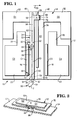
- Fig. 1 is a top view, partially in schematic form, of a first embodiment of an antenna assembly according to the invention.
- Fig. 2 is a perspective view of a cut-away portion of the antenna assembly shown in Fig. 1.
- Fig. 3 is a top view, partially in schematic form, of a first portion of a second embodiment of an antenna assembly according to the invention.
- Fig. 4 is a sectional view of a second portion of the second embodiment of an antenna assembly according to the invention.
- FIG. 1 A first embodiment of an antenna assembly according to the invention will be described with reference to Figs. 1 and 2.
- Fig. 1 there is shown a view of the antenna assembly 10, with certain parts thereof being illustrated only schematically, as an aid to clarity of the drawing.
- the antenna assembly 10 includes a dielectric substrate 12, on which are provided a generally T-shaped conductive area 14, two conductive strips 16 and 18, indicated by references C1 and C3, and two generally rectangular areas 20 and 22, indicated by references C2 and C4, and having extension portions 24 and 26.
- the conductive areas may be formed of copper.
- the T-shaped conductive area 14 includes two generally L-shaped areas 30 and 32, indicated by references D1 and D2, and two strip shaped areas 34 and 36 indicated by references E1 and E2.
- the dashed lines 40, 42, and 44 indicate the boundaries of the conductive areas which abut thereon.
- a dielectric layer 50 (Fig. 2), there is provided a conductive strip 52 having a lower portion 54 (as seen in Fig. 1), a central portion 56 and an upper portion 58.
- the strip portions 54, 56, and 58 are indicated by references G0, G1, and G2 and are bounded by dashed lines 60 and 62.
- the upper strip portion 58 has an interconnection region 64, indicated by reference H, bounded by dashed line 66, which is separated from the plane of the conductive area 14 by the dielectric layer 50, and which is electrically connected to the underlying conductive strip 36 by conductive leads 68, 70, and 72, which extend through the dielectric layer 50.
- a printed circuit board could be used as the substrate for the antenna assembly, with the elements D1, D2, E1, and E2 provided on one side thereof, and the elements C1 to C4, G0 to G2, and H provided on the other side thereof.
- the conductive strip 16 is connected adjacent one end thereof to the conductive strip 54 by a switch 80, also indicated by reference A.
- the strip 16 is also connected, at the other end thereof to the conductive strip 34 by an inductor 82, also indicated by reference L.
- the upper end (as seen in Fig. 1) of the strip portion 56 is connected by a switch 84, also indicated by reference B, and a lead 86 which passes through the dielectric layer 50 (as seen in Fig. 2), with the conductive strip 34.
- the switches 80 and 84 would be implemented as electronic switches.
- a coaxial feed cable 90 also indicated by reference F, has its inner conductor 92 connected to the lower portion 54 of the conductive strip 52 and its outer conductor 94 connected to the strip-shaped area 34 by a conductor 96.
- the antenna assembly 10 implements two antennas having polarization directions which are substantially perpendicular.
- the first antenna is a dipole antenna consisting essentially of the two L-shaped areas 30 and 32, referred to as D1 and D2.
- the second antenna is a monopole antenna consisting essentially of the conductive strip 16, referred to as C1.
- monopole antenna Although referred to as a monopole antenna, it will be appreciated by those skilled in the art that such antenna is effective as a dipole antenna, with the monopole portion (essentially the conductive strip 16 (C1)) serving as one dipole element and the feed cable 90 as the other dipole element.
- the dipole antenna consisting essentially of the (folded) quarter wavelength dipole elements D1 and D2, incorporates a balun (balanced-to-unbalanced) device consisting essentially of the strips E1 and E2 with the strip E1 also serving as the backplane of the microstrip line (G0, G1, G2)/E1, it being remembered that the conductive strip 52 (G0, G1, G2) is connected to the inner conductor 92 of the coaxial cable 90, and the conductive strip 34 (E1) is connected to the outer conductor 94. Also, the conductive area H interconnects the strips G2 and E2 at their upper ends (as seen in Fig.
- a balun device includes an added conductive element (generally, one quarter wavelength) connected to one of the dipole elements, which balances out undesired currents in the conductor feeding the other dipole element.
- the strip line portion G1 is of an electrical length of one-quarter of a wavelength of the relevant radio frequency due to the presence of the dielectric material 50 (dielectric constant greater than 1).
- the physical length of G1 is therefore less than that of the other one-quarter wavelength elements mentioned, namely D1, D2, E1 and E2.
- the physical lengths of the dipole elements D1 and D2 are shown in Fig. 1 as less than the physical lengths of the elements E1, E2.
- the monopole antenna consisting essentially of the conductive strip C1, also includes an impedance matching passive monopole element C2 (conductive area 20), which also radiates, and an inductive element L (shown as coil 82).
- both the dipole antenna (essentially D1, D2) and the monopole antenna (essentially C1) can be used for transmitting or receiving, since any antenna can transmit or receive. Since symmetry and radiation patterns are the same for both directions, the subsequent explanation of the antenna assembly 10 will consider the transmit direction only.
- the dipole antenna (essentially D1 and D2) is in operation.
- the RF energy is provided over the coaxial cable F and transferred over the strip transmission line formed by the strips G0, G1, and G2 and backplane strip E1.
- the upper end of the strip G2 (as seen in Fig. 1) is connected to the extension region H which is connected to the upper end of the strip E2.
- the balun E1 and E2 has a high impedance between its ends for differential-mode.
- the balun also has a high impedance for common-mode, but this mode is substantially not excited by the source, because the microstrip (G0, G1, G2)/E1 transports wave energy to the end at H.
- the dipole D1 and D2 When the dipole D1 and D2 is connected in, the ratio between the common-mode impedances of the dipole (low) and balun (high) results in an even lower common-mode voltage.
- the RF energy is substantially entirely transferred to the dipole in differential-mode, whereby the antenna assembly radiates an E-field in the direction shown by the arrow 100.
- a small amount of energy is transferred to common-mode, but this only slightly affects the polarization.
- the monopole antenna (essentially C1) is in operation.
- the Rf energy applied over the coaxial cable F is transferred via the microstrip line G0/E1 through the switch A to the monopole C1.
- the impedance of the monopole is matched by means of the inductance L (82) and the passive monopole element C2 (20).
- the switch B prevents any RF energy from being transferred to the dipole D1, D2.
- the microstrip G1/E1 does not form a load at the switch A because it is a quarter wavelength microstrip line short-circuited by the switch B. Note that, as discussed hereinabove, the physical length of G1 is less than that of the balun element E1.
- the polarization of the transmitted monopole antenna signal would tend to be disturbed by the presence of the dipole antenna D1 and D2, which acts as a resonator coupled to the monopole antenna. This arises, since, if the dipole antenna D1 and D2 were in tune with the transmitted RF signal, it would pick up RF energy from the monopole antenna, and transmit it with an undesired polarization. According to the present invention, however, the dipole is detuned automatically when the switch B is closed, since the shoft-circuited micfostfip G2/E1 is connected to the dipole, making it resonate at a different frequency, and thus rendering it practically immune to the signals transmitted by the monopole antenna. It will be appreciated that the switch B has three functions: when on, it excludes RF energy from the dipole D1, D2; it creates a high impedance of G1 at the location of the switch A and it detunes the dipole D1 and D2.
- the switches A and B have inherent inductance.
- the inductance of the switch A is accounted for in the impedance matching of the monopole antenna.
- the inductance of the switch B may be tuned out by a series-connected capacitor (not shown in Fig. 1).
- the impedance of the switch B can be arranged to permit a small amount of energy to pass to the dipole antenna, such that a correction signal is transmitted tending to assist in making the polarization of the total transmitted signal approximately perpendicular to that of the dipole.
- the position of the switch B may be varied along the length of the strip 52 to deviate from a quarter wavelength in order to provide a designed impedance at its connection point with the switch A.
- both these effects are taken into account, resulting in a properly matched antenna with maximal difference in polarization between monopole and dipole operation (attainable with these optimization parameters).
- the length of the microstfip G2/E2 can be varied to assist in transmitting a proper correction signal, as well as detuning the dipole.
- the first embodiment was described as being constructed on an insulating substrate, of as a two-sided printed circuit board, it will be appreciated that other constructions are possible for the antenna assembly 10.
- the dipole D1 and D2 and monopole C1 could be formed as fods, while the microstrip line (G0, G1, G2)/E1 could be formed by a coaxial cable.
- the antenna assembly could be constructed from a dielectric (plastics) box having interior metalizations to form the antenna elements.
- FIG. 3 is a top view of the board 202, showing the conductive areas formed thereon, and resistors, capacitors and an inductor indicated schematically but which would be provided as discrete components, mounted on the printed circuit board 202.
- Fig. 4 is a view of the other side of the printed circuit board 202, showing the conductive areas provided thereon, it being appreciated that in the formed antenna assembly 200, Fig. 3 overlies Fig. 4 in the orientation shown with the dielectric material of the board 202 lying between the conductive areas shown in Fig. 3 and 4.
- the letter references for switches A and B, monopole C1, passive monopole C2, passive monopole counterpart C4, dipole D1 and D2, balun E1 and E2, cable F, interconnection H, and inductor L are also utilized in Figs. 2 and 3.
- sufficient symmetry is achieved without the use of a monopole counterpart element C3.
- a coaxial cable 204 (cable F) has its inner conductor connected via a lead 206 which extends from the lower side of the board 202, through a hole (not shown) in a conductive area 208 on the power side of the board 202 to be soldered to a contact area 210 (Fig. 3) provided on the upper side of the board 202.
- the outer conductor of the cable 204 is connected by a lead 212 which extends through a hole (not shown) in the conductive contact area 214, and through the material of the board 202 to contact the conductive area 216 to which the end of the lead 212 is soldered.
- the inner conductor of the cable 204 is electrically connected to the contract area 210, which connects with a generally U-shaped strip 220, forming the strip G0.
- the strip 220 interconnects with a straight strip 222, forming the strip G1.
- switch B The other end of the strip 222 is connected to a switch 234 (switch B) which includes a diode 236 connected to a parallel combination of a resistor 238 and a capacitor 240, which are commonly connected to a contact area 242 which extends through the board 202 to contact a conductive area 244 on the lower side of the board, which connects with a conductive area 246 (balun element E1).
- the contact area 242 is connected to one end of an inductor 248 (inductance L) the other end of which is connected to the monopole conductive area 232.
- the conductive strip 222 is also connected via a capacitor 250 to a conductive strip 252, forming the strip G2, the other end of which connects to a conductive area 250 (interconnection H).
- the conductive area 250 is connected by conductive contact areas 256, 258, and 260, which extend through the board 202 to connect with contact areas 262, 264, and 266 which are connected to a conductive area 268, forming balun element E2.
- the conductive area 246 connects with a conductive area 270, which forms dipole element D1
- the conductive area 268 connects with a conductive area 272 forming dipole element D2.
- a conductive area 274 forms the passive monopole C2
- a conductive area 276 forms the passive monopole counterpart C4.
- switches 224 and 234 are controlled by DC voltages which are applied to the inner conductor of the cable 204, and which are fed via the lead 206 to the contact area 210 (Fig. 3).
- the diodes 226 and 236 are rendered conductive (switches A and B are closed), and the monopole antenna C1 is operative.
- the DC curreat flows via the lead 206, contact area 210, strip 220, diode 226, resistor 228, monopole element C1, coil 248, contact area 242, contact area 244 (Fig. 3) to the balun elemeat E1 and then via contact area 214 and lead 212 back to the outer conductor of the cable 204.
- RF signals are now transferred between element G0 and the monopole element C1.
- the switch 234 (switch B) is rendered conductive, since the diode 236 is forward biased.
- DC current flows from the inner conductor of the cable 204, through the conductive strips G0 and G1, the diode 236, the resistor 238, the contact areas 242 and 244, the conductive element E1, the contact areas 214, 216 and then back via the lead 212 to the outer conductor of the cable 204.
- RF signals passing through microstrip line G1/E1 are substantially short-circuited, yielding a low energy transfer to the dipole D1 and D2 and an almost total reflection of the signal over G1/E1 is the opposite direction, back to switch A.
- the substantially short-circuited microstrip G2/E1 is connected to the dipole D1 and D2, thereby detuning it.
- the capacitor 250 acts as an isolator for DC voltages. For RF signals, it acts as a conductor and/or tuning element, as discussed hereinabove in connection with the opitimization possibilities for the first embodiment. It will also be appreciated that the coil 248 serves to conduct DC to enable the diode 226 to be biased, and also acts as an inductor L for RF signals, thereby assisting in impedence matching for the monopole antenna.
- the antenna assembly 200 when the antenna assembly 200 is utilized in a radio LAN, transmitting is effected only with the dipole antenna to prevent high RF current from damaging the diodes 226, 236. In the receive mode, either antenna may be used.
- antenna assemblies are suitable for use in radio LANs, their use is not restricted thereto, and the antenna assemblies may be employed generally in radio communication systems.
- an epoxy/glass printed circuit board with surface mounted components would be suitable for RF frequency bands between about 500 MHz and 1500 MHz. Above these frequencies teflon/glass may be used up to about 3 GHz. Below these frequencies a physical construction using rods and coaxial cable may be used, rather than a printed circuit board construction.
Landscapes
- Variable-Direction Aerials And Aerial Arrays (AREA)
- Details Of Aerials (AREA)
Applications Claiming Priority (2)
| Application Number | Priority Date | Filing Date | Title |
|---|---|---|---|
| GB909019486A GB9019486D0 (en) | 1990-09-06 | 1990-09-06 | Antenna assembly |
| GB9019486 | 1990-09-06 |
Publications (2)
| Publication Number | Publication Date |
|---|---|
| EP0474490A1 true EP0474490A1 (de) | 1992-03-11 |
| EP0474490B1 EP0474490B1 (de) | 1995-12-06 |
Family
ID=10681778
Family Applications (1)
| Application Number | Title | Priority Date | Filing Date |
|---|---|---|---|
| EP19910308133 Expired - Lifetime EP0474490B1 (de) | 1990-09-06 | 1991-09-05 | Antennenanordnung |
Country Status (3)
| Country | Link |
|---|---|
| EP (1) | EP0474490B1 (de) |
| DE (1) | DE69115177T2 (de) |
| GB (1) | GB9019486D0 (de) |
Cited By (13)
| Publication number | Priority date | Publication date | Assignee | Title |
|---|---|---|---|---|
| GB2295055A (en) * | 1994-11-11 | 1996-05-15 | Plessey Semiconductors Ltd | Conformal antenna for wireless local area network transceivers |
| EP0790662A1 (de) * | 1996-02-14 | 1997-08-20 | Murata Manufacturing Co., Ltd. | Auf einer Oberfläche angeordnete Antenne und dazugehöriges Kommunikationsgerät |
| US6538614B2 (en) | 2001-04-17 | 2003-03-25 | Lucent Technologies Inc. | Broadband antenna structure |
| US7046198B2 (en) | 2001-12-04 | 2006-05-16 | Matsushita Electric Industrial Co., Ltd. | Antenna and apparatus provided with the antenna |
| US7250909B2 (en) | 2003-08-27 | 2007-07-31 | Matsushita Electric Industrial Co., Ltd. | Antenna and method of making the same |
| EP2091103A1 (de) * | 2008-02-15 | 2009-08-19 | Sierra Wireless, Inc. | Kompaktes Diversitätsantennensystem |
| US8090419B2 (en) * | 2004-06-04 | 2012-01-03 | Panasonic Corporation | Folding portable wireless apparatus |
| CN101359770B (zh) * | 2008-09-19 | 2012-06-20 | 清华大学 | 移动终端用的宽带双天线系统 |
| CN104106179A (zh) * | 2012-01-17 | 2014-10-15 | 萨博公司 | 组合天线、天线阵列以及使用该阵列天线的方法 |
| EP2996191A1 (de) * | 2014-09-11 | 2016-03-16 | Neopost Technologies | Planare Antenne für RFID-Lesegerät und RFID-PDA damit |
| CN108429013A (zh) * | 2018-03-13 | 2018-08-21 | 武汉虹信通信技术有限责任公司 | 一种集成rae、sbt和rcu的电调天线控制装置 |
| CN114784513A (zh) * | 2022-06-17 | 2022-07-22 | 微网优联科技(成都)有限公司 | 一种双频高增益单极子天线 |
| CN118589214A (zh) * | 2024-07-12 | 2024-09-03 | 壹通无人机系统有限公司 | 一种方向图可重构的天线结构 |
Families Citing this family (1)
| Publication number | Priority date | Publication date | Assignee | Title |
|---|---|---|---|---|
| CN116264350A (zh) * | 2021-12-15 | 2023-06-16 | 华为技术有限公司 | 天线和电子设备 |
Citations (6)
| Publication number | Priority date | Publication date | Assignee | Title |
|---|---|---|---|---|
| US4379296A (en) * | 1980-10-20 | 1983-04-05 | The United States Of America As Represented By The Secretary Of The Army | Selectable-mode microstrip antenna and selectable-mode microstrip antenna arrays |
| US4538153A (en) * | 1981-09-07 | 1985-08-27 | Nippon Telegraph & Telephone Public Corp. | Directivity diversity communication system with microstrip antenna |
| EP0184383A2 (de) * | 1984-12-06 | 1986-06-11 | AT&T Corp. | Drahtlose Nebenstellenanlage für ein lokales Netzsystem mit optimaler Zusammenfügung |
| GB2176660A (en) * | 1984-05-29 | 1986-12-31 | Licentia Gmbh | Aerial arrangement for electronic proximity fuses or spacing fuses |
| US4800393A (en) * | 1987-08-03 | 1989-01-24 | General Electric Company | Microstrip fed printed dipole with an integral balun and 180 degree phase shift bit |
| EP0318665A2 (de) * | 1987-11-30 | 1989-06-07 | Motorola, Inc. | Steuerschaltung zur Antennenauswahl |
-
1990
- 1990-09-06 GB GB909019486A patent/GB9019486D0/en active Pending
-
1991
- 1991-09-05 DE DE1991615177 patent/DE69115177T2/de not_active Expired - Fee Related
- 1991-09-05 EP EP19910308133 patent/EP0474490B1/de not_active Expired - Lifetime
Patent Citations (6)
| Publication number | Priority date | Publication date | Assignee | Title |
|---|---|---|---|---|
| US4379296A (en) * | 1980-10-20 | 1983-04-05 | The United States Of America As Represented By The Secretary Of The Army | Selectable-mode microstrip antenna and selectable-mode microstrip antenna arrays |
| US4538153A (en) * | 1981-09-07 | 1985-08-27 | Nippon Telegraph & Telephone Public Corp. | Directivity diversity communication system with microstrip antenna |
| GB2176660A (en) * | 1984-05-29 | 1986-12-31 | Licentia Gmbh | Aerial arrangement for electronic proximity fuses or spacing fuses |
| EP0184383A2 (de) * | 1984-12-06 | 1986-06-11 | AT&T Corp. | Drahtlose Nebenstellenanlage für ein lokales Netzsystem mit optimaler Zusammenfügung |
| US4800393A (en) * | 1987-08-03 | 1989-01-24 | General Electric Company | Microstrip fed printed dipole with an integral balun and 180 degree phase shift bit |
| EP0318665A2 (de) * | 1987-11-30 | 1989-06-07 | Motorola, Inc. | Steuerschaltung zur Antennenauswahl |
Cited By (21)
| Publication number | Priority date | Publication date | Assignee | Title |
|---|---|---|---|---|
| GB2295055A (en) * | 1994-11-11 | 1996-05-15 | Plessey Semiconductors Ltd | Conformal antenna for wireless local area network transceivers |
| GB2295055B (en) * | 1994-11-11 | 1998-09-09 | Plessey Semiconductors Ltd | Conformal antenna for wireless local area network transceivers |
| US5821903A (en) * | 1994-11-11 | 1998-10-13 | Plessey Semiconductors Limited | Conformal antenna for wireless local area network transceivers |
| EP0790662A1 (de) * | 1996-02-14 | 1997-08-20 | Murata Manufacturing Co., Ltd. | Auf einer Oberfläche angeordnete Antenne und dazugehöriges Kommunikationsgerät |
| US5867126A (en) * | 1996-02-14 | 1999-02-02 | Murata Mfg. Co. Ltd | Surface-mount-type antenna and communication equipment using same |
| US6538614B2 (en) | 2001-04-17 | 2003-03-25 | Lucent Technologies Inc. | Broadband antenna structure |
| US7046198B2 (en) | 2001-12-04 | 2006-05-16 | Matsushita Electric Industrial Co., Ltd. | Antenna and apparatus provided with the antenna |
| US7250909B2 (en) | 2003-08-27 | 2007-07-31 | Matsushita Electric Industrial Co., Ltd. | Antenna and method of making the same |
| US8090419B2 (en) * | 2004-06-04 | 2012-01-03 | Panasonic Corporation | Folding portable wireless apparatus |
| US7724201B2 (en) | 2008-02-15 | 2010-05-25 | Sierra Wireless, Inc. | Compact diversity antenna system |
| EP2091103A1 (de) * | 2008-02-15 | 2009-08-19 | Sierra Wireless, Inc. | Kompaktes Diversitätsantennensystem |
| CN101359770B (zh) * | 2008-09-19 | 2012-06-20 | 清华大学 | 移动终端用的宽带双天线系统 |
| CN104106179A (zh) * | 2012-01-17 | 2014-10-15 | 萨博公司 | 组合天线、天线阵列以及使用该阵列天线的方法 |
| CN104106179B (zh) * | 2012-01-17 | 2016-05-18 | 萨博公司 | 组合天线、天线阵列以及使用该阵列天线的方法 |
| US9705198B2 (en) | 2012-01-17 | 2017-07-11 | Saab Ab | Combined antenna, antenna array and method for using the antenna array |
| EP2996191A1 (de) * | 2014-09-11 | 2016-03-16 | Neopost Technologies | Planare Antenne für RFID-Lesegerät und RFID-PDA damit |
| US9692129B2 (en) | 2014-09-11 | 2017-06-27 | Neopost Technologies | Planar antenna for RFID reader and RFID PDA incorporating the same |
| CN108429013A (zh) * | 2018-03-13 | 2018-08-21 | 武汉虹信通信技术有限责任公司 | 一种集成rae、sbt和rcu的电调天线控制装置 |
| CN114784513A (zh) * | 2022-06-17 | 2022-07-22 | 微网优联科技(成都)有限公司 | 一种双频高增益单极子天线 |
| CN114784513B (zh) * | 2022-06-17 | 2022-09-13 | 微网优联科技(成都)有限公司 | 一种双频高增益单极子天线 |
| CN118589214A (zh) * | 2024-07-12 | 2024-09-03 | 壹通无人机系统有限公司 | 一种方向图可重构的天线结构 |
Also Published As
| Publication number | Publication date |
|---|---|
| EP0474490B1 (de) | 1995-12-06 |
| GB9019486D0 (en) | 1990-10-24 |
| DE69115177T2 (de) | 1996-07-18 |
| DE69115177D1 (de) | 1996-01-18 |
Similar Documents
| Publication | Publication Date | Title |
|---|---|---|
| US5313218A (en) | Antenna assembly | |
| US6218992B1 (en) | Compact, broadband inverted-F antennas with conductive elements and wireless communicators incorporating same | |
| US6204826B1 (en) | Flat dual frequency band antennas for wireless communicators | |
| EP0944931B1 (de) | Aus vier leitern bestehende wendelantenne für das l-band | |
| EP1590857B1 (de) | Doppelfrequenz-dipolantennenstruktur mit niedrigem profil | |
| EP1055266B1 (de) | Doppelband-diversity-antenne mit parasitärem strahlerelement | |
| EP1506594B1 (de) | Antennenanordnung und modul mit der anordnung | |
| US6198442B1 (en) | Multiple frequency band branch antennas for wireless communicators | |
| EP1031174B1 (de) | Wendelantenne aus vier leitern mit zwei moden und zugehörige verfahren | |
| US6281843B1 (en) | Planar broadband dipole antenna for linearly polarized waves | |
| US5914695A (en) | Omnidirectional dipole antenna | |
| US6229487B1 (en) | Inverted-F antennas having non-linear conductive elements and wireless communicators incorporating the same | |
| US6700543B2 (en) | Antenna element with conductors formed on outer surfaces of device substrate | |
| US20050116869A1 (en) | Multi-band antenna structure | |
| EP0521384A1 (de) | Schichtartig aufgebaute Mehrfachfrequenz-Streifenleiterantenne | |
| EP0474490B1 (de) | Antennenanordnung | |
| WO1998028816A1 (en) | Quadrifilar helix antenna systems and methods for broadband operation in separate transmit and receive frequency bands | |
| US20110128187A1 (en) | Small antenna using srr structure in wireless communication system and method for manufacturing the same | |
| JPH08256009A (ja) | 単一平面プリント回路技術によるモノポール広帯域アンテナおよびそのアンテナを備えた送信及び/又は受信装置 | |
| JP2004266311A (ja) | アンテナ | |
| US20040021605A1 (en) | Multiband antenna for mobile devices | |
| US20020177416A1 (en) | Radio communications device | |
| US10992045B2 (en) | Multi-band planar antenna | |
| GB2289163A (en) | Antenna comprising a closed loop and a ground plane | |
| US5982332A (en) | Broad band transmit and receive antenna |
Legal Events
| Date | Code | Title | Description |
|---|---|---|---|
| PUAI | Public reference made under article 153(3) epc to a published international application that has entered the european phase |
Free format text: ORIGINAL CODE: 0009012 |
|
| AK | Designated contracting states |
Kind code of ref document: A1 Designated state(s): DE FR GB |
|
| 17P | Request for examination filed |
Effective date: 19920831 |
|
| 17Q | First examination report despatched |
Effective date: 19940610 |
|
| RAP1 | Party data changed (applicant data changed or rights of an application transferred) |
Owner name: NCR INTERNATIONAL INC. |
|
| RAP1 | Party data changed (applicant data changed or rights of an application transferred) |
Owner name: AT&T GLOBAL INFORMATION SOLUTIONS INTERNATIONAL IN |
|
| GRAA | (expected) grant |
Free format text: ORIGINAL CODE: 0009210 |
|
| AK | Designated contracting states |
Kind code of ref document: B1 Designated state(s): DE FR GB |
|
| REF | Corresponds to: |
Ref document number: 69115177 Country of ref document: DE Date of ref document: 19960118 |
|
| ET | Fr: translation filed | ||
| PLBE | No opposition filed within time limit |
Free format text: ORIGINAL CODE: 0009261 |
|
| STAA | Information on the status of an ep patent application or granted ep patent |
Free format text: STATUS: NO OPPOSITION FILED WITHIN TIME LIMIT |
|
| 26N | No opposition filed | ||
| REG | Reference to a national code |
Ref country code: FR Ref legal event code: CD |
|
| PG25 | Lapsed in a contracting state [announced via postgrant information from national office to epo] |
Ref country code: DE Effective date: 19970603 |
|
| PG25 | Lapsed in a contracting state [announced via postgrant information from national office to epo] |
Ref country code: FR Effective date: 19970630 |
|
| REG | Reference to a national code |
Ref country code: FR Ref legal event code: ST |
|
| REG | Reference to a national code |
Ref country code: FR Ref legal event code: ST |
|
| REG | Reference to a national code |
Ref country code: GB Ref legal event code: IF02 |
|
| PGFP | Annual fee paid to national office [announced via postgrant information from national office to epo] |
Ref country code: GB Payment date: 20100921 Year of fee payment: 20 |
|
| REG | Reference to a national code |
Ref country code: GB Ref legal event code: PE20 Expiry date: 20110904 |
|
| PG25 | Lapsed in a contracting state [announced via postgrant information from national office to epo] |
Ref country code: GB Free format text: LAPSE BECAUSE OF EXPIRATION OF PROTECTION Effective date: 20110904 |