EP0475199A2 - A fast atom beam source - Google Patents
A fast atom beam source Download PDFInfo
- Publication number
- EP0475199A2 EP0475199A2 EP91114476A EP91114476A EP0475199A2 EP 0475199 A2 EP0475199 A2 EP 0475199A2 EP 91114476 A EP91114476 A EP 91114476A EP 91114476 A EP91114476 A EP 91114476A EP 0475199 A2 EP0475199 A2 EP 0475199A2
- Authority
- EP
- European Patent Office
- Prior art keywords
- electron
- ion
- ion beam
- fast atom
- source
- Prior art date
- Legal status (The legal status is an assumption and is not a legal conclusion. Google has not performed a legal analysis and makes no representation as to the accuracy of the status listed.)
- Granted
Links
Images


Classifications
-
- H—ELECTRICITY
- H05—ELECTRIC TECHNIQUES NOT OTHERWISE PROVIDED FOR
- H05H—PLASMA TECHNIQUE; PRODUCTION OF ACCELERATED ELECTRICALLY-CHARGED PARTICLES OR OF NEUTRONS; PRODUCTION OR ACCELERATION OF NEUTRAL MOLECULAR OR ATOMIC BEAMS
- H05H3/00—Production or acceleration of neutral particle beams, e.g. molecular or atomic beams
- H05H3/02—Molecular or atomic-beam generation, e.g. resonant beam generation
Definitions
- the present invention relates to a fast atom beam source for producing a fast atom beam that is used for sputtering, for example.
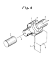
- Fig. 4 shows the arrangement of a fast atom beam source which has heretofore been known.
- reference numeral 1 denotes a hollow, cylindrical casing having a central portion with an enlarged diameter, 2 a circular filament for emitting thermal electrons, 3 an ion beam, 4 a fast atom beam, 5 a power supply for heating the filament 2, 6 a DC bias power supply, and 7 an ion source.
- the circular filament 2 is incorporated in the enlarged-diameter central portion of the casing 1.
- the filament 2 is disposed in such a manner that the center of its circular configuration is coincident with the axis of the casing 1.
- the filament 2 is connected with the heating power supply 5.
- the DC bias power supply 6 is connected between the casing 1 and the filament 2 to bias the casing 1 to a potential which is several V lower than the potential of the filament 2.
- the ion source 7 is disposed so that the ion beam 3 emitted therefrom enters the inside of the casing 1.
- the fast atom beam source thus arranged operates as follows.
- the present invention provides a fast atom beam source comprising: an ion source that emits an ion beam; and an electron gun that emits an electron beam at a speed substantially equal to the speed of the ions in the ion beam emitted from the ion source and in the same direction as that of the ion beam, the electron gun further having the function of mixing the electron beam with the ion beam.
- the electron gun comprises a circular filament which surrounding said ion beam and emits a thermal electron beam and an electron accelerating grid which has a funnel-like configuration arranged such that the ion beam can pass through the central portion thereof and accelerates the electron beam emitted from said circular filament while converting it toward the ion beam.
- the present invention provides a fast atom beam source comprising: an ion source that emits an ion beam; an electron gun that emits an electron beam; speed control means for controlling the speed of the electrons in the electron beam emitted from the electron gun to a level substantially equal to the speed of the ions in the ion beam emitted from the ion source; and means for deflection the electron beam controlled to a predetermined speed by the action of an electric field or a magnetic field so that the electron beam is aligned with the direction of the ion beam and then mixed with it.
- the electron gun emits a thermal electron beam at approximately right angles to said ion beam
- means for deflection comprises a magnet which deflects the electron beam so that said electron beam is aligned with the direction of said ion beam.
- means for deflection comprises two opposing arcuate electrodes which are disposed such that said electron beam is emitted into the area defined therebetween and the surface of the outer arcuate electrode is provided with an ion entrance orifice to allow said ion beam to enter therethrough.
- the electron beam is aligned in the direction of the ion beam and the speed of the electrons in the electron beam is controlled to a level substantially equal to the speed of the ions in the ion beam, the electron beam is mixed with the ion beam, thereby realizing the above-described object of the present invention.
- the electron beam is mixed with the ion beam, thereby reducing the relative velocity between the ions and electrons. In consequence, the recombination cross section of ions and electrons increases, so that the fast atom beam production efficiency is improved.
- Fig. 1 shows a fast atom beam source according to one embodiment of the present invention.
- reference numeral 21 denotes an electron accelerating grid
- 23 an electron beam
- 24 an electron accelerating power supply
- 26 an ion beam entrance orifice provided in a casing 27, and 28 a fast atom beam exit orifice formed in the casing 27 in the same way as in the case of the ion beam entrance orifice 26 at an end of the casing 27 which faces the entrance orifice 26.
- the electron accelerating grid 21 is disposed in the casing 27 in such a manner that it is stretched with an approximately funnel-like configuration, at a position which is forward of the circular filament 2 and at which the accelerating grid 21 faces the exit orifice 28.
- the accelerating grid 21 is arranged such that the ion beam 3 can pass through the central portion thereof and the grid 21 accelerates the electron beam 23 emitted from the circular filament 2 while converging it toward the ion beam 3.
- the electron accelerating power supply 24 is connected between the filament 2 and the electron accelerating grid 21 to bias the grid 21 to a potential which is somewhat higher than that of the filament 2.
- the casing 27 is electrically connected to the electron accelerating grid 21 so as to be equal in potential to the latter.
- the filament 2 and the electron accelerating grid 21 constitute in combination an electron gun.
- the ion beam 3 is emitted from the ion source 7 and enters the casing 7 through the ion entrance orifice 26. At this time, the circular filament 2 is brought to red heat to produce thermal electrons, which are accelerated by the electron accelerating grid 21 to form an electron beam 23.
- the electron beam 23 is converged toward the ion beam 3 entering through the ion entrance orifice 26 by virtue of the above-described configuration of the electron accelerating grid 21.
- the ions in the ion beam 3 recombine with the electrons in the electron beam 23 and return to atoms.
- the ions deliver the kinetic energy to the atoms without a substantial change energitic loss, thus forming a fast atom beam 4 with large kinetic energy, which is then emitted to the outside of the casing 27 through the fast atom beam exit orifice 28.
- the electron accelerating power supply 24 is controlled so that the speed of the electron beam 23 is substantially equal to the speed of the ion beam 3, the recombination cross section between ions and electrons increases, so that the production efficiency of the fast atom beam 4 is improved.
- the red-heat temperature of the filament 2 is controlled so that the number of electrons in the recombination space is sufficiently larger than the number of ions, the fast atom beam production efficiency is further improved.
- Fig. 2 shows another embodiment of the present invention, in which electrons are added to argon ions with an energy of about 10 KeV, for example, thereby producing a fast atom beam of argon.
- reference numeral 31 denotes an electron gun that emits an electron beam 23 at approximately right angles to an ion beam 3 emitted from an ion source 7, 32 a retarding electrode that decelerates electrons, and 33 a retarding power supply that applies a voltage to the retarding electrode 32, the power supply 33 constituting, together with the retarding electrode 32, a speed control means for controlling the speed of the electron beam emitted from the electron gun 31 to a level substantially equal to the speed of the ions in the ion beam 3.
- Reference numeral 34 denotes a magnet serving as a deflection means that deflects the decelerated electron beam 23 so that the electron beam 23 is aligned with the direction of the ion beam 3 and then mixed with it.
- the magnet 34 is disposed at a position where the ion beam 3 emitted from the ion source 7 and the electron beam 34 from the electron gun 31 intersect each other, to apply a magnetic field in a direction normal to the plane of the figure.
- the retarding electrode 32 is disposed in between the electron gun 31 and the magnet 34 at a position which is closer to the magnet 34 from the electron gun 31.
- the electron gun 31 has a conventional structure including a heating filament and an accelerating electrode in a substantially similar manner to that in the foregoing embodiment.
- the mass M of argon ions with an energy of 10 KeV is about 70,000 times the mass m of electrons, if the energy of the electrons is 1/70,000 of the energy of the argon ions, i.e., about 0.14 eV, the argon ions and the electrons are equal in speed to each other.
- electrons that are produced from the electron gun 31 have an energy of several 100 eV or more. It is difficult to produce electrons with an energy below that level directly from the electron gun 31 due to the space-charge effect. Accordingly, it is necessary in order to obtain electrons of 0.14 eV to form an electric field in between the electron gun 31 and the retarding electrode 32 by the retarding power supply 32 to decelerate electrons with a high level of energy (i.e., high speed).
- the electron beam 23 controlled to a predetermined speed enters the magnetic field, which is applied in a direction normal to the plane of the figure by the magnet 34, whereby the orbit of the electron beam 23 is deflected so that the electron beam 23 is aligned with the direction of travel of the ion beam 3, and thereafter the electron beam 23 is mixed with the ion beam 3.
- a fast atom beam 4 of argon is produced.
- Fig. 3 shows still another embodiment of the present invention, in which electrons are added to argon ions with an energy of about 10 KeV to produce a fast atom beam of argon.
- reference numeral 41 denotes an electrostatic deflector for electrons which comprises two opposing arcuate electrodes 41a.
- the surface of the outer arcuate electrode 41 a is provided with an ion entrance orifice 26 to allow an ion beam 3 to enter therethrough.
- the two arcuate electrodes 41 a are disposed such that an electron beam 23 is emitted into the area defined therebetween.
- Reference numeral 42 denotes a deflection power supply that is connected to the electron deflector 41.
- the operation of the fast atom beam source arranged as described above is the same as that of the embodiment shown in Fig. 2 up to the step in which the electron gun 31 produces an electron beam 23 which is substantially equal in speed to argon ions.
- the electron beam 23 enters the electrostatic deflection field that is formed by the electron deflector 41, in which the orbit of the electron beam 23 is deflected so that the electron beam 23 is aligned with the direction of travel of the ion beam 3 by the action of the electric field.
- the argon ion beam 3 passing through the ion entrance orifice 26 is incident on the electron beam 23, thereby producing a fast atom beam 4 of argon.
- ions and electrons are mixed together after their speeds have been equalized with each other, so that the recombination cross section between ions and electrons increases and hence the recombination chance increases, resulting in an improvement in the production efficiency of the fast atom beam.
- the fast atom beam produced in this way can be utilized for the thin film formation by sputtering deposition, the fine pattern processing by sputtering etching, and the material evaluation by secondary ion mass analysis in the same way as in the case of energetic ion beam.
- the fast atom beam since the fast atom beam is chargeless, it can be applied not only to metals and semiconductors but also to insulators such as plastics, ceramics, etc., to which the ion beam technique cannot effectively be applied.
- the present invention which provides a fast atom beam source that emits a fast atom beam efficiently, is very useful for improving the efficiency of processing and analysis.
Landscapes
- Physics & Mathematics (AREA)
- Spectroscopy & Molecular Physics (AREA)
- Engineering & Computer Science (AREA)
- Plasma & Fusion (AREA)
- Electron Sources, Ion Sources (AREA)
- Stabilization Of Oscillater, Synchronisation, Frequency Synthesizers (AREA)
- Analysing Materials By The Use Of Radiation (AREA)
- Particle Accelerators (AREA)
- Physical Deposition Of Substances That Are Components Of Semiconductor Devices (AREA)
- Physical Vapour Deposition (AREA)
Abstract
Description
- The present invention relates to a fast atom beam source for producing a fast atom beam that is used for sputtering, for example.
- Fig. 4 shows the arrangement of a fast atom beam source which has heretofore been known. In the figure,
reference numeral 1 denotes a hollow, cylindrical casing having a central portion with an enlarged diameter, 2 a circular filament for emitting thermal electrons, 3 an ion beam, 4 a fast atom beam, 5 a power supply for heating thefilament 2, 6 a DC bias power supply, and 7 an ion source. - The
circular filament 2 is incorporated in the enlarged-diameter central portion of thecasing 1. Thefilament 2 is disposed in such a manner that the center of its circular configuration is coincident with the axis of thecasing 1. Thefilament 2 is connected with theheating power supply 5. - The DC
bias power supply 6 is connected between thecasing 1 and thefilament 2 to bias thecasing 1 to a potential which is several V lower than the potential of thefilament 2. - The
ion source 7 is disposed so that theion beam 3 emitted therefrom enters the inside of thecasing 1. - It should be noted that the constituent elements, exclusive of the
power supplies - The fast atom beam source thus arranged operates as follows.
- When the
filament 2 is heated by theheating power supply 5, a large number of thermal electrons are emitted therefrom. The thermal electrons are repelled by the wall of thecasing 1 biased to a potential lower than the potential of thefilament 2, so that the thermal electrons concentrate near the axis of thecasing 1, thus forming a high density electron cloud there. When theion beam 3 that is emitted from theion source 7 enters the electron cloud, collision and recombination between ions and electrons occur, so that theion beam 3 is converted into afast atom beam 4. - In the collision between ions and electrons that occur in the above process, since the mass of electrons is much smaller than the mass of ions, the ions deliver the kinetic energy to the atoms without a substantial loss, thus producing a
fast atom beam 4. - However, in the conventional fast atom beam source with the above-described arrangement, the relative velocity between the electrons in the electron cloud and the ions in the ion beam is large and the recombination cross section of ions and electrons is small, so that it is difficult to produce a fast atom beam efficiently.
- In view of the above-described circumstances, it is an object of the present invention to provide a fast atom beam source that produces a fast atom beam efficiently by improving the ion-electron recombination efficiency.
- To attain the above-described object, the present invention provides a fast atom beam source comprising: an ion source that emits an ion beam; and an electron gun that emits an electron beam at a speed substantially equal to the speed of the ions in the ion beam emitted from the ion source and in the same direction as that of the ion beam, the electron gun further having the function of mixing the electron beam with the ion beam. The electron gun comprises a circular filament which surrounding said ion beam and emits a thermal electron beam and an electron accelerating grid which has a funnel-like configuration arranged such that the ion beam can pass through the central portion thereof and accelerates the electron beam emitted from said circular filament while converting it toward the ion beam.
- In addition, the present invention provides a fast atom beam source comprising: an ion source that emits an ion beam; an electron gun that emits an electron beam; speed control means for controlling the speed of the electrons in the electron beam emitted from the electron gun to a level substantially equal to the speed of the ions in the ion beam emitted from the ion source; and means for deflection the electron beam controlled to a predetermined speed by the action of an electric field or a magnetic field so that the electron beam is aligned with the direction of the ion beam and then mixed with it. The electron gun emits a thermal electron beam at approximately right angles to said ion beam, and means for deflection comprises a magnet which deflects the electron beam so that said electron beam is aligned with the direction of said ion beam. means for deflection comprises two opposing arcuate electrodes which are disposed such that said electron beam is emitted into the area defined therebetween and the surface of the outer arcuate electrode is provided with an ion entrance orifice to allow said ion beam to enter therethrough.
- More specifically, after the electron beam is aligned in the direction of the ion beam and the speed of the electrons in the electron beam is controlled to a level substantially equal to the speed of the ions in the ion beam, the electron beam is mixed with the ion beam, thereby realizing the above-described object of the present invention.
- After the electrons are aligned with the direction of the ion beam and the speed of the electrons is controlled to a level substantially equal to the speed of the ions in the ion beam, the electron beam is mixed with the ion beam, thereby reducing the relative velocity between the ions and electrons. In consequence, the recombination cross section of ions and electrons increases, so that the fast atom beam production efficiency is improved.
- Fig. 1 shows the arrangement of a fast atom beam source according to one embodiment of the present invention;
- Fig. 2 shows the arrangement of a fast atom beam source according to another embodiment of the present invention;
- Fig. 3 shows the arrangement of a fast atom beam source according to still another embodiment of the present invention; and
- Fig. 4 shows the arrangement of a fast atom beam source according to a prior art.
- Embodiments of the present invention will be described below with reference to the drawings.
- Fig. 1 shows a fast atom beam source according to one embodiment of the present invention.
- It should be noted that in this embodiment constituent elements having the same functions as those in the prior art described above in connection with Fig. 4 are denoted by the same reference numerals and description thereof is omitted.
- In Fig. 1,
reference numeral 21 denotes an electron accelerating grid, 23 an electron beam, 24 an electron accelerating power supply, 26 an ion beam entrance orifice provided in acasing 27, and 28 a fast atom beam exit orifice formed in thecasing 27 in the same way as in the case of the ionbeam entrance orifice 26 at an end of thecasing 27 which faces theentrance orifice 26. - The
electron accelerating grid 21 is disposed in thecasing 27 in such a manner that it is stretched with an approximately funnel-like configuration, at a position which is forward of thecircular filament 2 and at which the acceleratinggrid 21 faces theexit orifice 28. The acceleratinggrid 21 is arranged such that theion beam 3 can pass through the central portion thereof and thegrid 21 accelerates theelectron beam 23 emitted from thecircular filament 2 while converging it toward theion beam 3. - The electron accelerating
power supply 24 is connected between thefilament 2 and theelectron accelerating grid 21 to bias thegrid 21 to a potential which is somewhat higher than that of thefilament 2. - It should be noted that the
casing 27 is electrically connected to theelectron accelerating grid 21 so as to be equal in potential to the latter. - In this embodiment, the
filament 2 and theelectron accelerating grid 21 constitute in combination an electron gun. - It should be noted that in this embodiment illustration of the above-described filament heating power supply (denoted by
reference numeral 5 in Fig. 4) is omitted for simplification of the drawing. - The operation of the fast atom beam source arranged as described above will next be explained.
- The
ion beam 3 is emitted from theion source 7 and enters thecasing 7 through theion entrance orifice 26. At this time, thecircular filament 2 is brought to red heat to produce thermal electrons, which are accelerated by theelectron accelerating grid 21 to form anelectron beam 23. Theelectron beam 23 is converged toward theion beam 3 entering through theion entrance orifice 26 by virtue of the above-described configuration of theelectron accelerating grid 21. Thus, the ions in theion beam 3 recombine with the electrons in theelectron beam 23 and return to atoms. During the recombination, the ions deliver the kinetic energy to the atoms without a substantial change energitic loss, thus forming afast atom beam 4 with large kinetic energy, which is then emitted to the outside of thecasing 27 through the fast atombeam exit orifice 28. - In the above-described process, if the electron accelerating
power supply 24 is controlled so that the speed of theelectron beam 23 is substantially equal to the speed of theion beam 3, the recombination cross section between ions and electrons increases, so that the production efficiency of thefast atom beam 4 is improved. In addition, if the red-heat temperature of thefilament 2 is controlled so that the number of electrons in the recombination space is sufficiently larger than the number of ions, the fast atom beam production efficiency is further improved. - Fig. 2 shows another embodiment of the present invention, in which electrons are added to argon ions with an energy of about 10 KeV, for example, thereby producing a fast atom beam of argon.
- It should be noted that in this embodiment also constituent elements having the same functions as those in the embodiment described above in connection with Fig. 1 are denoted by the same reference numerals and description thereof is omitted.
- In Fig. 2,
reference numeral 31 denotes an electron gun that emits anelectron beam 23 at approximately right angles to anion beam 3 emitted from anion source 7, 32 a retarding electrode that decelerates electrons, and 33 a retarding power supply that applies a voltage to the retardingelectrode 32, thepower supply 33 constituting, together with the retardingelectrode 32, a speed control means for controlling the speed of the electron beam emitted from theelectron gun 31 to a level substantially equal to the speed of the ions in theion beam 3.Reference numeral 34 denotes a magnet serving as a deflection means that deflects the deceleratedelectron beam 23 so that theelectron beam 23 is aligned with the direction of theion beam 3 and then mixed with it. - The
magnet 34 is disposed at a position where theion beam 3 emitted from theion source 7 and theelectron beam 34 from theelectron gun 31 intersect each other, to apply a magnetic field in a direction normal to the plane of the figure. The retardingelectrode 32 is disposed in between theelectron gun 31 and themagnet 34 at a position which is closer to themagnet 34 from theelectron gun 31. - It should be noted that the
electron gun 31 has a conventional structure including a heating filament and an accelerating electrode in a substantially similar manner to that in the foregoing embodiment. - In addition, the constituent elements, exclusive of the retarding
power supply 33, are accommodated in a vacuum container (not shown). - The operation of this fast atom beam source will next be explained.
- The speed U of ions with a kinetic energy eV1 and a mass M and the speed u of electrons with a kinetic energy eV2 and a mass m are given by


In the present invention, the condition of U = u must be satisfied, and hence, -

- In general, electrons that are produced from the
electron gun 31 have an energy of several 100 eV or more. It is difficult to produce electrons with an energy below that level directly from theelectron gun 31 due to the space-charge effect. Accordingly, it is necessary in order to obtain electrons of 0.14 eV to form an electric field in between theelectron gun 31 and the retardingelectrode 32 by the retardingpower supply 32 to decelerate electrons with a high level of energy (i.e., high speed). - Thus, the
electron beam 23 controlled to a predetermined speed enters the magnetic field, which is applied in a direction normal to the plane of the figure by themagnet 34, whereby the orbit of theelectron beam 23 is deflected so that theelectron beam 23 is aligned with the direction of travel of theion beam 3, and thereafter theelectron beam 23 is mixed with theion beam 3. Thus, afast atom beam 4 of argon is produced. - Fig. 3 shows still another embodiment of the present invention, in which electrons are added to argon ions with an energy of about 10 KeV to produce a fast atom beam of argon.
- It should be noted that in this embodiment constituent elements having the same functions as those in the embodiment described above in connection with Fig. 2 are denoted by the same reference numerals.
- In the figure,
reference numeral 41 denotes an electrostatic deflector for electrons which comprises two opposingarcuate electrodes 41a. The surface of the outerarcuate electrode 41 a is provided with anion entrance orifice 26 to allow anion beam 3 to enter therethrough. The twoarcuate electrodes 41 a are disposed such that anelectron beam 23 is emitted into the area defined therebetween.Reference numeral 42 denotes a deflection power supply that is connected to theelectron deflector 41. - The operation of the fast atom beam source arranged as described above is the same as that of the embodiment shown in Fig. 2 up to the step in which the
electron gun 31 produces anelectron beam 23 which is substantially equal in speed to argon ions. - In this embodiment, the
electron beam 23 enters the electrostatic deflection field that is formed by theelectron deflector 41, in which the orbit of theelectron beam 23 is deflected so that theelectron beam 23 is aligned with the direction of travel of theion beam 3 by the action of the electric field. In this state, theargon ion beam 3 passing through theion entrance orifice 26 is incident on theelectron beam 23, thereby producing afast atom beam 4 of argon. - As has been described above, according to the fast atom beam source of the present invention, ions and electrons are mixed together after their speeds have been equalized with each other, so that the recombination cross section between ions and electrons increases and hence the recombination chance increases, resulting in an improvement in the production efficiency of the fast atom beam.
- The fast atom beam produced in this way can be utilized for the thin film formation by sputtering deposition, the fine pattern processing by sputtering etching, and the material evaluation by secondary ion mass analysis in the same way as in the case of energetic ion beam. In addition, since the fast atom beam is chargeless, it can be applied not only to metals and semiconductors but also to insulators such as plastics, ceramics, etc., to which the ion beam technique cannot effectively be applied. In this sense, the present invention, which provides a fast atom beam source that emits a fast atom beam efficiently, is very useful for improving the efficiency of processing and analysis.
Claims (5)
Applications Claiming Priority (2)
| Application Number | Priority Date | Filing Date | Title |
|---|---|---|---|
| JP226486/90 | 1990-08-30 | ||
| JP2226486A JPH0799720B2 (en) | 1990-08-30 | 1990-08-30 | Fast atom beam source |
Publications (3)
| Publication Number | Publication Date |
|---|---|
| EP0475199A2 true EP0475199A2 (en) | 1992-03-18 |
| EP0475199A3 EP0475199A3 (en) | 1992-07-08 |
| EP0475199B1 EP0475199B1 (en) | 1996-03-27 |
Family
ID=16845858
Family Applications (1)
| Application Number | Title | Priority Date | Filing Date |
|---|---|---|---|
| EP91114476A Expired - Lifetime EP0475199B1 (en) | 1990-08-30 | 1991-08-28 | A fast atom beam source |
Country Status (5)
| Country | Link |
|---|---|
| US (1) | US5221841A (en) |
| EP (1) | EP0475199B1 (en) |
| JP (1) | JPH0799720B2 (en) |
| AT (1) | ATE136192T1 (en) |
| DE (1) | DE69118286T2 (en) |
Cited By (4)
| Publication number | Priority date | Publication date | Assignee | Title |
|---|---|---|---|---|
| US5501613A (en) * | 1993-06-04 | 1996-03-26 | Framatome Connectors International | Connector assembly incorporating superposed connection elements |
| RU2119730C1 (en) * | 1996-12-16 | 1998-09-27 | Институт ядерной физики СО РАН | Source of multicomponent nuclear flows |
| WO1999003125A1 (en) * | 1997-07-10 | 1999-01-21 | Applied Materials, Inc. | Method and apparatus for neutralising space charge in an ion beam |
| US6359286B1 (en) | 1998-07-10 | 2002-03-19 | Applied Materials, Inc. | Method and apparatus for neutralizing space charge in an ion beam |
Families Citing this family (8)
| Publication number | Priority date | Publication date | Assignee | Title |
|---|---|---|---|---|
| JPH05251408A (en) * | 1992-03-06 | 1993-09-28 | Ebara Corp | Etching system |
| US5519213A (en) * | 1993-08-20 | 1996-05-21 | Ebara Corporation | Fast atom beam source |
| US5589685A (en) * | 1995-05-26 | 1996-12-31 | Jen Wu; Kuang | Matrix enhanced SIMS |
| US6835317B2 (en) * | 1997-11-04 | 2004-12-28 | Ebara Corporation | Method of making substrate with micro-protrusions or micro-cavities |
| US6671034B1 (en) * | 1998-04-30 | 2003-12-30 | Ebara Corporation | Microfabrication of pattern imprinting |
| JP3530942B2 (en) * | 2002-03-05 | 2004-05-24 | 独立行政法人通信総合研究所 | Molecular beam generation method and apparatus |
| KR100917010B1 (en) * | 2002-11-27 | 2009-09-10 | 삼성전자주식회사 | Method and apparatus for forming alignment film |
| GB2619948B (en) * | 2022-06-22 | 2024-06-12 | Fusion Reactors Ltd | Neutral beam injection apparatus and method |
Family Cites Families (4)
| Publication number | Priority date | Publication date | Assignee | Title |
|---|---|---|---|---|
| US3846636A (en) * | 1971-08-31 | 1974-11-05 | Reactor Accelerator Dev Int In | Method and means for utilizing accelerated neutral particles |
| US4916311A (en) * | 1987-03-12 | 1990-04-10 | Mitsubishi Denki Kabushiki Kaisha | Ion beaming irradiating apparatus including ion neutralizer |
| US4818872A (en) * | 1987-05-11 | 1989-04-04 | Microbeam Inc. | Integrated charge neutralization and imaging system |
| JPH02100299A (en) * | 1988-10-06 | 1990-04-12 | Nec Corp | High-speed atomic source |
-
1990
- 1990-08-30 JP JP2226486A patent/JPH0799720B2/en not_active Expired - Lifetime
-
1991
- 1991-08-28 EP EP91114476A patent/EP0475199B1/en not_active Expired - Lifetime
- 1991-08-28 AT AT91114476T patent/ATE136192T1/en not_active IP Right Cessation
- 1991-08-28 DE DE69118286T patent/DE69118286T2/en not_active Expired - Fee Related
- 1991-08-30 US US07/752,785 patent/US5221841A/en not_active Expired - Fee Related
Cited By (4)
| Publication number | Priority date | Publication date | Assignee | Title |
|---|---|---|---|---|
| US5501613A (en) * | 1993-06-04 | 1996-03-26 | Framatome Connectors International | Connector assembly incorporating superposed connection elements |
| RU2119730C1 (en) * | 1996-12-16 | 1998-09-27 | Институт ядерной физики СО РАН | Source of multicomponent nuclear flows |
| WO1999003125A1 (en) * | 1997-07-10 | 1999-01-21 | Applied Materials, Inc. | Method and apparatus for neutralising space charge in an ion beam |
| US6359286B1 (en) | 1998-07-10 | 2002-03-19 | Applied Materials, Inc. | Method and apparatus for neutralizing space charge in an ion beam |
Also Published As
| Publication number | Publication date |
|---|---|
| ATE136192T1 (en) | 1996-04-15 |
| DE69118286T2 (en) | 1996-08-29 |
| JPH04109598A (en) | 1992-04-10 |
| EP0475199A3 (en) | 1992-07-08 |
| DE69118286D1 (en) | 1996-05-02 |
| US5221841A (en) | 1993-06-22 |
| EP0475199B1 (en) | 1996-03-27 |
| JPH0799720B2 (en) | 1995-10-25 |
Similar Documents
| Publication | Publication Date | Title |
|---|---|---|
| US4916311A (en) | Ion beaming irradiating apparatus including ion neutralizer | |
| JP2819420B2 (en) | Ion source | |
| EP0475199B1 (en) | A fast atom beam source | |
| US4541890A (en) | Hall ion generator for working surfaces with a low energy high intensity ion beam | |
| US6985553B2 (en) | Ultra-short ion and neutron pulse production | |
| EP0276090A1 (en) | Charge-particle collector | |
| EP0531949B1 (en) | Fast atom beam source | |
| JPH0375975B2 (en) | ||
| US6870320B2 (en) | Device and method for ion beam acceleration and electron beam pulse formation and amplification | |
| EP0058039B1 (en) | Gyrotron device | |
| US4439395A (en) | Neutral beamline with improved ion energy recovery | |
| CA2110067C (en) | Electron accelerator having a coaxial cavity | |
| JP2946433B2 (en) | Ion beam control system | |
| JPH07169425A (en) | Ion source | |
| JPH03194841A (en) | Electron shower | |
| US2758214A (en) | Time-of-flight mass spectrometer | |
| JPS62502023A (en) | energy conversion system | |
| US2931903A (en) | Acceleration and application of high intensity electron beams for radiation processing | |
| JPH0766763B2 (en) | Ion neutralizer | |
| US3912930A (en) | Electron beam focusing system | |
| JPS62112777A (en) | Apparatus for forming thin film | |
| JPH0750637B2 (en) | Fast atom beam source | |
| JPS6347226B2 (en) | ||
| US3525013A (en) | Metallic ion source including plurality of electron guns | |
| JP2671219B2 (en) | Fast atom beam source |
Legal Events
| Date | Code | Title | Description |
|---|---|---|---|
| PUAI | Public reference made under article 153(3) epc to a published international application that has entered the european phase |
Free format text: ORIGINAL CODE: 0009012 |
|
| AK | Designated contracting states |
Kind code of ref document: A2 Designated state(s): AT BE CH DE DK ES FR GB GR IT LI LU NL SE |
|
| PUAL | Search report despatched |
Free format text: ORIGINAL CODE: 0009013 |
|
| AK | Designated contracting states |
Kind code of ref document: A3 Designated state(s): AT BE CH DE DK ES FR GB GR IT LI LU NL SE |
|
| 17P | Request for examination filed |
Effective date: 19930108 |
|
| 17Q | First examination report despatched |
Effective date: 19950515 |
|
| GRAH | Despatch of communication of intention to grant a patent |
Free format text: ORIGINAL CODE: EPIDOS IGRA |
|
| GRAA | (expected) grant |
Free format text: ORIGINAL CODE: 0009210 |
|
| AK | Designated contracting states |
Kind code of ref document: B1 Designated state(s): AT BE CH DE DK ES FR GB GR IT LI LU NL SE |
|
| PG25 | Lapsed in a contracting state [announced via postgrant information from national office to epo] |
Ref country code: IT Free format text: LAPSE BECAUSE OF FAILURE TO SUBMIT A TRANSLATION OF THE DESCRIPTION OR TO PAY THE FEE WITHIN THE PRE;WARNING: LAPSES OF ITALIAN PATENTS WITH EFFECTIVE DATE BEFORE 2007 MAY HAVE OCCURRED AT ANY TIME BEFORE 2007. THE CORRECT EFFECTIVE DATE MAY BE DIFFERENT FROM THE ONE RECORDED.SCRIBED TIME-LIMIT Effective date: 19960327 Ref country code: NL Free format text: LAPSE BECAUSE OF FAILURE TO SUBMIT A TRANSLATION OF THE DESCRIPTION OR TO PAY THE FEE WITHIN THE PRESCRIBED TIME-LIMIT Effective date: 19960327 Ref country code: DK Effective date: 19960327 Ref country code: CH Effective date: 19960327 Ref country code: BE Effective date: 19960327 Ref country code: GR Free format text: LAPSE BECAUSE OF FAILURE TO SUBMIT A TRANSLATION OF THE DESCRIPTION OR TO PAY THE FEE WITHIN THE PRESCRIBED TIME-LIMIT Effective date: 19960327 Ref country code: LI Effective date: 19960327 Ref country code: ES Free format text: THE PATENT HAS BEEN ANNULLED BY A DECISION OF A NATIONAL AUTHORITY Effective date: 19960327 Ref country code: AT Effective date: 19960327 |
|
| REF | Corresponds to: |
Ref document number: 136192 Country of ref document: AT Date of ref document: 19960415 Kind code of ref document: T |
|
| REF | Corresponds to: |
Ref document number: 69118286 Country of ref document: DE Date of ref document: 19960502 |
|
| ET | Fr: translation filed | ||
| PG25 | Lapsed in a contracting state [announced via postgrant information from national office to epo] |
Ref country code: SE Effective date: 19960627 |
|
| PG25 | Lapsed in a contracting state [announced via postgrant information from national office to epo] |
Ref country code: LU Free format text: LAPSE BECAUSE OF NON-PAYMENT OF DUE FEES Effective date: 19960831 |
|
| NLV1 | Nl: lapsed or annulled due to failure to fulfill the requirements of art. 29p and 29m of the patents act | ||
| REG | Reference to a national code |
Ref country code: CH Ref legal event code: PL |
|
| PLBE | No opposition filed within time limit |
Free format text: ORIGINAL CODE: 0009261 |
|
| STAA | Information on the status of an ep patent application or granted ep patent |
Free format text: STATUS: NO OPPOSITION FILED WITHIN TIME LIMIT |
|
| 26N | No opposition filed | ||
| PGFP | Annual fee paid to national office [announced via postgrant information from national office to epo] |
Ref country code: FR Payment date: 20010719 Year of fee payment: 11 |
|
| PGFP | Annual fee paid to national office [announced via postgrant information from national office to epo] |
Ref country code: GB Payment date: 20010814 Year of fee payment: 11 |
|
| PGFP | Annual fee paid to national office [announced via postgrant information from national office to epo] |
Ref country code: DE Payment date: 20010831 Year of fee payment: 11 |
|
| REG | Reference to a national code |
Ref country code: GB Ref legal event code: IF02 |
|
| PG25 | Lapsed in a contracting state [announced via postgrant information from national office to epo] |
Ref country code: GB Free format text: LAPSE BECAUSE OF NON-PAYMENT OF DUE FEES Effective date: 20020828 |
|
| PG25 | Lapsed in a contracting state [announced via postgrant information from national office to epo] |
Ref country code: DE Free format text: LAPSE BECAUSE OF NON-PAYMENT OF DUE FEES Effective date: 20030301 |
|
| GBPC | Gb: european patent ceased through non-payment of renewal fee |
Effective date: 20020828 |
|
| PG25 | Lapsed in a contracting state [announced via postgrant information from national office to epo] |
Ref country code: FR Free format text: LAPSE BECAUSE OF NON-PAYMENT OF DUE FEES Effective date: 20030430 |
|
| REG | Reference to a national code |
Ref country code: FR Ref legal event code: ST |