EP0476389A2 - Verfahren zur Züchtung einer Einkristallhalbleiterverbindung - Google Patents
Verfahren zur Züchtung einer Einkristallhalbleiterverbindung Download PDFInfo
- Publication number
- EP0476389A2 EP0476389A2 EP91114547A EP91114547A EP0476389A2 EP 0476389 A2 EP0476389 A2 EP 0476389A2 EP 91114547 A EP91114547 A EP 91114547A EP 91114547 A EP91114547 A EP 91114547A EP 0476389 A2 EP0476389 A2 EP 0476389A2
- Authority
- EP
- European Patent Office
- Prior art keywords
- crystal
- melt
- temperature
- single crystal
- crucible
- Prior art date
- Legal status (The legal status is an assumption and is not a legal conclusion. Google has not performed a legal analysis and makes no representation as to the accuracy of the status listed.)
- Withdrawn
Links
Images

Classifications
-
- C—CHEMISTRY; METALLURGY
- C30—CRYSTAL GROWTH
- C30B—SINGLE-CRYSTAL GROWTH; UNIDIRECTIONAL SOLIDIFICATION OF EUTECTIC MATERIAL OR UNIDIRECTIONAL DEMIXING OF EUTECTOID MATERIAL; REFINING BY ZONE-MELTING OF MATERIAL; PRODUCTION OF A HOMOGENEOUS POLYCRYSTALLINE MATERIAL WITH DEFINED STRUCTURE; SINGLE CRYSTALS OR HOMOGENEOUS POLYCRYSTALLINE MATERIAL WITH DEFINED STRUCTURE; AFTER-TREATMENT OF SINGLE CRYSTALS OR A HOMOGENEOUS POLYCRYSTALLINE MATERIAL WITH DEFINED STRUCTURE; APPARATUS THEREFOR
- C30B29/00—Single crystals or homogeneous polycrystalline material with defined structure characterised by the material or by their shape
- C30B29/10—Inorganic compounds or compositions
- C30B29/40—AIIIBV compounds wherein A is B, Al, Ga, In or Tl and B is N, P, As, Sb or Bi
-
- C—CHEMISTRY; METALLURGY
- C30—CRYSTAL GROWTH
- C30B—SINGLE-CRYSTAL GROWTH; UNIDIRECTIONAL SOLIDIFICATION OF EUTECTIC MATERIAL OR UNIDIRECTIONAL DEMIXING OF EUTECTOID MATERIAL; REFINING BY ZONE-MELTING OF MATERIAL; PRODUCTION OF A HOMOGENEOUS POLYCRYSTALLINE MATERIAL WITH DEFINED STRUCTURE; SINGLE CRYSTALS OR HOMOGENEOUS POLYCRYSTALLINE MATERIAL WITH DEFINED STRUCTURE; AFTER-TREATMENT OF SINGLE CRYSTALS OR A HOMOGENEOUS POLYCRYSTALLINE MATERIAL WITH DEFINED STRUCTURE; APPARATUS THEREFOR
- C30B15/00—Single-crystal growth by pulling from a melt, e.g. Czochralski method
- C30B15/20—Controlling or regulating
- C30B15/22—Stabilisation or shape controlling of the molten zone near the pulled crystal; Controlling the section of the crystal
-
- C—CHEMISTRY; METALLURGY
- C30—CRYSTAL GROWTH
- C30B—SINGLE-CRYSTAL GROWTH; UNIDIRECTIONAL SOLIDIFICATION OF EUTECTIC MATERIAL OR UNIDIRECTIONAL DEMIXING OF EUTECTOID MATERIAL; REFINING BY ZONE-MELTING OF MATERIAL; PRODUCTION OF A HOMOGENEOUS POLYCRYSTALLINE MATERIAL WITH DEFINED STRUCTURE; SINGLE CRYSTALS OR HOMOGENEOUS POLYCRYSTALLINE MATERIAL WITH DEFINED STRUCTURE; AFTER-TREATMENT OF SINGLE CRYSTALS OR A HOMOGENEOUS POLYCRYSTALLINE MATERIAL WITH DEFINED STRUCTURE; APPARATUS THEREFOR
- C30B29/00—Single crystals or homogeneous polycrystalline material with defined structure characterised by the material or by their shape
- C30B29/10—Inorganic compounds or compositions
- C30B29/46—Sulfur-, selenium- or tellurium-containing compounds
- C30B29/48—AIIBVI compounds wherein A is Zn, Cd or Hg, and B is S, Se or Te
-
- Y—GENERAL TAGGING OF NEW TECHNOLOGICAL DEVELOPMENTS; GENERAL TAGGING OF CROSS-SECTIONAL TECHNOLOGIES SPANNING OVER SEVERAL SECTIONS OF THE IPC; TECHNICAL SUBJECTS COVERED BY FORMER USPC CROSS-REFERENCE ART COLLECTIONS [XRACs] AND DIGESTS
- Y10—TECHNICAL SUBJECTS COVERED BY FORMER USPC
- Y10T—TECHNICAL SUBJECTS COVERED BY FORMER US CLASSIFICATION
- Y10T117/00—Single-crystal, oriented-crystal, and epitaxy growth processes; non-coating apparatus therefor
- Y10T117/10—Apparatus
- Y10T117/1004—Apparatus with means for measuring, testing, or sensing
-
- Y—GENERAL TAGGING OF NEW TECHNOLOGICAL DEVELOPMENTS; GENERAL TAGGING OF CROSS-SECTIONAL TECHNOLOGIES SPANNING OVER SEVERAL SECTIONS OF THE IPC; TECHNICAL SUBJECTS COVERED BY FORMER USPC CROSS-REFERENCE ART COLLECTIONS [XRACs] AND DIGESTS
- Y10—TECHNICAL SUBJECTS COVERED BY FORMER USPC
- Y10T—TECHNICAL SUBJECTS COVERED BY FORMER US CLASSIFICATION
- Y10T117/00—Single-crystal, oriented-crystal, and epitaxy growth processes; non-coating apparatus therefor
- Y10T117/10—Apparatus
- Y10T117/1024—Apparatus for crystallization from liquid or supercritical state
- Y10T117/1032—Seed pulling
Definitions
- the present invention relates to a method of growing single crystal of compound semiconductors having suppressed the generation of twin crystal from the shoulder portion of the single crystal to be pulled up and, in particular, relates to a method of growing single crystal of InP liable to generate the twin crystal.
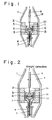
- a heater 3 and a crucible 4 are installed in a hot zone 2 provided in a high-pressure chamber 1 , an inert gas 9 is filled up inside the high pressure chamber 1 , and a melt 13 of raw material of compound semiconductor is retained in the crucible 4 , the top surface of which is covered with a liquid encapsulant 12 .
- a crucible shaft 7 is provided at the lower end of crucible 4 so that the crucible 4 can be rotated and, above the crucible 4 , a rotatable pulling-up shaft 8 attached with a seed crystal 10 at the lower end thereof is provided.
- the invention is characterized in that, in the growing method of single crystal of compound semiconductors by so-called liquid encapsulated Czocharalski method, wherein a melt of raw material of compound semiconductor and a crucible accommodating a liquid encapsulant covering the top surface of said melt are installed in a high-pressure vessel filled up with an inert gas and, after contacting a seed crystal of compound semiconductor with the top surface of the melt of raw material, the seed crystal is pulled upward, thereby gradually solidifying the melt of raw material to grow the single crystal, the crystal is grown on the seed crystal by decreasing the temperature of melt by 6 to 12 °C after dipping the seed crystal into the top surface of the melt of raw material, the temperature at the central portion of melt is first decreased by gradually increasing the rotation of the crucible without drawing up the seed crystal, then, at 0.5 to 2 minutes later, the temperature of melt is further gradually cooled at a lowering rate of -0.21 to -0.88 °C/min to grow the crystal transversely, and, when the
- the invention is characterized in that, upon growing the single crystal of InP by flat top mode using the liquid encapsulated Czocharalski method, the crystal at the beginning of growth is grown laterally in the surface of the melt of InP, then, at the point of time when the size of crystal in the surface of said melt has reached 30 to 40 mm square, the lateral growth is stopped and further, at the point of time when the meniscus at the interface of solid-liquid has become possible to be seen over the whole circumference of the surface of melt, the crystal is pulled up at a pulling-up velocity of not less than 7mm/hr, thereby pulling up the single crystal so as the facet not to appear at the shoulder portion of the crystal.
- Fig. 1 is an outline diagram showing one example of the conventional growing method of the single crystal of compound semiconductor
- Fig. 2 is an illustration diagram of the LEC device used in the example of the invention
- Fig. 3 is an illustration diagram showing how to decrease the melt temperature and the change in the rotation of crucible over time at the start of growing crystal in the invention
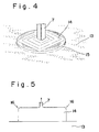
- Fig. 4 is a schematic figure showing the meniscus appearing at the interface of solid-liquid when the diameter of crystal has been stabilized according to the invention
- Fig. 5 is a side view showing the vicinity of the shoulder portion when the crystal was pulled up by flat top according to the invention
- Fig. 1 is an outline diagram showing one example of the conventional growing method of the single crystal of compound semiconductor
- Fig. 2 is an illustration diagram of the LEC device used in the example of the invention
- Fig. 3 is an illustration diagram showing how to decrease the melt temperature and the change in the rotation of crucible over time at the start of growing crystal in the invention
- Fig. 4 is a schematic figure showing the meniscus appearing at the interface
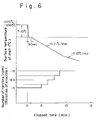
- FIG. 6 is an illustration diagram showing how to decrease the melt temperature and the change in the rotation of crucible over time at the start of growing crystal in one example of the invention
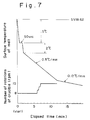
- Fig. 7 is an illustration diagram showing how to decrease the temperature and how to increase the number of rotations of crucible at the start of growing in another example of the invention
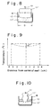
- Fig. 8 is a side cross section showing the state of the crystal of InP pulled up from the crucible according to the invention
- Fig. 9 is a diagram of an approximate distribution of temperature in the horizontal direction of the surface of melt in the invention
- Fig. 10 is a side cross section showing the state of the crystal of InP pulled up conventionally.
- the single crystal is pulled up by, so to speak, flat top shape.
- the tip of the seed crystal is dipped into the melt of raw material by bringing down the seed crystal into the melt of raw material and, first, the growth of crystal is started without pulling up the seed crystal.
- the seed crystal is allowed to rotate at 3 rpm or so.
- the temperature of melt is decreased by 6 to 12 °C, then, at 0.5 to 2 minutes later, the temperature is decreased at a temperature-lowering rate of -0.21 to -0.88 °C/min, thereby the crystal can be grown laterally from the seed crystal. Thereafter, by gradually increasing the number of rotations of crucible, the crystal is made larger further. Since, if increasing the rotation of crucible, the temperature at the central portion of melt is usually decreased, the number of rotations of crucible is changed from -5 rpm to -15 rpm, thereby the temperature at the central portion of melt can be decreased by about 8 °C.
- the crystal is extended laterally, the shape of crystal is brought close to a required shape, the temperature-lowering rate is made as low as -0.15 °C/min, and, when reaching the required diameter (60-65 mm), the seed crystal is pulled upward at a velocity of 10 mm/hr.
- the second aspect of the invention in the growth of compound semiconductor, like InP, single crystal with a diameter of 2 in. by flat top shape using LEC device, InP poly raw material is molten, the tip of seed is dipped into this, and this state is kept for about 15 minutes, then the growth of crystal is started. At this time, under the control of temperature-lowering and number of rotations of crucible, the crystal is grown on the seed and this crystal is grown laterally. When the size of crystal has reached 30 to 40 mm square, the temperature-lowering rate is made to be 0.13 to 0 °C/min to stop the growth of crystal.
- the meniscus concave shape of interface where the melt contacts with the crystal due to interfacial tension
- the pulling-up of the crystal is started.
- the reason why the temperature-lowering rate on stopping the diameter of crystal is in the range of 0.13 to 0 °C/min is that, if the temperature of melt on stopping the diameter of the crystal is settled a little too high, the temperature-lowering rate is increased to prevent the diameter of the crystal from becoming thin after the start of pulling-up. Also, if the temperature of the melt is settled a little too low,the temperature-lowering rate is decreased to come close to 0 °C/min. In this way, by pulling up the crystal at a pulling-up velocity of not less than 7 mm/hr when the shape of meniscus has been stabilized, the pulled-up crystal has no facet at the shoulder portion to give a single crystal.
- InP seed is dipped into the melt after the InP polycrystal in quartz crucible has been molten (Temperature 1070 °C) and the temperature of the melt is decreased stepwise by 7 to 10 °C to make supercooling and to grow the crystal laterally on the seed.
- the crystal has reached a fixed diameter, the crystal is pulled up.
- the crystal when using a crucible with an inner diameter of 65 to 70 mm, the crystal is not pulled up until the diameter of InP crystal reaches 55 to 60 mm and, at the point of time when reaching this diameter, the crystal is pulled up.
- the head portion of the crystal comes out of about 17 mm thick B2O3 being an encapsulant covering the melt and the amount of radiation from the surface of crystal changes, nevertheless it becomes hard to affect the diameter of crystal and the diameter of crystal is easy to be controlled constantly. This is because the lateral distribution of temperature in the melt is maintained so that the temperature is high at the periphery of the crucible and low at the central portion of the melt.
- the means to make the radial distribution of the temperature of the melt so that the temperature is high at the central portion of the melt and low at the peripheral portion as described there is a method of control by the pressure of atmospheric gas, a method of controlling the magnitude of thermal insulation of the device for heating the crucible, and the like. For example, if decreasing the pressure of gas or increasing the efficiency of thermal insulation, said distribution of temperature would tend to become more uniform and, inversely, if increasing the pressure of gas or decreasing the efficiency of thermal insulation, the temperature at the central portion of the melt would become lower.
- the lateral distribution of the melt can always be maintained so that the temperature is higher at the peripheral portion permitting the drawing-up of a crystal of stabilized shape.
- the invention exerts a substantial effect in that, in the pulling-up of the single crystal of compound semiconductors by the LEC method of flat top shape, the shape of crystal can be maintained stably making it possible to pull up the single crystal in good retention.
- Fig. 2 The growth of the single crystal of InP was performed using the LEC device shown in Fig. 2, in which similar parts are designated with the same reference signs as in Fig. 1.
- numeral 1 indicates high-pressure chamber
- numeral 2 indicates hot zone
- numeral 3 indicates heater
- numeral 4 indicates crucible
- numeral 8 indicates pulling-up shaft
- numeral 9 indicates inert gas
- numeral 10 indicates seed
- numeral 12 indicates B2O3
- numeral 13 indicates InP poly raw material
- numeral 7 indicates crucible shaft
- numeral 5 indicates thermocouple
- numeral 6 indicates electrode.
- the InP poly raw material charge weighed 1.2 kg
- B2O3 weighed 200 g, and, as a crucible, quartz crucible with a size of 4 in. was used.
- seed with (001) orientation was used.
- the heater was a wine cup heater
- the inert gas introduced into the high-pressure chamber was Ar or N2, and the pressure of gas was 35 kg/cm2.
- InP poly raw material (9) was molten in the crucible (4)(temperature of melt was about 1070 °C). After melting the InP, the tip of seed (7) was dipped into the melt. After retained in this state for 15 minutes or so, the growth of crystal was started. How to decrease the temperature and the change in the number of rotations of crucible over time at this time is shown in Fig. 3. Namely, the temperature of the melt is first decreased by 8 °C (7 to 10 °C is suitable) to make supercooling and then the crystal is grown. The temperature-lowering rate is given so as this crystal to grow in the shape of square and the number of rotations of crucible is gradually increased.
- the temperature-lowering rate was controlled within 0.13 to 0 °C/min to stop the lateral growth of crystal on the surface of the melt. And, at this time, the number of rotations of the crucible had already been made constant to be -15 rpm.
- the crystal pulled up in this way had flat top shape as shown in Fig. 5 and no facet face appeared at the shoulder portion (16) to give a single crystal (14) hard without incorporation of a twin crystal.
- the temperature-lowering rate is made to be 0 from first as it is and the pulling-up is started when it has been stabilized.
- a temperature-lowering rate of about 0.2 °C/min may be given and the crystal may be pulled up at a velocity of 10 mm/hr or so.
- the growth of the single crystal of InP was performed using the LEC device shown in Fig. 2.
- the InP crystal charge weighed 1.2 kg, B2O3 weighed 200 g, and, as a crucible, quartz crucible with a size of diameter of 4 in. was used.
- the seed crystal of InP was one with (001) orientation and wine cup type heater was used.
- Ar or N2 gas was introduced into the high-pressure chamber and the pressure of gas was made to be 35 kg/cm2.
- the polycrystal raw material of InP was molten, the temperature inside the crucible was made to be 1070 °C (above 1062 °C being a melting temperature of InP), and, after made up the melt of InP, the seed crystal was brought down to dip the tip of the seed crystal into the melt. At 15 minutes later after dipping the seed crystal into the melt (after the temperature of the melt had been stabilized), the growth of crystal was started. How to decrease these temperatures and how to rotate the crucible will be illustrated using Fig. 6. Besides, the number of rotations of the seed crystal is 3 rpm.
- the temperature of the melt is decreased by 7 °C or so and, at 50 seconds later, the temperature of the crucible is decreased at a temperature-lowering rate of -0.21 °C/min, thereby the crystal starts to grow at four corners of the seed crystal.
- the rotation of the crucible is gradually increased.
- the temperature at the central portion is usually decreased and, by changing the rotation of the crucible from -5 rpm to -15 rpm, the temperature of the melt can be decreased by 8 °C or so.
- the temperature-lowering rate is made low (-0.15 °C/min).
- the seed crystal was pulled up at a velocity of 10 mm/hr to grow the crystal.
- the generation of twin or dendrite was suppressed and a good single crystal of InP could be obtained.
- Example 2 the growth of a single crystal of InP was performed. At this time, how to decrease the temperature and how to rotate the crucible are as shown in Fig. 7.
- the rotation of the crucible is often gradually increased from 8 to 15 revolutions.
- the temperature-lowering rate is also made to be -0.5 °C/min being two times as high as in the case of Example 1 aforementioned. If the extending rate of crystal is low, the temperature-lowering rate is made high and preferably is (-1 °C/min ⁇ T/ ⁇ t ⁇ -0.1 °C/min), wherein ⁇ T denotes the variation in the temperature on the surface of the melt and ⁇ t denotes the time during which the temperature is varied.
- This method pulling up the crystal by flat top is very advantageous for the growth of crystal, because, when the head portion has been single-crystallized to the required diameter, it is only necessary to pull up the crystal at a fixed temperatute as it is.
- This method of growing crystal can be applied also to the growth of crystals of other compound semiconductors such as GaAs, GaSb, InSb, InAs etc.
- a crucible 4 with an inner diameter of 66 mm was used and a seed with (001) orientation and a wine cup heater were used for InP seed and heater, respectively.
- a seed with (001) orientation and a wine cup heater were used for InP seed and heater, respectively.
- 35 kg/cm2 of Ar or N2 being an inert gas were introduced into the high-pressure chamber.
- the amount of InP poly raw material is about 1200 g.
- InP poly raw material in quartz crucible was first molten (temperature 1070 °C)
- InP seed was dipped into the melt and the temperature of the melt was decreased stepwise by 7 to 10 °C to produce supercooling, thus growing the crystal laterally on the seed.
- the pulling-up situation of the crystal is shown in Fig. 8.
- numerals 4 , 10, 12, 13' and 11' indicate crucible, seed, B2O3, melt and crystal, respectively and, at the point of time when the diameter of the crystal 11' had reached 60 mm, the crystal 11' was pulled up.
- the pulling-up velocity, the temperature-lowering rate and the thickness of B2O3 were made to be 10 mm/hr, 0.05 °C/min and about 17 mm, respectively.
- a crucible with an inner diameter of to 70 mm is used for pulling up a crystal with a diameter of 55 to 60 mm, as illustrated above.
- a crucible with an inner diameter of 90 to 95 mm may be used and, when pulling up a crystal with a diameter of 105 to 110 mm, a crucible with an inner diameter of 115 to 120 mm may be used, making the distribution of temperature in the melt so that the temperature becomes gradually lower as approaching closer to the central portion of the melt as described above.
Landscapes
- Chemical & Material Sciences (AREA)
- Engineering & Computer Science (AREA)
- Crystallography & Structural Chemistry (AREA)
- Materials Engineering (AREA)
- Metallurgy (AREA)
- Organic Chemistry (AREA)
- Inorganic Chemistry (AREA)
- Crystals, And After-Treatments Of Crystals (AREA)
- Liquid Deposition Of Substances Of Which Semiconductor Devices Are Composed (AREA)
Applications Claiming Priority (6)
| Application Number | Priority Date | Filing Date | Title |
|---|---|---|---|
| JP228822/90 | 1990-08-30 | ||
| JP22882290A JP2834558B2 (ja) | 1990-08-30 | 1990-08-30 | 化合物半導体単結晶の成長方法 |
| JP28144490A JPH04160095A (ja) | 1990-10-19 | 1990-10-19 | 化合物半導体単結晶の成長方法 |
| JP281443/90 | 1990-10-19 | ||
| JP28144390A JPH04160099A (ja) | 1990-10-19 | 1990-10-19 | InP単結晶成長方法 |
| JP281444/90 | 1990-10-19 |
Publications (2)
| Publication Number | Publication Date |
|---|---|
| EP0476389A2 true EP0476389A2 (de) | 1992-03-25 |
| EP0476389A3 EP0476389A3 (en) | 1993-06-09 |
Family
ID=27331439
Family Applications (1)
| Application Number | Title | Priority Date | Filing Date |
|---|---|---|---|
| EP19910114547 Withdrawn EP0476389A3 (en) | 1990-08-30 | 1991-08-29 | Method of growing single crystal of compound semiconductors |
Country Status (2)
| Country | Link |
|---|---|
| US (1) | US5379717A (de) |
| EP (1) | EP0476389A3 (de) |
Cited By (4)
| Publication number | Priority date | Publication date | Assignee | Title |
|---|---|---|---|---|
| US5493985A (en) * | 1993-02-26 | 1996-02-27 | The United States Of America As Represented By The Secretary Of The Air Force | Process and apparatus for controlled synthesis and in-situ single crystal growth of phosphorus compounds and the crystals therefrom |
| GB2305877A (en) * | 1995-10-02 | 1997-04-23 | Gen Electric | Method for providing an extension on an end of an article |
| US6019841A (en) * | 1997-03-24 | 2000-02-01 | G.T. Equuipment Technologies Inc. | Method and apparatus for synthesis and growth of semiconductor crystals |
| US20220081799A1 (en) * | 2019-11-22 | 2022-03-17 | The 13Th Research Institute Of China Electronics Technology Group Corporation | Method for preparing indium phosphide crystal by utilizing indium-phosphorus mixture |
Families Citing this family (3)
| Publication number | Priority date | Publication date | Assignee | Title |
|---|---|---|---|---|
| JP4120777B2 (ja) * | 2002-04-30 | 2008-07-16 | 信越半導体株式会社 | InP単結晶の製造方法及びInP単結晶 |
| TW200528592A (en) * | 2004-02-19 | 2005-09-01 | Komatsu Denshi Kinzoku Kk | Method for manufacturing single crystal semiconductor |
| US8815010B2 (en) * | 2004-04-28 | 2014-08-26 | Nippon Mining & Metals Co., Ltd. | InP single crystal wafer and method for producing InP single crystal |
Family Cites Families (6)
| Publication number | Priority date | Publication date | Assignee | Title |
|---|---|---|---|---|
| US3980438A (en) * | 1975-08-28 | 1976-09-14 | Arthur D. Little, Inc. | Apparatus for forming semiconductor crystals of essentially uniform diameter |
| US4299651A (en) * | 1979-06-11 | 1981-11-10 | Bell Telephone Laboratories, Incorporated | Production of single crystal II-V material |
| JPS60226492A (ja) * | 1984-04-23 | 1985-11-11 | Toshiba Corp | 化合物半導体単結晶の製造装置 |
| JPS60264390A (ja) * | 1984-06-08 | 1985-12-27 | Sumitomo Electric Ind Ltd | 単結晶の育成方法 |
| CA1241902A (en) * | 1987-07-20 | 1988-09-13 | Normand Julien | Supporting device for wheelchairs |
| JPH0774117B2 (ja) * | 1989-10-20 | 1995-08-09 | 信越半導体株式会社 | ヒータの温度パターン作成方法及びこの温度パターンを用いたSi単結晶育成制御装置 |
-
1991
- 1991-08-29 EP EP19910114547 patent/EP0476389A3/en not_active Withdrawn
-
1993
- 1993-05-18 US US08/063,344 patent/US5379717A/en not_active Expired - Fee Related
Cited By (7)
| Publication number | Priority date | Publication date | Assignee | Title |
|---|---|---|---|---|
| US5493985A (en) * | 1993-02-26 | 1996-02-27 | The United States Of America As Represented By The Secretary Of The Air Force | Process and apparatus for controlled synthesis and in-situ single crystal growth of phosphorus compounds and the crystals therefrom |
| GB2305877A (en) * | 1995-10-02 | 1997-04-23 | Gen Electric | Method for providing an extension on an end of an article |
| US5778960A (en) * | 1995-10-02 | 1998-07-14 | General Electric Company | Method for providing an extension on an end of an article |
| GB2305877B (en) * | 1995-10-02 | 1999-12-22 | Gen Electric | Method for providing an extension of an end of an article |
| US6019841A (en) * | 1997-03-24 | 2000-02-01 | G.T. Equuipment Technologies Inc. | Method and apparatus for synthesis and growth of semiconductor crystals |
| US20220081799A1 (en) * | 2019-11-22 | 2022-03-17 | The 13Th Research Institute Of China Electronics Technology Group Corporation | Method for preparing indium phosphide crystal by utilizing indium-phosphorus mixture |
| US11781240B2 (en) * | 2019-11-22 | 2023-10-10 | The 13Th Research Institute Of China Electronics Technology Group Corporation | Method for preparing indium phosphide crystal by utilizing indium-phosphorus mixture |
Also Published As
| Publication number | Publication date |
|---|---|
| EP0476389A3 (en) | 1993-06-09 |
| US5379717A (en) | 1995-01-10 |
Similar Documents
| Publication | Publication Date | Title |
|---|---|---|
| US5607507A (en) | System for oxygen precipitation control in silicon crystals | |
| EP0751242B1 (de) | Kristallwachstumsverfahren | |
| US5342475A (en) | Method of growing single crystal of compound semiconductor | |
| US5379717A (en) | Method of growing single crystal of compound semiconductors | |
| JP3806791B2 (ja) | 化合物半導体単結晶の製造方法 | |
| EP0266227B1 (de) | Verfahren zur Züchtung von Kristallen aus Halbleiterverbindungen | |
| US5820672A (en) | OISF control in czochralski-grown crystals | |
| JP4344021B2 (ja) | InP単結晶の製造方法 | |
| EP0355833B1 (de) | Verfahren zur Herstellung eines Einkristalls aus einer Halbleiter-Verbindung | |
| JP2531875B2 (ja) | 化合物半導体単結晶の製造方法 | |
| JPH05194073A (ja) | 化合物半導体の単結晶成長方法 | |
| JP3885245B2 (ja) | 単結晶引上方法 | |
| JP3018738B2 (ja) | 単結晶製造装置 | |
| JP2834558B2 (ja) | 化合物半導体単結晶の成長方法 | |
| US20250283245A1 (en) | Transparent horizontal gradient freeze apparatus with regulated growth rate | |
| JPH09175892A (ja) | 単結晶の製造方法 | |
| JP2814796B2 (ja) | 単結晶の製造方法及びその装置 | |
| US20030200915A1 (en) | Production method for InP single crystal and InP single crystal | |
| JP2542434B2 (ja) | 化合物半導体結晶の製造方法および製造装置 | |
| JPH03193689A (ja) | 化合物半導体の結晶製造方法 | |
| JPH0380180A (ja) | 単結晶製造装置 | |
| JP2781857B2 (ja) | 単結晶の製造方法 | |
| JP3806793B2 (ja) | 化合物半導体単結晶の製造方法 | |
| JP2781856B2 (ja) | 化合物半導体単結晶の製造方法 | |
| JPH072594A (ja) | 半導体結晶製造装置 |
Legal Events
| Date | Code | Title | Description |
|---|---|---|---|
| PUAI | Public reference made under article 153(3) epc to a published international application that has entered the european phase |
Free format text: ORIGINAL CODE: 0009012 |
|
| AK | Designated contracting states |
Kind code of ref document: A2 Designated state(s): DE FR GB |
|
| PUAL | Search report despatched |
Free format text: ORIGINAL CODE: 0009013 |
|
| AK | Designated contracting states |
Kind code of ref document: A3 Designated state(s): DE FR GB |
|
| 17P | Request for examination filed |
Effective date: 19931209 |
|
| 17Q | First examination report despatched |
Effective date: 19950419 |
|
| GRAG | Despatch of communication of intention to grant |
Free format text: ORIGINAL CODE: EPIDOS AGRA |
|
| GRAG | Despatch of communication of intention to grant |
Free format text: ORIGINAL CODE: EPIDOS AGRA |
|
| GRAH | Despatch of communication of intention to grant a patent |
Free format text: ORIGINAL CODE: EPIDOS IGRA |
|
| STAA | Information on the status of an ep patent application or granted ep patent |
Free format text: STATUS: THE APPLICATION IS DEEMED TO BE WITHDRAWN |
|
| 18D | Application deemed to be withdrawn |
Effective date: 19990126 |