EP0476421A1 - Circuit pour la production d'un signal de luminance issu d'un signal de sortie d'un dispositif de prise d'image à l'état solide avec decalage spatial des pixels - Google Patents
Circuit pour la production d'un signal de luminance issu d'un signal de sortie d'un dispositif de prise d'image à l'état solide avec decalage spatial des pixels Download PDFInfo
- Publication number
- EP0476421A1 EP0476421A1 EP91114845A EP91114845A EP0476421A1 EP 0476421 A1 EP0476421 A1 EP 0476421A1 EP 91114845 A EP91114845 A EP 91114845A EP 91114845 A EP91114845 A EP 91114845A EP 0476421 A1 EP0476421 A1 EP 0476421A1
- Authority
- EP
- European Patent Office
- Prior art keywords
- red
- green
- signal
- blue
- color signal
- Prior art date
- Legal status (The legal status is an assumption and is not a legal conclusion. Google has not performed a legal analysis and makes no representation as to the accuracy of the status listed.)
- Ceased
Links
- 239000007787 solid Substances 0.000 title claims abstract description 40
- 238000005070 sampling Methods 0.000 claims abstract description 28
- 239000011159 matrix material Substances 0.000 claims abstract description 27
- 230000003111 delayed effect Effects 0.000 claims abstract description 9
- 238000001914 filtration Methods 0.000 claims description 11
- 230000003287 optical effect Effects 0.000 claims description 3
- 230000000694 effects Effects 0.000 abstract description 8
- 230000004044 response Effects 0.000 description 6
- 238000010586 diagram Methods 0.000 description 4
- 238000000034 method Methods 0.000 description 4
- 230000006835 compression Effects 0.000 description 2
- 238000007906 compression Methods 0.000 description 2
- 238000010276 construction Methods 0.000 description 2
- 230000006866 deterioration Effects 0.000 description 2
- 230000008569 process Effects 0.000 description 2
- 230000003247 decreasing effect Effects 0.000 description 1
- 230000006872 improvement Effects 0.000 description 1
- 238000012986 modification Methods 0.000 description 1
- 230000004048 modification Effects 0.000 description 1
- 230000009467 reduction Effects 0.000 description 1
- 230000003252 repetitive effect Effects 0.000 description 1
Images

Classifications
-
- H—ELECTRICITY
- H04—ELECTRIC COMMUNICATION TECHNIQUE
- H04N—PICTORIAL COMMUNICATION, e.g. TELEVISION
- H04N23/00—Cameras or camera modules comprising electronic image sensors; Control thereof
- H04N23/80—Camera processing pipelines; Components thereof
- H04N23/84—Camera processing pipelines; Components thereof for processing colour signals
Definitions
- the present invention relates to a circuit for producing a brightness signal from an output signal of a solid state image pick-up apparatus, in which at least two solid state image sensor each having a number of light receiving elements arranged in matrix are arranged in such a manner that light receiving elements of one solid state image sensor are shifted spatially in a main-scanning direction over a distance substantially equal to a half of a pitch of successive light receiving elements with respect to light receiving elements of other solid state image sensor.
- each light receiving elements constituting pixels are existent independently from each other and a sample signal is obtained spatially. Therefore, the maximum spatial frequency which can be reproduced by a single solid state image sensor is limited to f c /2 in accordance with the Nyquist sampling theory, wherein f c is a horizontal clock frequency.
- f c is a horizontal clock frequency.
- a higher frequency component is folded back toward a lower frequency range, which results in a spurious signal.
- light receiving elements of a green image sensor are spatially shifted in the main-scanning direction, i.e. horizontal scanning direction with respect to light receiving elements of red and blue solid state image sensors over a distance which is substantially equal to a pitch of arrangement of the light receiving elements viewed in the horizontal scanning direction.
- Such a method is usually called a spatial pixel shift.
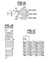
- Fig. 1A is a schematic view showing a known color television camera using the above explained spatial pixel shift.
- an image of an object is formed by an objective lens 1 and is divided by a three-color splitting optical system 2 into three primary color images, i.e. red, green and blue images. These color images are made incident upon solid state image sensors 3R, 3G and 3B, respectively.
- solid state image sensors 3R, 3G and 3B are spatially shifted in the horizontal direction with respect to pixels of the solid state image sensors 3R and 3B for receiving the red and blue images, respectively over a distance which is equal to a half of a pitch P of the pixels viewed in the horizontal direction.
- the spatial sampling is carried out such that successive pixels of the red and blue image sensors 3R and 3B are situated between successive pixels of the green image sensor 3G.
- the brightness signal is formed by adding the green, red and blue signals with each other, the number of pixels is apparently increased, and thus the resolution is improved, while the spurious component folded back into the lower frequency range can be reduced.
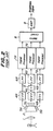
- Fig. 2 is a block diagram showing a known circuit for producing a brightness signals from the red, green and blue color signal generated by the red, green and blue image sensors 3R, 3G and 3B, respectively of the color television camera using the spatial pixel shift.
- the red, green and blue color signals are supplied to correlation double sampling circuits 4R, 4G and 4B, respectively, and then the green color signal is delayed by a delay circuit 5 having a delay time which is equal to a half of the sampling period, so that the phase of the green color signal is made coincident with the phase of the red and blue color signals.
- said sampling period corresponds the pitch of light receiving elements of the image sensors 3R, 3G and 3B viewed in the horizontal scanning direction.
- the red, green and blue color signals having the coincided phase are supplied to low pass filters 6R, 6G and 6B which cut off frequency components higher than the sampling frequency to remove sampling clock noise. Further, the red, green and blue color signals are supplied to image signal processing circuits 7R, 7G and 7B, respectively which perform the amplitude compression and y correction. Finally, the red, green and blue color signals are supplied to a matrix circuit 8 and are mixed with each other at a predetermined ratio to derive the brightness signal. In accordance with the standards of NTSC, the red, green and blue color signals are added with each other at a ratio of 0.3:0.59:0.11.
- the derived brightness signal is amplified by an amplifier 9 and then is supplied to an output terminal of the television camera. Since the spatial pixel shift is utilized, the spurious signal folded back toward the lower frequency range which might deteriorate the quality of the reproduced color image is reduced and the resolution of the brightness signal is apparently improved.
- the phase of the green color signal is delayed with respect to the red and blue color signals by passing the green color signal through the delay circuit 5 having the delay time corresponding to the 1/2P.
- the color signals are processed by the low pass filters 6R, 6G, 6B and image signal processing circuits 7R, 7G, 7B which also cause time delay for the color signals. Therefore, the phases of the red, green and blue color signals are not made identical with watch other precisely and the resolution of the brightness signal is decreased.
- the circuits provided between the color image sensors 3R, 3G, 3B and the matrix circuit 8 must have frequency characteristics which can process signals having frequencies sufficiently higher than the clock frequency of the solid state image sensors.
- the low pass filters 6R, 6G and 6B have the frequency characteristic in which higher frequency component is suppressed in order to remove the clock noise.
- the image signal processing circuits 7R, 7G and 7B could hardly derive the ideal color signals shown in Figs. 3C and 3D. Therefore, the higher frequency components of the actual green, red and blue color signals G', R' and B' obtained after being transmitted through the low pass filters 3G, 3R and 3B and image signal processing circuits 7G, 7R and 7B are suppressed as illustrated in Figs. 3F and 3G. This results in that the frequency response of the actual brightness signal Y' is reduced to a large extent as shown in Fig. 3H.
- the spatial pixel shift it is ideal to mix color signals at a ratio of 1:1.
- the green and red color signals are added with each other at a ratio of 2:1 and the green and blue color signals are mixed with each other at a ratio of 6:1. Therefore, the effect of the spatial pixel shift could not be achieved fully and the spurious signal could not be sufficiently removed and thus the resolution of the reproduced image is reduced.
- the present invention has for its object to proved a novel and useful circuit for deriving the brightness signal from the output signals of the color image sensors of the color television camera using the spatial pixel shift, in which the effect of the spatial pixel shift can be attained optimally and the resolution and frequency response of the brightness signal can be improved.
- a circuit for producing a brightness signal from an output signal of a solid state image pick-up apparatus in which at least two solid state image sensors each having a number of light receiving elements arranged in matrix are arranged in such a manner that light receiving elements of one solid state image sensor are shifted spatially in a main-scanning direction over a distance substantially equal to a half of a pitch of successive light receiving elements with respect to light receiving elements of the other solid state image sensor, comprises:
- delaying means for delaying an output signal generated by said one solid state image sensor by a delay time corresponding to a half of a spatial sampling period so that a phase of the output signal of said one solid state image sensor is made coincided with a phase of an output signal of said other solid state image sensor;
- first filtering means for for cutting off higher frequency components contained in an output signal of said filtering means and in the output signal of said other solid state image sensor
- signal processing means for processing output signals of said first filtering means
- first matrix means for adding output signals of said signal processing means with each other at a predetermined ratio to produce a first brightness signal
- second matrix means for adding the output signal of said delaying means and the output signal of said other solid state image sensor with each other at a ratio of 1:1 to derive a second brightness signal
- adding means for adding said high frequency component derived by said second filtering means with said first brightness signal.
- the second brightness signal is formed by mixing the output signals which are not processed by the first filtering means and signal processing means which might reduce the resolution and frequency response at the ratio of 1:1 at which the effect of the spatial pixel shift can be attained optimally. Then, the frequency component of the second brightness signal higher than a frequency range predetermined by a television standard system is extracted from the second brightness signal and the thus extracted higher frequency component is added to the first brightness signal. Therefore, when an object having a high spatial frequency is picked-up, it is possible to derive the brightness signal having the very high resolution and frequency response, while the effect of the spatial pixel shift can be achieved optimally.
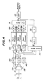
- Fig. 4 is a block diagram showing an embodiment of the circuit for producing the brightness signal from output signals generated by a color television camera using the spatial pixel shift.
- An image of an object is formed by an objective lens 11 and is divided into three primary color images by means of a color splitting optical system 12.
- the red, green and blue color images are then made incident upon red, green and blue solid state image sensors 13R, 13G and 13B, respectively to generate red, green and blue color signals.
- These color signals are then supplied to correlate double sampling circuits 14R, 14G and 14B, respectively and are sampled therein in accordance with a predetermined sampling clock.
- the green color signal is then delayed by a delay circuit 15 by a delay time which corresponds to a half of the pitch of the arrangement of light receiving elements viewed in the horizontal scanning direction. In this manner, the phase of the green color signal is made coincided with the phase of the red and blue color signals.
- the red, green and blue color signals are then supplied to low pass filters 16R, 16G and 16B, respectively to remove the sampling clock noise. Then output color signals from the low pass filters 16R, 16G and 16B are further processed by image signal processing circuits 17R, 17G and 17B, respectively to effect the various functions such as the y correction and amplitude compression. Output signals from the image signal processing circuits 17R, 17G and 17B are supplied to variable delay circuits 18R, 18G and 18B, respectively to correct differences in the phases of the color signals. Then, output signals of the variable delay circuits 18R, 18G and 18B are supplied to a first matrix circuit 19 and are mixed with each other at a ratio which has been determined by the television standard to derive a first brightness signal Y1. In NTSC system, the red, green and blue color signals are mixed with each other at a ratio of 0.3:0.59:0.11.
- the red and blue color signals derived from the correlate double sampling circuits 14R and 14B and the green color signal derived from the delay circuit 15 are supplied to a second matrix circuit 20 and are mixed with each other at a ratio of 1:1 to produce a second brightness signal Y 2 . That is to say, the red, green and blue color signals R, G and B are mixed at the following ratio:
- a ratio of a sum of the color signals generated by the image sensors in which the spatial pixel shift is taken place and a sum of color signals of the image sensors in which the spatial pixel shift is not effected becomes 1:1.
- the green color signal is equal to a sum of the red and blue color signals.
- the second brightness signal derived from the second matrix circuit 20 is then supplied to a band pass filter 21 for extracting a higher frequency component in the second brightness signal, said higher frequency component being higher than the predetermined maximum frequency of the first brightness signal which has been derived by mixing the color signals at the predetermined ratio.
- the higher frequency component thus extracted is then supplied to a delay circuit 23 giving a given delay time for correcting a possible difference in the delay time between the first brightness signal Y 1 and the second brightness signal Y 2 .
- the first brightness signal Y 1 generated from the first matrix circuit 19 and second brightness signal Y 2 derived from the delay circuit 22 are supplied to an adding amplifier 23 and are added with each other to derive a final brightness signal Y.
- the higher frequency component contained in the final brightness signal Y is obtained by mixing the color signals at the ratio which is different from the television standard.
- variable delay circuits 18R, 18G, 18B may be dispensed with.
- the delay time in the delay circuit 22 may be determined by considering the delay times in the low pass filters, image signal processing circuits, variable delay circuits, second matrix circuit and band pass filter.
- variable delay circuits 18R, 18G, 18B and delay circuit 22 it is possible to produce the brightness signal Y having the very high resolution and frequency response without being affected by the small difference in the phase, so that the effect of the spatial pixel shift can be attained optimally.
- the present invention is not limited to the embodiment just explained above, but many modifications and alternations may be conceived by those skilled in the art within the scope of the invention.
- the higher frequency component derived from the delay circuit 22 may be parallelly supplied to the image signal processing circuits 17R, 17G and 17B as shown by broken lines in Fig. 4.
- the color signals which have not been transmitted through the low pass filters and signal processing circuits are supplied to the second matrix circuit and the color signals generated from the image sensors in which the spatial pixel shift is performed are mixed with each other at the ratio of 1:1 to derive the second brightness signal, and then the higher frequency component is extracted from the second brightness signal and the thus extracted higher frequency component is added to the first brightness signal which has been derived by mixing the color signals at the ratio which is predetermined by the television standard. Therefore, the second brightness signal is not suffer from the difference in the delay time in the low pass filters and signal processing circuits, and thus the reduction of the resolution due to the difference in the delay time can be removed.
- the second brightness signal is not affected by the frequency band limitation and deterioration in the frequency characteristic, and therefore the deterioration in the resolution and frequency response can be avoided.
- the second brightness signal is formed by mixing the color signals at the ratio of 1:1 in regardless of the television standard, the effect of the spatial pixel shift can be always attained optimally.
Landscapes
- Engineering & Computer Science (AREA)
- Multimedia (AREA)
- Signal Processing (AREA)
- Color Television Image Signal Generators (AREA)
- Processing Of Color Television Signals (AREA)
Applications Claiming Priority (2)
| Application Number | Priority Date | Filing Date | Title |
|---|---|---|---|
| JP240093/90 | 1990-09-12 | ||
| JP2240093A JPH0724422B2 (ja) | 1990-09-12 | 1990-09-12 | カラーテレビカメラの輝度信号作成回路 |
Publications (1)
| Publication Number | Publication Date |
|---|---|
| EP0476421A1 true EP0476421A1 (fr) | 1992-03-25 |
Family
ID=17054388
Family Applications (1)
| Application Number | Title | Priority Date | Filing Date |
|---|---|---|---|
| EP91114845A Ceased EP0476421A1 (fr) | 1990-09-12 | 1991-09-03 | Circuit pour la production d'un signal de luminance issu d'un signal de sortie d'un dispositif de prise d'image à l'état solide avec decalage spatial des pixels |
Country Status (3)
| Country | Link |
|---|---|
| US (1) | US5184212A (fr) |
| EP (1) | EP0476421A1 (fr) |
| JP (1) | JPH0724422B2 (fr) |
Cited By (6)
| Publication number | Priority date | Publication date | Assignee | Title |
|---|---|---|---|---|
| EP0625859A1 (fr) * | 1993-05-19 | 1994-11-23 | Matsushita Electric Industrial Co., Ltd. | Caméra vidéo à état solide |
| WO1999013649A3 (fr) * | 1997-09-11 | 1999-06-03 | Koninkl Philips Electronics Nv | Decalage electronique d'un demi-pixel |
| EP1173029A3 (fr) * | 2000-07-14 | 2004-09-29 | Matsushita Electric Industrial Co., Ltd. | Appareil de prise de vues en couleurs |
| EP1528814A3 (fr) * | 2003-10-31 | 2007-01-03 | Hewlett-Packard Development Company, L.P. | Dispositif de formation d'images |
| CN102547157A (zh) * | 2011-12-31 | 2012-07-04 | 南京理工大学 | 自适应相关双采样相位校准方法 |
| CN102547302A (zh) * | 2010-09-30 | 2012-07-04 | 苹果公司 | 使用图像传感器接口定时信号的闪光同步 |
Families Citing this family (12)
| Publication number | Priority date | Publication date | Assignee | Title |
|---|---|---|---|---|
| EP0554035B1 (fr) * | 1992-01-27 | 2001-10-17 | Mitsubishi Denki Kabushiki Kaisha | Caméra vidéo couleur à l'état solide |
| US6788342B1 (en) | 1992-01-27 | 2004-09-07 | Mitsubishi Denki Kabushiki Kaisha | Color video camera for generating a luminance signal with unattenuated harmonics |
| JPH05219513A (ja) * | 1992-01-27 | 1993-08-27 | Ikegami Tsushinki Co Ltd | 固体撮像装置 |
| JP3666886B2 (ja) * | 1992-12-28 | 2005-06-29 | キヤノン株式会社 | 撮像装置 |
| JP3735867B2 (ja) * | 1993-01-14 | 2006-01-18 | ソニー株式会社 | 輝度信号生成装置 |
| JPH0851635A (ja) * | 1994-08-05 | 1996-02-20 | Sony Corp | 撮像装置 |
| JPH08140112A (ja) * | 1994-11-10 | 1996-05-31 | Sony Corp | ガンマ補正回路 |
| JPH10173859A (ja) * | 1996-12-09 | 1998-06-26 | Canon Inc | アナログ信号処理回路 |
| KR100223183B1 (ko) * | 1996-12-26 | 1999-10-15 | 윤종용 | 2판넬 액정프로젝터의 비데오신호처리장치 |
| JP4725217B2 (ja) * | 2005-07-11 | 2011-07-13 | 株式会社ニコン | 撮像装置 |
| FR2938065B1 (fr) * | 2008-11-05 | 2012-05-25 | I2S | Procede de numerisation de livres en trois dimensions par ondes terahertz. |
| JP2017099616A (ja) * | 2015-12-01 | 2017-06-08 | ソニー株式会社 | 手術用制御装置、手術用制御方法、およびプログラム、並びに手術システム |
Citations (2)
| Publication number | Priority date | Publication date | Assignee | Title |
|---|---|---|---|---|
| WO1985005526A1 (fr) * | 1984-05-19 | 1985-12-05 | Robert Bosch Gmbh | Procede pour augmenter la resolution de cameras de television couleur |
| WO1990013977A1 (fr) * | 1989-04-28 | 1990-11-15 | Ikegami Tsushinki Co., Ltd. | Dispositif de formation de signaux de luminance dans une camera video couleur |
Family Cites Families (6)
| Publication number | Priority date | Publication date | Assignee | Title |
|---|---|---|---|---|
| US4358788A (en) * | 1981-02-27 | 1982-11-09 | Rca Corporation | Legibility for alpha-mosaic characters |
| JPS581391A (ja) * | 1981-06-26 | 1983-01-06 | Sony Corp | 固体カラー撮像装置 |
| JPS5810988A (ja) * | 1981-07-14 | 1983-01-21 | Toshiba Corp | カラ−テレビジヨンカメラの信号処理回路 |
| JPS58137384A (ja) * | 1982-02-10 | 1983-08-15 | Sony Corp | カラ−カメラの信号処理回路 |
| JP2580560B2 (ja) * | 1985-05-28 | 1997-02-12 | ソニー株式会社 | 固体カラ−撮像装置 |
| JPS6229388A (ja) * | 1985-07-30 | 1987-02-07 | Matsushita Electric Ind Co Ltd | カラ−固体撮像装置 |
-
1990
- 1990-09-12 JP JP2240093A patent/JPH0724422B2/ja not_active Expired - Lifetime
-
1991
- 1991-09-03 EP EP91114845A patent/EP0476421A1/fr not_active Ceased
- 1991-09-06 US US07/756,334 patent/US5184212A/en not_active Expired - Lifetime
Patent Citations (2)
| Publication number | Priority date | Publication date | Assignee | Title |
|---|---|---|---|---|
| WO1985005526A1 (fr) * | 1984-05-19 | 1985-12-05 | Robert Bosch Gmbh | Procede pour augmenter la resolution de cameras de television couleur |
| WO1990013977A1 (fr) * | 1989-04-28 | 1990-11-15 | Ikegami Tsushinki Co., Ltd. | Dispositif de formation de signaux de luminance dans une camera video couleur |
Non-Patent Citations (3)
| Title |
|---|
| IEEE TRANSACTIONS ON CONSUMER ELECTRONICS, vol. 34, no. 3, August 1988, pages 506-511, IEEE, New York, US; Y. NISHIDA et al.: "Wide dynamic range HDTV image sensor with aliasing suppression" * |
| PATENT ABSTRACTS OF JAPAN, vol. 11, no. 127 (E-501)[2574], 21st April 1987; & JP-A-61 273 092 (SONY CORP.) 03-12-1986 * |
| PATENT ABSTRACTS OF JAPAN, vol. 7, no. 84 (E-169)[1229], 8th April 1983; & JP-A-58 10 988 (TOKYO SHIBAURA DENKI K.K.) 21-01-1983 * |
Cited By (12)
| Publication number | Priority date | Publication date | Assignee | Title |
|---|---|---|---|---|
| EP0625859A1 (fr) * | 1993-05-19 | 1994-11-23 | Matsushita Electric Industrial Co., Ltd. | Caméra vidéo à état solide |
| US5471323A (en) * | 1993-05-19 | 1995-11-28 | Matsushita Electric Industrial Co., Ltd | Solid state video camera having improved chromatic aberration suppression and moire suppression |
| WO1999013649A3 (fr) * | 1997-09-11 | 1999-06-03 | Koninkl Philips Electronics Nv | Decalage electronique d'un demi-pixel |
| US6542188B1 (en) | 1997-09-11 | 2003-04-01 | Koninklijke Philips Electronics N.V. | Color camera and method for obtaining an electronic half pixel offset |
| EP1173029A3 (fr) * | 2000-07-14 | 2004-09-29 | Matsushita Electric Industrial Co., Ltd. | Appareil de prise de vues en couleurs |
| US6917383B2 (en) | 2000-07-14 | 2005-07-12 | Matsushita Electric Industrial Co., Ltd. | Image sensing device |
| EP1528814A3 (fr) * | 2003-10-31 | 2007-01-03 | Hewlett-Packard Development Company, L.P. | Dispositif de formation d'images |
| US7961235B2 (en) | 2003-10-31 | 2011-06-14 | Hewlett-Packard Development Company, L.P. | Imaging apparatuses, image data processing methods, and articles of manufacture |
| CN102547302A (zh) * | 2010-09-30 | 2012-07-04 | 苹果公司 | 使用图像传感器接口定时信号的闪光同步 |
| CN102547302B (zh) * | 2010-09-30 | 2015-04-15 | 苹果公司 | 使用图像传感器接口定时信号的闪光同步 |
| CN102547157A (zh) * | 2011-12-31 | 2012-07-04 | 南京理工大学 | 自适应相关双采样相位校准方法 |
| CN102547157B (zh) * | 2011-12-31 | 2014-07-23 | 南京理工大学 | 自适应相关双采样相位校准方法 |
Also Published As
| Publication number | Publication date |
|---|---|
| JPH0724422B2 (ja) | 1995-03-15 |
| US5184212A (en) | 1993-02-02 |
| JPH04120995A (ja) | 1992-04-21 |
Similar Documents
| Publication | Publication Date | Title |
|---|---|---|
| EP0272634B1 (fr) | Dispositif de génération de signal vidéo | |
| US5184212A (en) | Circuit for producing brightness signal from output signal of solid state image pick-up apparatus using spatial pixel shift | |
| DE69426810T2 (de) | Bildaufnahmevorrichtung | |
| KR100481109B1 (ko) | 화상 신호 처리 장치 | |
| EP0729278A3 (fr) | Caméra vidéo couleur monochip générant des composantes de signaux couleurs inter-pixel par l'interpolation des signaux de couleurs primaires des pixels voisins | |
| US6147707A (en) | Method and apparatus for gain adjustment of an image sensor | |
| US4200883A (en) | Solid state color television camera | |
| JPH0458229B2 (fr) | ||
| EP0558338B1 (fr) | Caméra vidéo | |
| US5087967A (en) | Color image pickup device having a level correcting circuit for correcting level variations in color image signals | |
| US4527190A (en) | Mixing circuit | |
| US4884129A (en) | Signal processing apparatus for use with a single chip solid-state color camera | |
| EP0464879B1 (fr) | Système de séparation de signaux de luminance et de chrominance et méthode correspondante | |
| US5069530A (en) | Solid state image pick-up apparatus | |
| US5140410A (en) | Chrominance signal mixing circuit in a motion adaptive type signal separator | |
| US4646139A (en) | Color image pickup apparatus with color filter array comprising filter elements of three different colors arranged to provide reduced folding distortion | |
| US7688362B2 (en) | Single sensor processing to obtain high resolution color component signals | |
| KR920003720B1 (ko) | 디지탈 신호 처리 장치 | |
| EP0998135B1 (fr) | Circuit d'accentuation de contour | |
| US5534947A (en) | Advanced comb filter | |
| JP3263850B2 (ja) | 信号処理回路及び画像表示装置 | |
| JP2823264B2 (ja) | 映像信号処理回路 | |
| JP2723910B2 (ja) | 固体撮像装置 | |
| JPH06205422A (ja) | カラー撮像装置 | |
| JPH08242464A (ja) | カラーテレビジョン受信機 |
Legal Events
| Date | Code | Title | Description |
|---|---|---|---|
| PUAI | Public reference made under article 153(3) epc to a published international application that has entered the european phase |
Free format text: ORIGINAL CODE: 0009012 |
|
| AK | Designated contracting states |
Kind code of ref document: A1 Designated state(s): DE FR GB |
|
| 17P | Request for examination filed |
Effective date: 19920513 |
|
| 17Q | First examination report despatched |
Effective date: 19940427 |
|
| STAA | Information on the status of an ep patent application or granted ep patent |
Free format text: STATUS: THE APPLICATION HAS BEEN REFUSED |
|
| 18R | Application refused |
Effective date: 19960531 |