EP0476566A2 - Optische Übertragungssysteme und optischer Knoten zu diesem Zweck - Google Patents
Optische Übertragungssysteme und optischer Knoten zu diesem Zweck Download PDFInfo
- Publication number
- EP0476566A2 EP0476566A2 EP91115682A EP91115682A EP0476566A2 EP 0476566 A2 EP0476566 A2 EP 0476566A2 EP 91115682 A EP91115682 A EP 91115682A EP 91115682 A EP91115682 A EP 91115682A EP 0476566 A2 EP0476566 A2 EP 0476566A2
- Authority
- EP
- European Patent Office
- Prior art keywords
- optical
- signal
- intensity
- transmission path
- node
- Prior art date
- Legal status (The legal status is an assumption and is not a legal conclusion. Google has not performed a legal analysis and makes no representation as to the accuracy of the status listed.)
- Granted
Links
Images



Classifications
-
- H—ELECTRICITY
- H04—ELECTRIC COMMUNICATION TECHNIQUE
- H04B—TRANSMISSION
- H04B10/00—Transmission systems employing electromagnetic waves other than radio-waves, e.g. infrared, visible or ultraviolet light, or employing corpuscular radiation, e.g. quantum communication
- H04B10/27—Arrangements for networking
-
- H—ELECTRICITY
- H04—ELECTRIC COMMUNICATION TECHNIQUE
- H04B—TRANSMISSION
- H04B10/00—Transmission systems employing electromagnetic waves other than radio-waves, e.g. infrared, visible or ultraviolet light, or employing corpuscular radiation, e.g. quantum communication
- H04B10/27—Arrangements for networking
- H04B10/278—Bus-type networks
-
- H—ELECTRICITY
- H04—ELECTRIC COMMUNICATION TECHNIQUE
- H04B—TRANSMISSION
- H04B10/00—Transmission systems employing electromagnetic waves other than radio-waves, e.g. infrared, visible or ultraviolet light, or employing corpuscular radiation, e.g. quantum communication
- H04B10/29—Repeaters
- H04B10/291—Repeaters in which processing or amplification is carried out without conversion of the main signal from optical form
- H04B10/297—Bidirectional amplification
- H04B10/2971—A single amplifier for both directions
-
- H—ELECTRICITY
- H04—ELECTRIC COMMUNICATION TECHNIQUE
- H04B—TRANSMISSION
- H04B10/00—Transmission systems employing electromagnetic waves other than radio-waves, e.g. infrared, visible or ultraviolet light, or employing corpuscular radiation, e.g. quantum communication
- H04B10/29—Repeaters
- H04B10/291—Repeaters in which processing or amplification is carried out without conversion of the main signal from optical form
- H04B10/297—Bidirectional amplification
- H04B10/2972—Each direction being amplified separately
Definitions
- the present invention relates to an optical communication system or network and art optical node for use therein, and, more particularly, to an optical communication system, typically, of a bus type, in which the amplification gain of an optical amplifier in each terminal is controlled in a predetermined manner and an optical node to be used therein.
- an optical signal transmitted through an optical fiber is transmitted through each terminal connected to the optical fiber without being converted to an electric signal, and in each terminal, a means for effecting optical branching and optical combining which is called an optical node is connected to the optical fiber and performs reception and transmission of signals from and to the optical fiber.
- the intensity of the optical signal transmitted through the optical fiber is reduced. So, previously the number of terminals that could be connected to the optical fiber was limited, and hence the bus type of optical communication network was believed impractical. However, recently, a means for amplifying the optical signal without converting this to an electric signal, such as a semiconductor optical amplifier and a fiber optical amplifier, has been developed, so it has become possible to increase the number of terminals to be connected to the optical fiber.
- the bus type system has an advantage that the terminal connection to the optical fiber can easily be modified. So, the bus type system is suitable for a local area network in which the total transmission distance length is about several kilometers and in which flexibility to re-connect the terminals is desired.
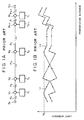
- Figs. 1A and 1B respectively show a schematic structure of such a prior art bus type of an optical communication network and intensities of optical signals on its optical fiber transmission path.
- optical fibers F1 - F i+1 terminals T1 - T i , optical nodes N1 - N i and end equipment S1 and S2 for preventing reflections of an optical signal at optical fiber ends.
- the optical nodes respectively have functions that the electric signals from the terminals T1 - T i are converted into optical signals to be transmitted to the optical fibers F1 - F i+1 , that parts of the optical signals on the optical fibers F1 - F i+1 are picked out to be converted into electric signals for transmission to the terminals T1 - T i , and that the optical signals on the optical fibers F1 - F i+1 are amplified to be transmitted to adjacent optical fibers.
- Fig. 1A there are provided optical fibers F1 - F i+1 , terminals T1 - T i , optical nodes N1 - N i and end equipment S1 and S2 for preventing reflections of an optical signal at optical fiber ends.
- the optical nodes respectively have functions that the electric signals
- a line L1 indicates that an optical signal output from the optical node N1 is attenuated on the optical fibers F - F i+1 and that such optical signal is amplified by other optical nodes (i.e., the intensity of the optical signal output from the node N1), and a line L2 indicates the intensity of an optical signal output from the optical node N3.
- the signal from the terminal T1 is converted into the optical signal by the optical node N1 and output to the optical fibers F1 and F2.
- the optical signal transmitted to the optical fiber F1 is absorbed by the end equipment S1.
- the optical signal transmitted to the optical fiber F2 is reduced by an attenuation amount determined by the length of the optical fiber F2 and enters the optical node N2.
- the optical node N2 picks out part of the incident signal to convert this into an electric signal and transmits this part to the terminal T2.
- the node N2 amplifies the remaining part of the incident signal at a predetermined gain and transmits this to the optical fiber F3.
- This optical signal is transmitted by being repeatedly processed in this manner and reaches the end equipment S2 after passing through the other optical nodes.
- the signal from the terminal T3 is converted into an electric signal in the optical node N3 and is transmitted to two adjacent optical fibers F3 and F4 to finally reach respective end equipment S1 and S2 by the same process as described above.
- Such methods includes a method wherein the signal transmission from a certain terminal is started after the confirmation that no signals are transmitted from the other terminals (called carrier sense multiple access (CSMA)), a method wherein the signal transmission is conducted during a time slot allotted to each individual terminal (called time division multiplexing access (TDWA)), and a method wherein a signal is transmitted from each individual terminal using light whose wavelength is different from those of the other terminals (called wavelength division multiplexing (WDM)).
- CSMA carrier sense multiple access
- TDWA time division multiplexing access
- WDM wavelength division multiplexing
- the gain value of each node is beforehand determined, as mentioned above. So, if those predetermined gain values are set equal to one another, it would be impossible to freely select the distance between the nodes. In other words, where the distance between the nodes is shortened to obtain a multistage connection, the intensity of a transmitted optical signal may amount to the saturation level of an optical amplifier used in the optical node. As a result, the signal distortion increases and hence the error rate at the time of transmission may be enhanced.
- the gain of each individual optical node is independently determined so as to prevent the above-discussed saturation, the saturation and shortage of the optical signal may occur in turn if the connection configuration of the optical communication network is altered and hence the distance between the nodes is changed.
- the reason therefor is that the gain is set to a small value in such an optical node having a short distance to an adjacent optical node while set to a large value in an optical node having a long distance to an adjacent node.
- An object of the present invention is to provide an optical communication network which is structured so as not to cause any inconveniences even if optical nodes are flexibly re-connected.
- Another object of the present invention is to provide an optical node which is suitable for use in the optical communication network mentioned above.
- a further object of the present invention is to provide an optical repeating method for equalizing an output from an optical node with an input to the optical node.
- an optical communication network comprises at least one optical transmission path, a plurality of terminals connected to the optical transmission path, optical nodes for receiving and transmitting an optical signal between the optical transmission path and the terminals, and means for controlling an intensity of a signal output from each optical node so as to equalize its intensity with that of a signal input to each optical node from the optical transmission path.
- an optical node to be used in an optical commun ication network comprises means for receiving and transmitting an optical signal between an optical transmission path and a plurality of terminals connected thereto, and means for controlling an intensity of a signal output from the receiving and transmitting means so as to equalize its intensity with the intensity of a signal input to the receiving and transmitting means from the optical transmission path.
- an optical repeating method comprises the steps of first monitoring the intensity of a signal input to an optical node, secondly monitoring the intensity of a signal output from the optical node, amplifying the input signal, and controlling a gain of the amplifying step based on the intensity of the input and output signals obtained in the first and second monitoring steps.
- Fig. 1A is a view showing a structure of a prior art bus-type optical communication network.
- Fig. 1B is a representation illustrating the intensity of an optical signal on an optical transmission path in Fig. 1A.
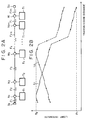
- Fig. 2A is a view showing a structure of a first embodiment according to the present invention.
- Fig. 2B is a representation illustrating the intensity of an optical signal on an optical transmission path in Fig. 2A.
- Fig. 3 is a view showing a structure of an optical node used in the first embodiment of Fig. 2A.
- Fig. 4 is a view showing a structure of an optical node in a second embodiment according to the present invention.
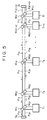
- Fig. 5 is a view showing a structure of a third embodiment according to the present invention.
- Fig. 6 is a view showing a structure of an optical node in the third embodiment of Fig. 5.
- Fig. 2A shows the first embodiment of this invention
- Fig. 2B illustrates the intensity of an optical communication signal at each point in the network shown in Fig. 2A.
- terminals T1, ⁇ ⁇ ⁇ , T i there are provided terminals T1, ⁇ ⁇ ⁇ , T i , optical fiber transmission paths F1, ⁇ ⁇ ⁇ , F i+1 , and optical nodes N1, ⁇ ⁇ ⁇ , N i .
- the functions of each optical node are basically the same as those explained above referring to Fig. 1A.
- End equipment S1 and S2 are also the same as those explained above.
- a line L1 indicates the intensity of an optical signal transmitted from the terminal T1 shown in Fig. 2A through the optical node N1, and a line L2 indicates the intensity of the same from another terminal T3.
- Fig. 3 shows the construction of each optical node N1 - N i in the bus-type optical communication network shown in Fig. 2A.
- E/O electro-optical
- O/E opto-electrical
- ,Y6 for branching an optical signal to two optical signals or combining two optical signals to a single one
- directional couplers C1 and C2 for picking out part (e.g., 1/10) of each of optical signals propagating in opposite directions
- optical amplifiers A1 and A2 for amplifying an optical signal as it is without converting it to an electric signal
- optical isolators for transmitting an optical signal solely in one direction
- comparators G1 and G2 for discriminating the magnitudes of two input electric signals to control gains of the optical amplifiers A1 and A2 accordingly
- optical fiber transmission paths F L and F R optical fiber transmission paths
- E/O converter E1 a semiconductor laser (LD), a light emitting device (LED) or the like can be used.
- O/E converter a PIN photodiode (PIN-PD), an avalanche photodiode (APD) or the like can be employed.
- optical amplifier A1, A2 a semiconductor optical amplifier, a fiber optical amplifier or the like can preferably be applied thereto.
- coupler Y1 - Y6 a fiber-fusion type of optical coupler or the like can be used, and as the directional coupler C1, C2, a waveguide type of optical coupler can be utilized.
- the optical node N when the terminal T is not in a transmission state, the optical node N operates as follows.
- this optical signal When the optical signal from another terminal is transmitted to the optical fiber transmission path F L , this optical signal reaches the coupler Y3 through the directional coupler C1. At this time, part (e.g., 1/10) of the signal is picked out by the directional coupler C1 and then converted into an electric signal by the O/E converter D3 to be input into one of the input terminals of the comparator G1.
- the optical signal reaching the coupler Y3 transmits through the isolator I2 and is branched by the coupler Y5 into two signals. One of the signals is input into the optical amplifier A2, while the other signal is input into the O/E converter D1 through the couplers Y2 and Y1 to be converted into an electric signal and then transmitted to the terminal T.
- the optical signal reaching the optical amplifier A2 is amplified thereby, and is transmitted to the optical fiber transmission path F R through the coupler Y4 and the directional coupler C2. At this time, part of the optical signal is picked out by the directional coupler C2 and converted into an electric signal by the O/E converter D2 to be input into one of two terminals of the comparator G1.
- the comparator G1 compares intensities of the electric signals from the O/E converters D2 and D3, and when the intensity from the converter D2 is larger than that from the converter D3, the comparator G1 decreases the gain of the optical amplifier A2.
- the comparator G1 increases such gain when the reverse holds true.
- the gain of the optical amplifier A2 where such as a semiconductor optical amplifier is used, can electrically be controlled by changing its injection current. In such manner, the gain of the optical amplifier A2 in the optical node N is controlled such that the intensity of the optical signal incident from the optical fiber transmission path F L is always made equal to that transmitted to the optical fiber transmission path F R .
- the signal is incident from the optical fiber transmission path F R , the signal transmits through the directional coupler C2, the coupler Y4, the isolator I1, and the coupler Y6, and then is amplified by the optical amplifier A1 to be sent out to the optical fiber transmission path F L through the coupler Y3 and the directional coupler C1.
- the gain of the optical amplifier A1 is controlled such that input and output intensities are made equal to each other by the comparator G2 by comparing the intensities of signals which are respectively picked out by the directional couplers C2 and C1 and converted into electric signals by the O/E converters D4 and D5.
- the gains of the optical amplifiers A1 and A2 are so determined that their outputs amount to respective predetermined values.
- the amplifiers A1 and A2 are not controlled by the comparators G1 and G2. This operation is done, e.g., by controlling the optical amplifiers A1 and A2 in response to signals from a controller or the like provided in the terminal T.
- the signal from the terminal T is converted into an optical signal by the E/O converter E1, transmits through the coupler Y1, Y2, Y5 and Y6, and is amplified by the optical amplifiers A1 and A2 to a predetermined output level. Then, the amplified signals are respectively transmitted to the optical fiber transmission paths F L and F R through the couplers Y3 and Y4 and the directional couplers C1 and C2.
- the couplers Y5 and Y6, in general, branch the optical signal from the coupler Y2 also in directions opposite to directions bound for the amplifiers A1 and A2, so that the isolators I1 and I2 are used so as not to send those branched unwanted signals out to the optical fiber transmission paths.
- the terminal T1 transmits a signal.
- the signal from the terminal T1 is converted into an optical signal by the optical node N1 and transmitted to the optical fiber transmission paths F1 and F2.
- the gains of the optical amplifiers A1 and A2 contained in the optical node N1 are controlled such that a predetermined optical output P0 can be obtained as explained above. This output is indicated by P0 in Fig. 2B.
- the optical signal transmitted to the transmission path F1 is absorbed at the end equipment S1.
- the optical signal transmitted to the optical fiber transmission path F2 is attenuated by such an attenuation amount as is determined by the length of the optical fiber F2, and reaches the optical node N2.
- part of the optical signal is branched to be transmitted to the terminal T2, and the remaining is, as explained above, amplified to an intensity equal to the intensity of the light input to the optical node N2 and is transmitted to the optical fiber transmission path F3.
- this signal is absorbed by the end equipment S2, after passing through all the other optical nodes N3 - N i with the same process being repeated.
- the intensity of the optical signal at this end is indicated by P1 in Fig. 2B.
- the difference between P0 and P1 namely, a total loss amount of the optical signal output from the optical node N1 is determined by a total extension distance of the optical fiber transmission paths F2 - F i+1 .
- the intensity of the optical signal transmitted from the optical node N3 is P0, and the loss amount of the optical signal is determined by the length of the optical fiber as mentioned above (the total length of the optical fibers F3, F2 and F1 in a case where the signal is transmitted in the leftward direction, while the total length of the optical fibers F4 - F i+1 in a case where the signal is transmitted in the rightward direction). So, intensities of these signals would never be less than P1.
- the loss in the optical fiber would not become a problem in the optical communication network according to this invention because the total distance could not be made too long due to the signal transmission delay in the bus-type optical communication network as mentioned above.
- Fig. 4 shows the structure of an optical node of a second embodiment.
- the same optical communication network as shown in Fig. 2A is utilized.
- Fig. 4 there are provided bidirectional optical amplifiers A3 and A4 in which there is no distinction between output and input terminals.
- Semiconductor optical amplifiers or the like can preferably be employed for effecting the amplification of optical communication signals in opposite directions.
- couplers C3 and C4 for picking out part (e.g., 1/10) of a transmitted signal.
- the same reference numerals as those in Fig. 3 designate the same members or means as those in Fig. 4.
- the signal light from the other optical nodes incident from the optical fiber transmission paths F R and F L is branched by the coupler, and the signal lights travelling in opposite directions are separately amplified.
- the signal lights propagating in opposite directions are amplified by a common optical amplifier without branching or combining them.
- the couplers Y2, Y3 and Y4 in the first embodiment are not used in the second embodiment.
- the gain of each bidirectional optical amplifier A3, A4 can be made approximately equal with respect to both directions, so that the optical node having the same function as that shown in Fig. 3 can be achieved by such a structure as shown in Fig. 4.
- the remaining operation is substantially the same as that of the first embodiment.
- FIG. 5 showing the optical communication network of the third embodiment, there are provided terminals T1, ⁇ ⁇ ⁇ , T i , optical fiber transmission paths F11, F21, ⁇ ⁇ ⁇ , F 1(i+1) , F 2(i+1) , optical nodes M11, M21, ⁇ ⁇ ⁇ , M 1i , M 2i , and end equipment S3 and S4.
- Each optical node converts a signal from the terminal into an optical signal and transmits this optical signal to the optical fiber transmission path, converts a signal on the optical fiber transmission path into an electric signal and transmits this electric signal to the terminal, and acts as a repeater by amplifying the signal on the optical fiber transmission path.
- Fig. 6 shows the structure of each optical node M11, ⁇ ⁇ ⁇ , M 2i shown in Fig. 5.
- the same reference numerals as those in Fig. 3 indicate the same members or means as those in Fig. 3. It is noted, however, that directional couplers C6 and C7 operate solely in one direction.
- the optical node as shown in Fig. 6 is used without any modifications as the optical nodes designated by M21, ⁇ ⁇ ⁇ , M 2i in Fig. 5, and that the optical node turned around with respect to right and left sides from that of Fig. 6 is used as the optical nodes designated by M11, ⁇ ⁇ ⁇ , M 1i in Fig. 5.
- the present invention is applied to such an optical communication network in which signals on the optical fiber are transmitted in opposite directions
- such a bus-type network is attained where in there are used a pair of optical fiber transmission paths each of which transmits a signal in a single direction.
- the optical node having the same function as that in the first and second embodiments can be used for composing an optical communication network which obtains the same operation and advantages as mentioned above.
- each terminal contains a single light emitting device or E/O converter
- the present invention can apply also to an optical communication network in which each terminal includes a plurality of light emitting devices for emitting lights of different wavelengths or a tunable light emitting device whose wavelength is changeable for performing a wavelength division multiplexing communication.
- each optical node contains plural optical amplifiers, plural comparators, and so forth for respective signal lights of different wavelengths, and a wavelength multiplexer and a de-multiplexer need be disposed at an output port and an input port of the optical node, respectively.
- the light emitting device, the light receiving device (O/E converter), the optical converter, etc. are respectively semiconductor devices such as a semiconductor laser, a PIN photodiode, a semiconductor optical amplifier, etc., in the above-discussed embodiments, but they are not limited to semiconductor devices. Different kinds of devices can also be applied so far as they have the same functions, respectively.
- optical fibers are used as an optical transmission path
- the present invention is also applicable to optical communication networks other than the optical fiber communication system.
- any type of optical node can be utilized in an optical communication network for system of the present invention so long as the optical node functions in the same manner as discussed above
- the end equipment S1, S2, S3, S4 may be replaced by other means such as a gateway for connecting this optical communication system to another network.
- a means for amplifying an optical signal in such a manner that the intensity of light input to an optical node which contains this amplifying means becomes equal to that of light output from this optical node. So, even if the configuration of connection of optical nodes is changed in the network, the power of an optical signal would not saturate nor run short at any optical nodes.
- an optical communication network or system typically a bus-type one, is achieved in which optical nodes can be flexibly re-connected without any disadvantages.
- An optical communication network includes at least one optical transmission path, a plurality of terminals connected to the optical transmission path, a plurality of optical nodes for receiving and transmitting an optical signal between the optical transmission path and the terminals, and a controller for controlling the intensity of a signal output from each optical node so as to equalize its intensity with the intensity of a signal input to each optical node from the optical transmission path.
- the loss of a signal's intensity is determined solely by the total extension length of the optical transmission path, so that the optical nodes can be freely re-connected in the network.
Landscapes
- Engineering & Computer Science (AREA)
- Physics & Mathematics (AREA)
- Electromagnetism (AREA)
- Computer Networks & Wireless Communication (AREA)
- Signal Processing (AREA)
- Computing Systems (AREA)
- Optical Communication System (AREA)
- Small-Scale Networks (AREA)
Applications Claiming Priority (3)
| Application Number | Priority Date | Filing Date | Title |
|---|---|---|---|
| JP2246657A JPH04124935A (ja) | 1990-09-17 | 1990-09-17 | 光通信ネットワーク及びそこで用いられる光ノード |
| JP246657/90 | 1990-09-17 | ||
| JP24665790 | 1990-09-17 |
Publications (3)
| Publication Number | Publication Date |
|---|---|
| EP0476566A2 true EP0476566A2 (de) | 1992-03-25 |
| EP0476566A3 EP0476566A3 (en) | 1993-08-04 |
| EP0476566B1 EP0476566B1 (de) | 1999-12-01 |
Family
ID=17151679
Family Applications (1)
| Application Number | Title | Priority Date | Filing Date |
|---|---|---|---|
| EP91115682A Expired - Lifetime EP0476566B1 (de) | 1990-09-17 | 1991-09-16 | Optische Übertragungssysteme und darin verwendbare optische Knoten |
Country Status (5)
| Country | Link |
|---|---|
| US (1) | US5502589A (de) |
| EP (1) | EP0476566B1 (de) |
| JP (1) | JPH04124935A (de) |
| AT (1) | ATE187291T1 (de) |
| DE (1) | DE69131812T2 (de) |
Cited By (1)
| Publication number | Priority date | Publication date | Assignee | Title |
|---|---|---|---|---|
| CN115118656A (zh) * | 2021-03-23 | 2022-09-27 | 嘉雨思科技股份有限公司 | 路由集成电路元件 |
Families Citing this family (21)
| Publication number | Priority date | Publication date | Assignee | Title |
|---|---|---|---|---|
| US6369938B1 (en) * | 1996-05-28 | 2002-04-09 | Fujitsu Limited | Multi-wavelength light amplifier |
| JP3022359B2 (ja) * | 1996-11-29 | 2000-03-21 | 日本電気株式会社 | 光分波合波装置 |
| US5898801A (en) | 1998-01-29 | 1999-04-27 | Lockheed Martin Corporation | Optical transport system |
| US6631018B1 (en) | 1997-08-27 | 2003-10-07 | Nortel Networks Limited | WDM optical network with passive pass-through at each node |
| EP0914015B1 (de) * | 1997-10-28 | 2006-12-20 | Nec Corporation | Optischer Ein-/Ausfügemultiplexer |
| US6603596B2 (en) * | 1998-03-19 | 2003-08-05 | Fujitsu Limited | Gain and signal level adjustments of cascaded optical amplifiers |
| US7072588B2 (en) | 2000-10-03 | 2006-07-04 | Halliburton Energy Services, Inc. | Multiplexed distribution of optical power |
| US20020101874A1 (en) * | 2000-11-21 | 2002-08-01 | Whittaker G. Allan | Physical layer transparent transport information encapsulation methods and systems |
| EP1415420A1 (de) * | 2001-08-08 | 2004-05-06 | Lockheed Martin Corporation | System und verfahren zur kommunikation über einen bidirektionalen optischen bus |
| US7085497B2 (en) * | 2002-04-03 | 2006-08-01 | Lockheed Martin Corporation | Vehicular communication system |
| US20040076434A1 (en) * | 2002-09-27 | 2004-04-22 | Whittaker G. Allan | Optical distribution network for RF and other analog signals |
| US6912339B2 (en) * | 2002-09-27 | 2005-06-28 | Lockheed Martin Corporation | Optical interface devices having balanced amplification |
| US7283480B1 (en) | 2002-11-12 | 2007-10-16 | Lockheed Martin Corporation | Network system health monitoring using cantor set signals |
| US7349629B1 (en) | 2002-11-26 | 2008-03-25 | Lockheed Martin Corporation | Methods and systems for creating a digital interconnect fabric |
| JP2004297714A (ja) * | 2003-03-28 | 2004-10-21 | Fujitsu Ltd | 多方向光分岐装置 |
| WO2004093351A2 (en) * | 2003-03-31 | 2004-10-28 | Lockheed Martin Corporation | Optical network interface systems and devices |
| US7424228B1 (en) | 2003-03-31 | 2008-09-09 | Lockheed Martin Corporation | High dynamic range radio frequency to optical link |
| DE10360873B4 (de) * | 2003-12-23 | 2006-08-10 | Airbus Deutschland Gmbh | Verfahren zum Betreiben eines Terminals, Terminal und Datenbussystem |
| US7440699B1 (en) | 2004-06-28 | 2008-10-21 | Lockheed Martin Corporation | Systems, devices and methods for transmitting and receiving signals on an optical network |
| CN102237932B (zh) * | 2010-04-30 | 2016-07-06 | 中兴通讯股份有限公司 | 长距光放大装置、无源光网络和光信号传输方法 |
| TWI566537B (zh) * | 2012-05-25 | 2017-01-11 | 鴻海精密工業股份有限公司 | 光纖傳輸系統 |
Family Cites Families (11)
| Publication number | Priority date | Publication date | Assignee | Title |
|---|---|---|---|---|
| DE2248372C2 (de) * | 1972-10-03 | 1984-09-20 | Siemens AG, 1000 Berlin und 8000 München | Zwischenverstärker für ein optisches Nachrichtenübertragungssystem |
| FR2239063B1 (de) * | 1973-07-27 | 1977-09-16 | Thomson Csf | |
| DE3007958C2 (de) * | 1980-03-01 | 1985-01-17 | Hartmann & Braun Ag, 6000 Frankfurt | Opto-elektonisches Übertragungssystem |
| EP0192795B1 (de) * | 1985-02-28 | 1989-08-02 | International Business Machines Corporation | Nachrichtensystem mit überlappenden Vielfachzugriffübertragungsnetzwerken |
| JPS62216511A (ja) * | 1986-03-18 | 1987-09-24 | Nec Corp | 自動利得制御装置 |
| US4947134A (en) * | 1987-10-30 | 1990-08-07 | American Telephone And Telegraph Company | Lightwave systems using optical amplifiers |
| JPH07109916B2 (ja) * | 1988-05-26 | 1995-11-22 | 浜松ホトニクス株式会社 | 光強度安定化装置 |
| GB2230912B (en) * | 1989-04-22 | 1993-10-20 | Stc Plc | Optical amplifier gain control |
| GB2240228B (en) * | 1990-01-23 | 1993-11-03 | Stc Plc | Optical transmission system. |
| GB2251148B (en) * | 1990-09-18 | 1995-04-12 | Fujitsu Ltd | Optical repeater having loop-back function |
| US5268786A (en) * | 1991-03-15 | 1993-12-07 | Mitsubishi Denki Kabushiki Kaisha | Optical fiber amplifier and its amplification method |
-
1990
- 1990-09-17 JP JP2246657A patent/JPH04124935A/ja active Pending
-
1991
- 1991-09-16 DE DE69131812T patent/DE69131812T2/de not_active Expired - Fee Related
- 1991-09-16 EP EP91115682A patent/EP0476566B1/de not_active Expired - Lifetime
- 1991-09-16 AT AT91115682T patent/ATE187291T1/de active
-
1995
- 1995-06-05 US US08/465,575 patent/US5502589A/en not_active Expired - Fee Related
Cited By (1)
| Publication number | Priority date | Publication date | Assignee | Title |
|---|---|---|---|---|
| CN115118656A (zh) * | 2021-03-23 | 2022-09-27 | 嘉雨思科技股份有限公司 | 路由集成电路元件 |
Also Published As
| Publication number | Publication date |
|---|---|
| EP0476566B1 (de) | 1999-12-01 |
| ATE187291T1 (de) | 1999-12-15 |
| JPH04124935A (ja) | 1992-04-24 |
| DE69131812D1 (de) | 2000-01-05 |
| US5502589A (en) | 1996-03-26 |
| DE69131812T2 (de) | 2000-06-15 |
| EP0476566A3 (en) | 1993-08-04 |
Similar Documents
| Publication | Publication Date | Title |
|---|---|---|
| US5502589A (en) | Optical communication systems and optical nodes for use therein | |
| EP0234804B1 (de) | Wellenleiterübertragungssystem | |
| US6233076B1 (en) | Optical communications system | |
| US5610744A (en) | Optical communications and interconnection networks having opto-electronic switches and direct optical routers | |
| EP0842575B1 (de) | Verbesserungen an optischen einlieferungs- und abtrennwellenlängenmultiplexsystemen | |
| EP1171967B1 (de) | Verfahren und vorrichtung zur qualitätsüberwachung von datenübertragung über analoge leitungen | |
| FI102650B (fi) | Telejohto optisin kuiduin ja erillisin huoltokanavin | |
| EP0392490B1 (de) | Optische Verzweigungsvorrichtung und deren Verwendung in einem optischen Netzwerk | |
| EP0503849A2 (de) | Photonischer Verzweigerschalter | |
| EP0847158A2 (de) | Vorrichtung zum optischen Wellenlängen-Multiplexen und Demultiplexen und optisches Nachrichtenübertragungssystem, das diese verwendet | |
| EP1246377B1 (de) | Optisches Verstärkungs und Übertragungssystem | |
| EP2727271B1 (de) | Optisches kommunikationssystem, vorrichtung und verfahren zur datenverarbeitung in einem optischen netzwerk | |
| JP2733263B2 (ja) | 集積型光ノードおよびそれを用いたバス型光情報システム | |
| EP0351133A2 (de) | Optisches polarisationsunempfindliches Übertragungsgerät mit optischer Vorverstärkung | |
| US6577416B1 (en) | Channel control in a wavelength division multiplexed communications network | |
| NZ235720A (en) | Optical signal repeater uses optical/electrical/optical link | |
| US12284467B2 (en) | Optical network configuration | |
| JPH09179151A (ja) | 方向切替型光増幅器と同増幅器を用いたバス型一芯光通信システム | |
| KR19980075310A (ko) | 단일 활성섬유를 이용한 양방향성 광섬유증폭기 | |
| JPS628979B2 (de) | ||
| RU2219667C2 (ru) | Способ контроля сети волоконно-оптической системы передачи | |
| JPH05344076A (ja) | スターリング通信装置 | |
| JP3077620B2 (ja) | 波長多重伝送用光ブースタアンプ | |
| JPH04246931A (ja) | 光通信システム | |
| Garnham et al. | 100dB optical path loss transmission system experiment employing two linear optoelectronic repeaters |
Legal Events
| Date | Code | Title | Description |
|---|---|---|---|
| PUAI | Public reference made under article 153(3) epc to a published international application that has entered the european phase |
Free format text: ORIGINAL CODE: 0009012 |
|
| AK | Designated contracting states |
Kind code of ref document: A2 Designated state(s): AT BE CH DE DK ES FR GB GR IT LI LU NL SE |
|
| PUAL | Search report despatched |
Free format text: ORIGINAL CODE: 0009013 |
|
| AK | Designated contracting states |
Kind code of ref document: A3 Designated state(s): AT BE CH DE DK ES FR GB GR IT LI LU NL SE |
|
| 17P | Request for examination filed |
Effective date: 19931221 |
|
| 17Q | First examination report despatched |
Effective date: 19961025 |
|
| GRAG | Despatch of communication of intention to grant |
Free format text: ORIGINAL CODE: EPIDOS AGRA |
|
| GRAG | Despatch of communication of intention to grant |
Free format text: ORIGINAL CODE: EPIDOS AGRA |
|
| GRAG | Despatch of communication of intention to grant |
Free format text: ORIGINAL CODE: EPIDOS AGRA |
|
| GRAH | Despatch of communication of intention to grant a patent |
Free format text: ORIGINAL CODE: EPIDOS IGRA |
|
| GRAH | Despatch of communication of intention to grant a patent |
Free format text: ORIGINAL CODE: EPIDOS IGRA |
|
| GRAH | Despatch of communication of intention to grant a patent |
Free format text: ORIGINAL CODE: EPIDOS IGRA |
|
| GRAA | (expected) grant |
Free format text: ORIGINAL CODE: 0009210 |
|
| AK | Designated contracting states |
Kind code of ref document: B1 Designated state(s): AT BE CH DE DK ES FR GB GR IT LI LU NL SE |
|
| PG25 | Lapsed in a contracting state [announced via postgrant information from national office to epo] |
Ref country code: AT Free format text: LAPSE BECAUSE OF FAILURE TO SUBMIT A TRANSLATION OF THE DESCRIPTION OR TO PAY THE FEE WITHIN THE PRESCRIBED TIME-LIMIT Effective date: 19991201 Ref country code: NL Free format text: LAPSE BECAUSE OF FAILURE TO SUBMIT A TRANSLATION OF THE DESCRIPTION OR TO PAY THE FEE WITHIN THE PRESCRIBED TIME-LIMIT Effective date: 19991201 Ref country code: GR Free format text: LAPSE BECAUSE OF NON-PAYMENT OF DUE FEES Effective date: 19991201 Ref country code: BE Free format text: LAPSE BECAUSE OF FAILURE TO SUBMIT A TRANSLATION OF THE DESCRIPTION OR TO PAY THE FEE WITHIN THE PRESCRIBED TIME-LIMIT Effective date: 19991201 Ref country code: ES Free format text: THE PATENT HAS BEEN ANNULLED BY A DECISION OF A NATIONAL AUTHORITY Effective date: 19991201 Ref country code: CH Free format text: LAPSE BECAUSE OF FAILURE TO SUBMIT A TRANSLATION OF THE DESCRIPTION OR TO PAY THE FEE WITHIN THE PRESCRIBED TIME-LIMIT Effective date: 19991201 Ref country code: SE Free format text: THE PATENT HAS BEEN ANNULLED BY A DECISION OF A NATIONAL AUTHORITY Effective date: 19991201 Ref country code: LI Free format text: LAPSE BECAUSE OF FAILURE TO SUBMIT A TRANSLATION OF THE DESCRIPTION OR TO PAY THE FEE WITHIN THE PRESCRIBED TIME-LIMIT Effective date: 19991201 |
|
| REF | Corresponds to: |
Ref document number: 187291 Country of ref document: AT Date of ref document: 19991215 Kind code of ref document: T |
|
| REG | Reference to a national code |
Ref country code: CH Ref legal event code: EP |
|
| REF | Corresponds to: |
Ref document number: 69131812 Country of ref document: DE Date of ref document: 20000105 |
|
| ITF | It: translation for a ep patent filed | ||
| ET | Fr: translation filed | ||
| PG25 | Lapsed in a contracting state [announced via postgrant information from national office to epo] |
Ref country code: DK Free format text: LAPSE BECAUSE OF FAILURE TO SUBMIT A TRANSLATION OF THE DESCRIPTION OR TO PAY THE FEE WITHIN THE PRESCRIBED TIME-LIMIT Effective date: 20000301 |
|
| NLV1 | Nl: lapsed or annulled due to failure to fulfill the requirements of art. 29p and 29m of the patents act | ||
| REG | Reference to a national code |
Ref country code: CH Ref legal event code: PL |
|
| PG25 | Lapsed in a contracting state [announced via postgrant information from national office to epo] |
Ref country code: LU Free format text: LAPSE BECAUSE OF NON-PAYMENT OF DUE FEES Effective date: 20000916 |
|
| PLBE | No opposition filed within time limit |
Free format text: ORIGINAL CODE: 0009261 |
|
| STAA | Information on the status of an ep patent application or granted ep patent |
Free format text: STATUS: NO OPPOSITION FILED WITHIN TIME LIMIT |
|
| 26N | No opposition filed | ||
| REG | Reference to a national code |
Ref country code: GB Ref legal event code: IF02 |
|
| PGFP | Annual fee paid to national office [announced via postgrant information from national office to epo] |
Ref country code: FR Payment date: 20060908 Year of fee payment: 16 |
|
| PGFP | Annual fee paid to national office [announced via postgrant information from national office to epo] |
Ref country code: GB Payment date: 20060913 Year of fee payment: 16 |
|
| PGFP | Annual fee paid to national office [announced via postgrant information from national office to epo] |
Ref country code: DE Payment date: 20060914 Year of fee payment: 16 |
|
| PGFP | Annual fee paid to national office [announced via postgrant information from national office to epo] |
Ref country code: IT Payment date: 20060930 Year of fee payment: 16 |
|
| GBPC | Gb: european patent ceased through non-payment of renewal fee |
Effective date: 20070916 |
|
| PG25 | Lapsed in a contracting state [announced via postgrant information from national office to epo] |
Ref country code: DE Free format text: LAPSE BECAUSE OF NON-PAYMENT OF DUE FEES Effective date: 20080401 |
|
| REG | Reference to a national code |
Ref country code: FR Ref legal event code: ST Effective date: 20080531 |
|
| PG25 | Lapsed in a contracting state [announced via postgrant information from national office to epo] |
Ref country code: FR Free format text: LAPSE BECAUSE OF NON-PAYMENT OF DUE FEES Effective date: 20071001 |
|
| PG25 | Lapsed in a contracting state [announced via postgrant information from national office to epo] |
Ref country code: GB Free format text: LAPSE BECAUSE OF NON-PAYMENT OF DUE FEES Effective date: 20070916 |
|
| PG25 | Lapsed in a contracting state [announced via postgrant information from national office to epo] |
Ref country code: IT Free format text: LAPSE BECAUSE OF NON-PAYMENT OF DUE FEES Effective date: 20070916 |