EP0476883A2 - Elektrische Steckverbinderanordnung - Google Patents
Elektrische Steckverbinderanordnung Download PDFInfo
- Publication number
- EP0476883A2 EP0476883A2 EP91308042A EP91308042A EP0476883A2 EP 0476883 A2 EP0476883 A2 EP 0476883A2 EP 91308042 A EP91308042 A EP 91308042A EP 91308042 A EP91308042 A EP 91308042A EP 0476883 A2 EP0476883 A2 EP 0476883A2
- Authority
- EP
- European Patent Office
- Prior art keywords
- terminal
- terminal members
- pin header
- receptacle
- members
- Prior art date
- Legal status (The legal status is an assumption and is not a legal conclusion. Google has not performed a legal analysis and makes no representation as to the accuracy of the status listed.)
- Granted
Links
Images


Classifications
-
- H—ELECTRICITY
- H01—ELECTRIC ELEMENTS
- H01R—ELECTRICALLY-CONDUCTIVE CONNECTIONS; STRUCTURAL ASSOCIATIONS OF A PLURALITY OF MUTUALLY-INSULATED ELECTRICAL CONNECTING ELEMENTS; COUPLING DEVICES; CURRENT COLLECTORS
- H01R12/00—Structural associations of a plurality of mutually-insulated electrical connecting elements, specially adapted for printed circuits, e.g. printed circuit boards [PCB], flat or ribbon cables, or like generally planar structures, e.g. terminal strips, terminal blocks; Coupling devices specially adapted for printed circuits, flat or ribbon cables, or like generally planar structures; Terminals specially adapted for contact with, or insertion into, printed circuits, flat or ribbon cables, or like generally planar structures
- H01R12/70—Coupling devices
- H01R12/71—Coupling devices for rigid printing circuits or like structures
- H01R12/72—Coupling devices for rigid printing circuits or like structures coupling with the edge of the rigid printed circuits or like structures
- H01R12/73—Coupling devices for rigid printing circuits or like structures coupling with the edge of the rigid printed circuits or like structures connecting to other rigid printed circuits or like structures
- H01R12/735—Printed circuits including an angle between each other
- H01R12/737—Printed circuits being substantially perpendicular to each other
-
- H—ELECTRICITY
- H01—ELECTRIC ELEMENTS
- H01R—ELECTRICALLY-CONDUCTIVE CONNECTIONS; STRUCTURAL ASSOCIATIONS OF A PLURALITY OF MUTUALLY-INSULATED ELECTRICAL CONNECTING ELEMENTS; COUPLING DEVICES; CURRENT COLLECTORS
- H01R13/00—Details of coupling devices of the kinds covered by groups H01R12/70 or H01R24/00 - H01R33/00
- H01R13/648—Protective earth or shield arrangements on coupling devices, e.g. anti-static shielding
- H01R13/658—High frequency shielding arrangements, e.g. against EMI [Electro-Magnetic Interference] or EMP [Electro-Magnetic Pulse]
- H01R13/6581—Shield structure
-
- H—ELECTRICITY
- H01—ELECTRIC ELEMENTS
- H01R—ELECTRICALLY-CONDUCTIVE CONNECTIONS; STRUCTURAL ASSOCIATIONS OF A PLURALITY OF MUTUALLY-INSULATED ELECTRICAL CONNECTING ELEMENTS; COUPLING DEVICES; CURRENT COLLECTORS
- H01R12/00—Structural associations of a plurality of mutually-insulated electrical connecting elements, specially adapted for printed circuits, e.g. printed circuit boards [PCB], flat or ribbon cables, or like generally planar structures, e.g. terminal strips, terminal blocks; Coupling devices specially adapted for printed circuits, flat or ribbon cables, or like generally planar structures; Terminals specially adapted for contact with, or insertion into, printed circuits, flat or ribbon cables, or like generally planar structures
- H01R12/70—Coupling devices
- H01R12/71—Coupling devices for rigid printing circuits or like structures
- H01R12/712—Coupling devices for rigid printing circuits or like structures co-operating with the surface of the printed circuit or with a coupling device exclusively provided on the surface of the printed circuit
- H01R12/716—Coupling device provided on the PCB
-
- H—ELECTRICITY
- H01—ELECTRIC ELEMENTS
- H01R—ELECTRICALLY-CONDUCTIVE CONNECTIONS; STRUCTURAL ASSOCIATIONS OF A PLURALITY OF MUTUALLY-INSULATED ELECTRICAL CONNECTING ELEMENTS; COUPLING DEVICES; CURRENT COLLECTORS
- H01R12/00—Structural associations of a plurality of mutually-insulated electrical connecting elements, specially adapted for printed circuits, e.g. printed circuit boards [PCB], flat or ribbon cables, or like generally planar structures, e.g. terminal strips, terminal blocks; Coupling devices specially adapted for printed circuits, flat or ribbon cables, or like generally planar structures; Terminals specially adapted for contact with, or insertion into, printed circuits, flat or ribbon cables, or like generally planar structures
- H01R12/70—Coupling devices
- H01R12/71—Coupling devices for rigid printing circuits or like structures
- H01R12/72—Coupling devices for rigid printing circuits or like structures coupling with the edge of the rigid printed circuits or like structures
- H01R12/722—Coupling devices for rigid printing circuits or like structures coupling with the edge of the rigid printed circuits or like structures coupling devices mounted on the edge of the printed circuits
- H01R12/724—Coupling devices for rigid printing circuits or like structures coupling with the edge of the rigid printed circuits or like structures coupling devices mounted on the edge of the printed circuits containing contact members forming a right angle
-
- H—ELECTRICITY
- H01—ELECTRIC ELEMENTS
- H01R—ELECTRICALLY-CONDUCTIVE CONNECTIONS; STRUCTURAL ASSOCIATIONS OF A PLURALITY OF MUTUALLY-INSULATED ELECTRICAL CONNECTING ELEMENTS; COUPLING DEVICES; CURRENT COLLECTORS
- H01R13/00—Details of coupling devices of the kinds covered by groups H01R12/70 or H01R24/00 - H01R33/00
- H01R13/648—Protective earth or shield arrangements on coupling devices, e.g. anti-static shielding
- H01R13/658—High frequency shielding arrangements, e.g. against EMI [Electro-Magnetic Interference] or EMP [Electro-Magnetic Pulse]
Definitions
- This invention relates to an electrical connector assembly for electrically interconnecting corresponding circuits between two circuit boards.
- Board to board connectors are used to interconnect circuitry on a plurality of daughter boards to a mother board or backplane. These boards may be mounted in a vertical or horizontal relationship depending upon the configuration of the mating connector members.
- U.S. Patent 4,867,690 discloses an electrical connector system comprising a pin header having a plurality of rows of terminal members extending parallel to the sidewalls. The outermost rows of terminals adjacent the sidewalls are adapted to provide ground reference paths while the remaining rows of terminals are adapted to be mated to a receptacle member.
- U.S. Patent 4,655,518 discloses a two-piece connector assembly that provides grounding contacts along the dielectric sidewalls of the respective connectors.
- the terminal members of the pin header are positioned in recesses along the inside surfaces of the sidewall with the contact portion being a convex shape single resilient beam facing inwardly toward the pin terminals positioned between the sidewalls.
- ground contacts are placed along the outside surfaces of the sidewall so that they will slidably engage resilient beams in the pin header when the connectors are mated.
- connector assemblies used within the system include means for facilitating interconnection of module shields to ground planes within the mother board or backplane.
- shield pin header shielded receptacle
- shield connector assembly shielded connector assembly
- the mating members of grounded or shielded connector assembly also be matable with respective existing complementary non-grounded or shielded members to provide a cost effective manner of upgrading existing electronic systems such as computers and instrumentation.
- the connector assembly includes a receptacle member and a pin header.
- the receptacle member has a housing member having a transverse body section extending between a mating face and a mounting face, an inner body portion and two opposed outer sidewalls extending from the mounting face to the mating face and defining elongate cavities between the inner body section and the respective outer sidewalls.
- the inner body portion has a plurality of terminal-receiving passageways extending therethrough from the mating face to the mounting face.
- a plurality of first contact terminals are disposed in respective ones of the terminal receiving passageways within the inner body portion.
- the first contact terminals are exposed along the mounting face for mounting to a circuit board.
- a plurality of second contact terminals are disposed in the transverse wall and have terminal sections extending into the elongate cavities, the second terminal members being adapted to mate with a ground bus or shielding means of a complementary mating connector.
- the pin header in accordance with the invention includes a housing member having mating and mounting faces, opposed sides, and a plurality of terminal-receiving passageways extending through the housing.
- a plurality of third electrical contact terminals are disposed in the respective terminal-receiving passageways and have at least a portion thereof exposed along the mating face for mating with the complementary receptacle member.
- the pin header further includes at least one ground plate member disposed continuously along at least one side thereof. The at least one ground plate member is adapted to be received in one of the respective elongate cavities of the receptacle member when the receptacle and pin header are mated.
- An object of the present invention is to improve the electrical performance of the connector by providing additional low inductance and low resistance paths for ground current to flow through the electrical connector assembly to the circuit board.
- a further object of the invention is to provide a means for facilitating interconnection to a system shield.
- An additional object is to provide a shielded connector system that is also compatible with existing unshielded connectors.
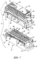
- FIGURE 1 is an enlarged fragmentary perspective view of the electrical connector assembly of the present invention with the receptacle and pin header members exploded from one another.
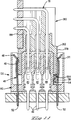
- FIGURE 2 is a cross sectional view of the connector assembly of the invention with the members exploded from each other.
- FIGURE 3 is a cross sectional view of the mated connector assembly with the members mated.
- FIGURE 4 is an enlarged fragmentary portion of an alternate embodiment of the receptacle member with a shunt terminal exploded therefrom.
- FIGURE 5 is enlarged portion of the receptacle member of Figure 4 illustrating the means for securing a shunt terminal to the housing sidewall.
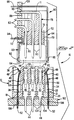
- FIGURE 6 is a fragmentary portion of the pin header member of the present invention with one of the ground plate shields exploded therefrom.
- FIGURE 7 is an enlarged fragmentary portion of Figure 6 illustrating the means for securing the ground plate to the pin header.
- FIGURE 8 is fragmentary perspective view of an alternative embodiment of the pin header for use with the receptacle member of Figure 4.
- FIGURE 9 is a cross sectional view of the receptacle member of Figure 4 mated with the pin header of Figure 8.
- FIGURE 10 is fragmentary perspective view of a pin header illustrating an alternate embodiment of the invention.
- FIGURE 11 is a cross sectional view of the receptacle of the present invention mated to an unshielded pin header member.
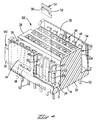
- FIGURE 12 is an exploded perspective view of a further alternative embodiment of the receptacle member.
- FIGURES 13 and 14 are enlarged views of portions of the receptacle member of Figure 12.
- FIGURE 15 is a cross sectional view of the assembled receptacle member of Figure 12.
- the connector assembly 10 of the present invention comprises a receptacle member 12 and a pin header 60.
- the board to board connector assembly 10 is shown in a configuration suitable for mounting daughter cards perpendicular to the mother board or backplane. It is to be understood that the pin header member can be modified for positioning the daughter cards in parallel with the mother board.
- Receptacle member 12 includes a housing member 14 having a mating face 16 and a mounting face 18. Housing 14 has a transverse body section 20 extending along the mounting face 18 as best seen in Figure 4, an inner body portion 22 and opposed outer side walls 34 extending from mounting face 18 to mating face 16 and defining elongate cavities 36 between the inner body portion 22 and respective outer side walls 34.
- Inner body portion 22 includes opposed side walls 24, end walls 28 having mounting flanges 30 extending outwardly therefrom, and a plurality of terminal-receiving passageways 32 extending from the mounting face 18 to the mating face 16.
- a plurality of first contact terminal members 40 are disposed in respective passageways 32, as shown in Figures 2 and 3. For purposes of illustration, first terminal members 40 have been eliminated in Figures 1 and 4.
- First terminal members 40 include a first contact section 42 for mating with complementary terminal members 78 of pin header 60 and a second contact section 44 extending below the mounting face 18 for engagement with corresponding apertures 104 of the circuit board 102.
- elongate cavities 36 are defined along thin sides by the inner surface of outer side walls 34 and the corresponding outer surfaces of body side walls 24 and the respective portions of transverse wall 20 extending therebetween forms cavity base 21.
- Cavity base 21 includes a plurality of apertures 38 extending therethrough.
- Receptacle 12 further includes a plurality of second contact terminal members 46 disposed in terminal-receiving apertures 38 of transverse wall 20 and having first contact sections 48 extending into elongate cavities 36 and a second contact section 52 extending outwardly from mounting face 18 for engagement with apertures 106 of mother board or backplane 102.
- first terminal section 48 of respective second contact terminals 46 include cantilevered beam portions having an inwardly directed arcuate section 49 and a contact surface 50 intermediate arcuate section 49 and second contact section 52.
- Corresponding contact surfaces 50 of second terminal members 46 are adapted to mate with corresponding ground bus means 84,90 of the complementary mating connector 60 as shown in Figure 3.
- FIGS 4 and 5 illustrate an alternative receptacle member embodiment 120, which includes at least one shunt terminal member 54 to provide an internal "switching effect.” Since the basic structure of receptacle member 120 is essentially the same as that of receptacle member 12, the same reference numerals have been used for the identical parts.
- Receptacle member 120 includes a housing member 140 having a transverse body section 20 extending along the mounting face 18 as best seen in Figure 4, an inner body portion 122 and opposed outer side walls 34 extending upward from the mounting face 18 and defining elongate cavities 36 between the inner body portion 122 and respective outer side walls 34.
- Inner body portion 122 includes opposed side walls 124, end walls 28 having mounting flanges 30 extending outwardly therefrom.
- the outside surfaces of side walls 124 of inner body portion 122 further include projections 126 extending into respective cavities 36 at selected locations therealong.
- Projections 126 include slots 127 for receiving a shunt terminal member 54 therebetween.
- Shunt terminal member 54 includes an outwardly extending portion 56 and ends 58, the ends 58 being received in projection slots 127 and extending between two adjacent second terminal members 46.
- shunt terminal member 54 electrically interconnects two adjacent second terminal members 46 within a respective cavity 36, when the receptacle member 120 is not mated to a complementary connector.
- the pin header 60 of the present invention includes a housing 62 having a mating face 64 and mounting face 68. Cavity 66, configured to receive inner housing 22 of mating receptacle 12 therein, extends inwardly from mating face 64.
- pin header 60 is shown in a right angle configuration for mounting to a daughter card 108.
- Pin header 60 includes side wall 70 opposed to mounting face 68, back wall 71 opposed to mating face 64, and opposed end walls 72 having outwardly extending flanges 74 thereon.
- Housing 62 further includes a plurality of terminal-receiving passageways 76 extending through the housing 62 and between the mating and mounting faces 64,68.
- a plurality of third terminal members 78 having first and second contact sections 80,82 are disposed within respective terminal-receiving passageways 76.
- the terminal-receiving passageways 76 include slots 77 along the back wall 71 for assembling respective third terminal members 78 into the housing 62.
- First contact section 80 of each third terminal member 78 is shown as a pin member adapted for mating with a complementary first terminal member 40 and second contact section is adapted for mounting to corresponding apertures 110 of daughter card 108.
- Pin header 60 further includes first and second ground or shield plate means 84,90 disposed on outer surfaces of the connector with first ground plate means 84 extending along back wall 71 and side wall 70.
- the first ground plate 84 includes first and second connecting portions 86,88 respectively, the first ground connecting portion 86 being adapted for electrical connection with the second terminal members 46 in one of the cavities 36 of receptacle 12, as best seen in Figure 3.
- the second ground plate 90 extends along the forwardly projecting portion of mounting face 68 of pin header 60 and is adapted to be received within the other of the elongate cavities 36 of the corresponding receptacle member 12 and to be electrically engaged to the plurality of second contact members 46 therein.
- the ground plate members 84 and 90 include outwardly extending tabs 85,91 for being received into corresponding slots 75 in the outwardly extending flanges 74 to secure the ground plates 84,90 continuously along the corresponding sides of the housing member 62.
- Figures 8 and 9 illustrate alternative pin header embodiment 160 for mating with receptacle member 120 of Figure 4 having at least one shunt terminal member 54 disposed along a side wall 124.
- wall 170 of pin header housing member 162 includes at least one projection 171 extending outwardly therefrom at a location selected to correspond to the location of the shunt terminal member 54 of receptacle member 120 of Figure 4.
- First plate member 184 includes at least one slot 187 extending thereinto from the edge of the first contact portion 186 at a location selected to correspond to the location of shunt terminal member 54 of receptacle member 120.
- Figure 10 shows a further alternative pin header embodiment 260 wherein first plate member 284 includes a plurality of segments 285, each including at least one aperture 287 therein for cooperating with projection means 271 on a wall 270 of pin header housing member 262.
- Wall 270 further includes a plurality of spacer members 273, which aid in keeping shield segments 285 from rotating.
- plate segments 285 are heat staked to the housing wall. Only the second corresponding receptacle terminal members 46 (as shown in Figure 1) associated with each individual segment 285 are commoned. By using a plurality of plate segments the individual segments can be used for interconnection of either signal, ground or power circuits, thereby increasing the capability of the connector assembly.
- the receptacle 12 of the present invention is intermatable with an unshielded pin header 160 as well as the grounded or shielded pin header 60 of the present invention.
- the arcuate portion 49 of each of the second terminal members 46 engage the outer surface of dielectric housing 162.
- the electrical contact region 50 of receptacle member 12 is, therefore, protected from accumulating films or debris from the dielectric housing walls of the unshielded pin header 160.
- the same receptacle member 12 can be mated interchangeably with a shielded or grounded pin header or unshielded pin header 60,160. Any buildup of dielectric material on the second contact terminal 46 occurs at the arcuate portion 49 rather than the contact section 50.
- FIGS 12-15 illustrate another alternative receptacle embodiment 412 wherein the housing means is comprised of first and second housing members 414a and 414b, which together define elongate cavities 436 extending between corresponding sides 424 and 434 of first and second housing members 414a,414b respectively, as best seen in Figure 15.
- Housing members 414a and 414b are securable together along their respective longitudinal sides by respective interlocking "teeth" 426,435 and at the ends by interlocking teeth and groves, 431a,431b.
- First housing member 414a corresponds to the inner housing portion of the previously described embodiments and includes mating face 416, mounting face 418, side walls 424 and end walls 428.
- a plurality of spaced outwardly projecting teeth 426 extend along the outer surface of wall 424 proximate mounting face 418.
- a plurality of first terminal members 440 having first and second connecting portions 442,444, respectively are disposed in respective terminal-receiving passageways 432.
- Second housing member 414b is essentially a shell member having longitudinally extending side walls 434, end walls 433, and a plurality of terminal-receiving passageways 438 for receiving second terminal members 446 therein.
- Second terminal members 446 include first contact section 448 having an arcuate portion 449 adjacent free end 447 and second contact section 452 extending through lower second housing wall 421.
- FIG. 15 The assembled receptacle 412 having a shunt terminal member 454 is shown in Figure 15.
- Figures 13 and 14 show enlarged views of the respective interlocked walls 424,434 at a shunt location.
- Selected teeth 426 along wall 424 are provided with slots 427 for receiving ends of shunt terminal members 454 in a manner similar to that previously described.
- Housing wall 424 as shown in Figure 14, includes two such teeth 426 having a shunt terminal 454 disposed therebetween. Tooth 426a intermediate the modified teeth 426 has been shortened to accommodate the outwardly projecting contact surface 456 of shunt terminal 454.
- the inner surfaces of wall 434 includes teeth 435 that are adopted to interlock with first housing member teeth 426 to secure the first and second housings together. This figure also shows the shortening of two of the teeth 435a at a shunt terminal location to accommodate the shape of the shunt terminal.
- the housing members of the present invention are molded from a suitable dielectric material such as a glass-filled polyester or the like.
- the first and second terminal members are from a material having high spring characteristics such as stamped and formed phosphor bronze or the like. Since the third terminal members are not spring members they may be formed of brass or other suitable materials.
- Ground shields or plate members 84,90 are preferably made from a high conductivity brass.
- the shunt terminal members are made from beryllium copper.
- Second terminal members are inserted into terminal-receiving passageways from the mating face and are secured therein as known in the art. If desired, shunt contact are inserted at the appropriate locations along the housing sidewalls.
- the receptacle of Figures 12-15 is assembled by loading the first and second terminals into their respective terminal-receiving passageways and any shunt contacts into their respective locations.
- the two housing members are assembled by engaging the teeth along the sidewalls and sliding the members together.
- the assembled receptacle member can then be mounted to a board 102 by inserting respective second contact sections of the first and second terminal members into corresponding board apertures and are held thereon by appropriate means.
- Pin header 60 is assembled by inserting third terminal members 78 into slots 77 along wall 70 of housing 62.
- the first and second ground plates 84,90 are assembled to housing 62 by inserting respective 85,91 into associated slots 75 to flanges 74.
- the plate members 84,90 it is preferable to include a plurality of second contact sections 84,90 respectively thereby providing multiple parallel paths to ground, thus lowering the inductance and resistance to ground.
- the number of outwardly extending second ground contact sections 88,94 of the plates 84,90 correspond to the number of columns of third terminal members 68 in the pin header 60 and the corresponding second terminal members 46 of the receptacle member 12 correspond to the columns of first terminal members 40 within the receptacle housing 14.
- the present invention provides a number of advantages for board to board connector systems. As is shown in the drawings a connector system is compatible with existing ungrounded/shielded connectors thereby permitting the user to gradually upgrade the system. Since the configuration of the basic pin header and basic receptacle member remains the same, both the enhanced and the standard pin header and receptacle member can be used interchangeably.
Landscapes
- Details Of Connecting Devices For Male And Female Coupling (AREA)
- Coupling Device And Connection With Printed Circuit (AREA)
- Connector Housings Or Holding Contact Members (AREA)
Applications Claiming Priority (2)
| Application Number | Priority Date | Filing Date | Title |
|---|---|---|---|
| US58636090A | 1990-09-21 | 1990-09-21 | |
| US586360 | 1990-09-21 |
Publications (4)
| Publication Number | Publication Date |
|---|---|
| EP0476883A2 true EP0476883A2 (de) | 1992-03-25 |
| EP0476883A3 EP0476883A3 (en) | 1992-10-14 |
| EP0476883B1 EP0476883B1 (de) | 1995-10-25 |
| EP0476883B2 EP0476883B2 (de) | 2000-12-20 |
Family
ID=24345430
Family Applications (1)
| Application Number | Title | Priority Date | Filing Date |
|---|---|---|---|
| EP91308042A Expired - Lifetime EP0476883B2 (de) | 1990-09-21 | 1991-08-30 | Elektrische Steckverbinderanordnung |
Country Status (4)
| Country | Link |
|---|---|
| EP (1) | EP0476883B2 (de) |
| JP (1) | JP3194603B2 (de) |
| KR (1) | KR970004153B1 (de) |
| DE (1) | DE69114094T2 (de) |
Cited By (8)
| Publication number | Priority date | Publication date | Assignee | Title |
|---|---|---|---|---|
| FR2707046A1 (de) * | 1993-04-05 | 1994-12-30 | Teradyne Inc | |
| EP0540310B1 (de) * | 1991-11-01 | 1996-07-03 | The Whitaker Corporation | Elektrischer Verbinder mit aussenseitig befestigten Erdpotentialschichten |
| US5605476A (en) * | 1993-04-05 | 1997-02-25 | Teradyne, Inc. | Shielded electrical connector |
| DE19640847A1 (de) * | 1996-10-03 | 1998-04-09 | Amp Holland | Rechtwinkliger abgeschirmter elektrischer Verbinder |
| WO1999003173A1 (en) * | 1997-07-10 | 1999-01-21 | The Whitaker Corporation | Apparatus for forming a connection through a board |
| EP0884809A3 (de) * | 1997-06-13 | 2000-04-26 | Sumitomo Wiring Systems, Ltd. | Steckverbinder für Leiterplatte |
| WO2001050551A1 (en) * | 1999-12-30 | 2001-07-12 | Lexel A/S | An electrical circuit board and a multiconnector |
| CN114421241A (zh) * | 2022-01-26 | 2022-04-29 | 成电智连(成都)科技有限公司 | 电连接器以及电连接器组件 |
Families Citing this family (3)
| Publication number | Priority date | Publication date | Assignee | Title |
|---|---|---|---|---|
| JP4669824B2 (ja) * | 2006-08-07 | 2011-04-13 | 任天堂株式会社 | コネクタ |
| DE102011006934A1 (de) * | 2011-04-07 | 2012-10-11 | Robert Bosch Gmbh | Elektrische Steckvorrichtung mit voreilender Kontaktierung |
| JP6140473B2 (ja) * | 2013-02-27 | 2017-05-31 | 矢崎総業株式会社 | シールドコネクタ及びシールドコネクタ接続構造 |
Family Cites Families (4)
| Publication number | Priority date | Publication date | Assignee | Title |
|---|---|---|---|---|
| US4869677A (en) * | 1984-08-17 | 1989-09-26 | Teradyne, Inc. | Backplane connector |
| US4601527A (en) * | 1985-01-18 | 1986-07-22 | E. I. Du Pont De Nemours And Company | Shielded header and cable assembly |
| EP0273589B1 (de) * | 1986-12-22 | 1993-09-01 | The Whitaker Corporation | Coaxial-Steckverbinder mit hoher Dichte |
| US4867690A (en) * | 1988-06-17 | 1989-09-19 | Amp Incorporated | Electrical connector system |
-
1991
- 1991-08-30 DE DE69114094T patent/DE69114094T2/de not_active Expired - Lifetime
- 1991-08-30 EP EP91308042A patent/EP0476883B2/de not_active Expired - Lifetime
- 1991-09-16 KR KR1019910016084A patent/KR970004153B1/ko not_active Expired - Lifetime
- 1991-09-20 JP JP26863891A patent/JP3194603B2/ja not_active Expired - Lifetime
Cited By (11)
| Publication number | Priority date | Publication date | Assignee | Title |
|---|---|---|---|---|
| EP0540310B1 (de) * | 1991-11-01 | 1996-07-03 | The Whitaker Corporation | Elektrischer Verbinder mit aussenseitig befestigten Erdpotentialschichten |
| FR2707046A1 (de) * | 1993-04-05 | 1994-12-30 | Teradyne Inc | |
| US5605476A (en) * | 1993-04-05 | 1997-02-25 | Teradyne, Inc. | Shielded electrical connector |
| US5607326A (en) * | 1993-04-05 | 1997-03-04 | Teradyne, Inc. | Shielded electrical connector |
| DE19640847A1 (de) * | 1996-10-03 | 1998-04-09 | Amp Holland | Rechtwinkliger abgeschirmter elektrischer Verbinder |
| DE19640847B4 (de) * | 1996-10-03 | 2007-03-08 | Amp-Holland B.V. | Rechtwinkliger abgeschirmter elektrischer Verbinder |
| EP0884809A3 (de) * | 1997-06-13 | 2000-04-26 | Sumitomo Wiring Systems, Ltd. | Steckverbinder für Leiterplatte |
| WO1999003173A1 (en) * | 1997-07-10 | 1999-01-21 | The Whitaker Corporation | Apparatus for forming a connection through a board |
| WO2001050551A1 (en) * | 1999-12-30 | 2001-07-12 | Lexel A/S | An electrical circuit board and a multiconnector |
| CN114421241A (zh) * | 2022-01-26 | 2022-04-29 | 成电智连(成都)科技有限公司 | 电连接器以及电连接器组件 |
| CN114421241B (zh) * | 2022-01-26 | 2024-04-30 | 成电智连(成都)科技有限公司 | 电连接器以及电连接器组件 |
Also Published As
| Publication number | Publication date |
|---|---|
| EP0476883B1 (de) | 1995-10-25 |
| KR970004153B1 (ko) | 1997-03-25 |
| KR920007264A (ko) | 1992-04-28 |
| EP0476883B2 (de) | 2000-12-20 |
| EP0476883A3 (en) | 1992-10-14 |
| JP3194603B2 (ja) | 2001-07-30 |
| DE69114094T2 (de) | 1996-05-30 |
| DE69114094D1 (de) | 1995-11-30 |
| JPH04255678A (ja) | 1992-09-10 |
Similar Documents
| Publication | Publication Date | Title |
|---|---|---|
| US5104329A (en) | Electrical connector assembly | |
| EP0460976B1 (de) | Steckverbinder mit Erdungsstruktur | |
| US6435914B1 (en) | Electrical connector having improved shielding means | |
| EP0829930B1 (de) | Elektrischer Steckverbinder mit integrierten Leistungsanschlüssen | |
| EP0405454B1 (de) | Koaxiales Kontaktelement | |
| US5135405A (en) | Connectors with ground structure | |
| CA2181316C (en) | Ic card connector shield grounding | |
| CA2166670C (en) | Shielded compact data connector | |
| EP0658953B1 (de) | Anordnung von modularen Steckern mit einer Mehrzahl von Öffnungen | |
| US5133679A (en) | Connectors with ground structure | |
| US4975084A (en) | Electrical connector system | |
| US6705902B1 (en) | Connector assembly having contacts with uniform electrical property of resistance | |
| US7976321B2 (en) | Electrical connector with a ground terminal | |
| US5486115A (en) | Connector assembly | |
| EP0365179B1 (de) | Elektrisches Verbindersystem | |
| EP0476883B2 (de) | Elektrische Steckverbinderanordnung | |
| US6296518B1 (en) | Stacked electrical connector assembly | |
| US5174771A (en) | Electrical connector having externally mounted ground plates | |
| US20250385468A1 (en) | Electrical connector assembly with an improved mating interface | |
| EP0540310B1 (de) | Elektrischer Verbinder mit aussenseitig befestigten Erdpotentialschichten | |
| HK1012782A1 (en) | High speed guarded cavity backplane connector |
Legal Events
| Date | Code | Title | Description |
|---|---|---|---|
| PUAI | Public reference made under article 153(3) epc to a published international application that has entered the european phase |
Free format text: ORIGINAL CODE: 0009012 |
|
| AK | Designated contracting states |
Kind code of ref document: A2 Designated state(s): DE FR GB IT NL |
|
| PUAL | Search report despatched |
Free format text: ORIGINAL CODE: 0009013 |
|
| AK | Designated contracting states |
Kind code of ref document: A3 Designated state(s): DE FR GB IT NL |
|
| RAP1 | Party data changed (applicant data changed or rights of an application transferred) |
Owner name: THE WHITAKER CORPORATION |
|
| 17P | Request for examination filed |
Effective date: 19930402 |
|
| 17Q | First examination report despatched |
Effective date: 19941012 |
|
| GRAA | (expected) grant |
Free format text: ORIGINAL CODE: 0009210 |
|
| AK | Designated contracting states |
Kind code of ref document: B1 Designated state(s): DE FR GB IT NL |
|
| ITF | It: translation for a ep patent filed | ||
| REF | Corresponds to: |
Ref document number: 69114094 Country of ref document: DE Date of ref document: 19951130 |
|
| ET | Fr: translation filed | ||
| PLBI | Opposition filed |
Free format text: ORIGINAL CODE: 0009260 |
|
| PLBF | Reply of patent proprietor to notice(s) of opposition |
Free format text: ORIGINAL CODE: EPIDOS OBSO |
|
| 26 | Opposition filed |
Opponent name: SIEMENS AG GR PA 6 Effective date: 19960725 |
|
| NLR1 | Nl: opposition has been filed with the epo |
Opponent name: SIEMENS AG GR PA 6 |
|
| PLBF | Reply of patent proprietor to notice(s) of opposition |
Free format text: ORIGINAL CODE: EPIDOS OBSO |
|
| PLBF | Reply of patent proprietor to notice(s) of opposition |
Free format text: ORIGINAL CODE: EPIDOS OBSO |
|
| PLBF | Reply of patent proprietor to notice(s) of opposition |
Free format text: ORIGINAL CODE: EPIDOS OBSO |
|
| PLAW | Interlocutory decision in opposition |
Free format text: ORIGINAL CODE: EPIDOS IDOP |
|
| APAC | Appeal dossier modified |
Free format text: ORIGINAL CODE: EPIDOS NOAPO |
|
| APAE | Appeal reference modified |
Free format text: ORIGINAL CODE: EPIDOS REFNO |
|
| APAC | Appeal dossier modified |
Free format text: ORIGINAL CODE: EPIDOS NOAPO |
|
| PLBQ | Unpublished change to opponent data |
Free format text: ORIGINAL CODE: EPIDOS OPPO |
|
| PLAB | Opposition data, opponent's data or that of the opponent's representative modified |
Free format text: ORIGINAL CODE: 0009299OPPO |
|
| R26 | Opposition filed (corrected) |
Opponent name: SIEMENS AG GR PA 6 Effective date: 19960725 |
|
| APAC | Appeal dossier modified |
Free format text: ORIGINAL CODE: EPIDOS NOAPO |
|
| NLR1 | Nl: opposition has been filed with the epo |
Opponent name: SIEMENS AG GR PA 6 |
|
| PLAW | Interlocutory decision in opposition |
Free format text: ORIGINAL CODE: EPIDOS IDOP |
|
| PUAH | Patent maintained in amended form |
Free format text: ORIGINAL CODE: 0009272 |
|
| STAA | Information on the status of an ep patent application or granted ep patent |
Free format text: STATUS: PATENT MAINTAINED AS AMENDED |
|
| 27A | Patent maintained in amended form |
Effective date: 20001220 |
|
| AK | Designated contracting states |
Kind code of ref document: B2 Designated state(s): DE FR GB IT NL |
|
| RIC2 | Information provided on ipc code assigned after grant |
Free format text: 7H 01R 13/658 A, 7H 01R 12/18 B, 7H 01R 12/20 B |
|
| ITF | It: translation for a ep patent filed | ||
| NLR2 | Nl: decision of opposition | ||
| NLR3 | Nl: receipt of modified translations in the netherlands language after an opposition procedure | ||
| ET3 | Fr: translation filed ** decision concerning opposition | ||
| REG | Reference to a national code |
Ref country code: GB Ref legal event code: IF02 |
|
| APAH | Appeal reference modified |
Free format text: ORIGINAL CODE: EPIDOSCREFNO |
|
| PGFP | Annual fee paid to national office [announced via postgrant information from national office to epo] |
Ref country code: NL Payment date: 20100824 Year of fee payment: 20 |
|
| PGFP | Annual fee paid to national office [announced via postgrant information from national office to epo] |
Ref country code: FR Payment date: 20100831 Year of fee payment: 20 Ref country code: DE Payment date: 20100827 Year of fee payment: 20 Ref country code: IT Payment date: 20100826 Year of fee payment: 20 |
|
| PGFP | Annual fee paid to national office [announced via postgrant information from national office to epo] |
Ref country code: GB Payment date: 20100825 Year of fee payment: 20 |
|
| REG | Reference to a national code |
Ref country code: DE Ref legal event code: R071 Ref document number: 69114094 Country of ref document: DE |
|
| REG | Reference to a national code |
Ref country code: DE Ref legal event code: R071 Ref document number: 69114094 Country of ref document: DE |
|
| REG | Reference to a national code |
Ref country code: NL Ref legal event code: V4 Effective date: 20110830 |
|
| REG | Reference to a national code |
Ref country code: GB Ref legal event code: PE20 Expiry date: 20110829 |
|
| PG25 | Lapsed in a contracting state [announced via postgrant information from national office to epo] |
Ref country code: GB Free format text: LAPSE BECAUSE OF EXPIRATION OF PROTECTION Effective date: 20110829 |
|
| PG25 | Lapsed in a contracting state [announced via postgrant information from national office to epo] |
Ref country code: NL Free format text: LAPSE BECAUSE OF EXPIRATION OF PROTECTION Effective date: 20110830 |
|
| PG25 | Lapsed in a contracting state [announced via postgrant information from national office to epo] |
Ref country code: DE Free format text: LAPSE BECAUSE OF EXPIRATION OF PROTECTION Effective date: 20110831 |