EP0477566B1 - Verbesserungen für oder bezüglich der Lichtmodulation - Google Patents
Verbesserungen für oder bezüglich der Lichtmodulation Download PDFInfo
- Publication number
- EP0477566B1 EP0477566B1 EP91114435A EP91114435A EP0477566B1 EP 0477566 B1 EP0477566 B1 EP 0477566B1 EP 91114435 A EP91114435 A EP 91114435A EP 91114435 A EP91114435 A EP 91114435A EP 0477566 B1 EP0477566 B1 EP 0477566B1
- Authority
- EP
- European Patent Office
- Prior art keywords
- modulation
- modulating
- elements
- modulating elements
- amplitude
- Prior art date
- Legal status (The legal status is an assumption and is not a legal conclusion. Google has not performed a legal analysis and makes no representation as to the accuracy of the status listed.)
- Expired - Lifetime
Links
- 238000000034 method Methods 0.000 claims description 20
- 230000003287 optical effect Effects 0.000 claims description 16
- 125000006850 spacer group Chemical group 0.000 claims description 8
- 239000000758 substrate Substances 0.000 claims description 5
- 230000004913 activation Effects 0.000 claims description 4
- 238000006073 displacement reaction Methods 0.000 claims description 2
- 238000009826 distribution Methods 0.000 description 6
- 230000008569 process Effects 0.000 description 6
- 238000004458 analytical method Methods 0.000 description 3
- 239000004973 liquid crystal related substance Substances 0.000 description 3
- 230000004044 response Effects 0.000 description 3
- 230000008901 benefit Effects 0.000 description 2
- 230000008859 change Effects 0.000 description 2
- 230000010354 integration Effects 0.000 description 2
- 238000003491 array Methods 0.000 description 1
- 230000001427 coherent effect Effects 0.000 description 1
- 230000005684 electric field Effects 0.000 description 1
- 230000010365 information processing Effects 0.000 description 1
- 230000010287 polarization Effects 0.000 description 1
Images

Classifications
-
- G—PHYSICS
- G02—OPTICS
- G02F—OPTICAL DEVICES OR ARRANGEMENTS FOR THE CONTROL OF LIGHT BY MODIFICATION OF THE OPTICAL PROPERTIES OF THE MEDIA OF THE ELEMENTS INVOLVED THEREIN; NON-LINEAR OPTICS; FREQUENCY-CHANGING OF LIGHT; OPTICAL LOGIC ELEMENTS; OPTICAL ANALOGUE/DIGITAL CONVERTERS
- G02F2/00—Demodulating light; Transferring the modulation of modulated light; Frequency-changing of light
-
- G—PHYSICS
- G09—EDUCATION; CRYPTOGRAPHY; DISPLAY; ADVERTISING; SEALS
- G09G—ARRANGEMENTS OR CIRCUITS FOR CONTROL OF INDICATING DEVICES USING STATIC MEANS TO PRESENT VARIABLE INFORMATION
- G09G3/00—Control arrangements or circuits, of interest only in connection with visual indicators other than cathode-ray tubes
- G09G3/20—Control arrangements or circuits, of interest only in connection with visual indicators other than cathode-ray tubes for presentation of an assembly of a number of characters, e.g. a page, by composing the assembly by combination of individual elements arranged in a matrix no fixed position being assigned to or needed to be assigned to the individual characters or partial characters
- G09G3/34—Control arrangements or circuits, of interest only in connection with visual indicators other than cathode-ray tubes for presentation of an assembly of a number of characters, e.g. a page, by composing the assembly by combination of individual elements arranged in a matrix no fixed position being assigned to or needed to be assigned to the individual characters or partial characters by control of light from an independent source
- G09G3/3433—Control arrangements or circuits, of interest only in connection with visual indicators other than cathode-ray tubes for presentation of an assembly of a number of characters, e.g. a page, by composing the assembly by combination of individual elements arranged in a matrix no fixed position being assigned to or needed to be assigned to the individual characters or partial characters by control of light from an independent source using light modulating elements actuated by an electric field and being other than liquid crystal devices and electrochromic devices
- G09G3/346—Control arrangements or circuits, of interest only in connection with visual indicators other than cathode-ray tubes for presentation of an assembly of a number of characters, e.g. a page, by composing the assembly by combination of individual elements arranged in a matrix no fixed position being assigned to or needed to be assigned to the individual characters or partial characters by control of light from an independent source using light modulating elements actuated by an electric field and being other than liquid crystal devices and electrochromic devices based on modulation of the reflection angle, e.g. micromirrors
-
- G—PHYSICS
- G02—OPTICS
- G02B—OPTICAL ELEMENTS, SYSTEMS OR APPARATUS
- G02B26/00—Optical devices or arrangements for the control of light using movable or deformable optical elements
- G02B26/001—Optical devices or arrangements for the control of light using movable or deformable optical elements based on interference in an adjustable optical cavity
-
- G—PHYSICS
- G02—OPTICS
- G02B—OPTICAL ELEMENTS, SYSTEMS OR APPARATUS
- G02B26/00—Optical devices or arrangements for the control of light using movable or deformable optical elements
- G02B26/06—Optical devices or arrangements for the control of light using movable or deformable optical elements for controlling the phase of light
-
- G—PHYSICS
- G02—OPTICS
- G02B—OPTICAL ELEMENTS, SYSTEMS OR APPARATUS
- G02B26/00—Optical devices or arrangements for the control of light using movable or deformable optical elements
- G02B26/08—Optical devices or arrangements for the control of light using movable or deformable optical elements for controlling the direction of light
- G02B26/0816—Optical devices or arrangements for the control of light using movable or deformable optical elements for controlling the direction of light by means of one or more reflecting elements
- G02B26/0833—Optical devices or arrangements for the control of light using movable or deformable optical elements for controlling the direction of light by means of one or more reflecting elements the reflecting element being a micromechanical device, e.g. a MEMS mirror, DMD
- G02B26/0841—Optical devices or arrangements for the control of light using movable or deformable optical elements for controlling the direction of light by means of one or more reflecting elements the reflecting element being a micromechanical device, e.g. a MEMS mirror, DMD the reflecting element being moved or deformed by electrostatic means
-
- G—PHYSICS
- G09—EDUCATION; CRYPTOGRAPHY; DISPLAY; ADVERTISING; SEALS
- G09F—DISPLAYING; ADVERTISING; SIGNS; LABELS OR NAME-PLATES; SEALS
- G09F9/00—Indicating arrangements for variable information in which the information is built-up on a support by selection or combination of individual elements
- G09F9/30—Indicating arrangements for variable information in which the information is built-up on a support by selection or combination of individual elements in which the desired character or characters are formed by combining individual elements
- G09F9/37—Indicating arrangements for variable information in which the information is built-up on a support by selection or combination of individual elements in which the desired character or characters are formed by combining individual elements being movable elements
- G09F9/372—Indicating arrangements for variable information in which the information is built-up on a support by selection or combination of individual elements in which the desired character or characters are formed by combining individual elements being movable elements the positions of the elements being controlled by the application of an electric field
-
- G—PHYSICS
- G09—EDUCATION; CRYPTOGRAPHY; DISPLAY; ADVERTISING; SEALS
- G09G—ARRANGEMENTS OR CIRCUITS FOR CONTROL OF INDICATING DEVICES USING STATIC MEANS TO PRESENT VARIABLE INFORMATION
- G09G2300/00—Aspects of the constitution of display devices
- G09G2300/04—Structural and physical details of display devices
- G09G2300/0439—Pixel structures
- G09G2300/0443—Pixel structures with several sub-pixels for the same colour in a pixel, not specifically used to display gradations
Definitions
- the present invention relates to methods of light modulation and spatial light modulators, including phase modulators and full complex light modulators.
- Spatial light modulators are devices used to control the distribution of light in an optical system. Spatial light modulators are divided into one- or two-dimensional arrays of modulation elements called pixels, or picture elements, that represent the smallest addressable unit within the device. The SLM pixel is used to modify either the amplitude or the phase of the light distribution within the optical system.
- the light modulation characteristics of most prior art SLMs are coupled combinations of amplitude and phase changes.
- the modulation characteristic of a pixel is controlled by a single applied signal, either an electrical voltage, current or incident optical intensity level, so the amplitude and phase characteristics of the pixel can not be independently set.
- phase modulation is essential since most of the signal information is contained in the phase terms.
- the additional control of amplitude provides means for rejecting noise in the filter plane for improved system performance.
- phase modulation liquid crystal, photorefractive, magnetooptic, and deformable mirror. All have coupled phase and amplitude modulation characteristics.
- Liquid crystals allow for phase and amplitude modulation, but phase modulation has extremely narrow ranges for the electric fields applied for uniform realignment, making it hard to control. Amplitude modulation is also difficult since the nonuniform realignment causing the amplitude modulation also contributes to phase modulation, resulting in a phase-amplitude coupled modulation.
- Photorefractive modulators work for phase-only modulation only at extremely high voltages. Birefringence caused in nonuniform alignment produces amplitude modulation. But since photorefractive, like liquid crystal, modulates by a change in the refractive index, phase modulation accompanies amplitude modulation.
- Magnetooptic modulators produce a binary change in the polarization of light, but are hard to control in operation.
- Kast, et al. in their article in Applied Optics , 15 March 1989, describe a method for ternary operation of magnetooptic modulators, but it has a very limited range of amplitude- or phase-only modulations, none of which are independently controlled.
- phase-only modulation Two other methods of phase-only modulation have been used. The first method was introduced by Brown and Lohmann in Applied Optics , 1966. Their technique, detour phase, requires very tight system alignment and limited field-of-view for the phase encoding approximations to be valid. The second was introduced by Hansche, et al., in their article in Applied Optics , 15 November, 1989. Their approach allows for different amplitudes to be produced, but requires a lowered resolution in the optical system.
- a deflectable beam spatial light modulator which is formed of an array of pixels, each pixel individually addressable and containing at least one deflectable reflecting mirror element.
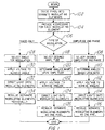
- a method of modulation of light using a spatial light modulator with a plurality of picture elements comprises the following steps:
- said addressing of said modulating elements consists of applying a predetermined voltage to an electrode located directly under said modulating element.
- the said modulation may be amplitude modulation or full complex modulation.
- a spatial light modulator in a second output thereof a spatial light modulator, comprises:
- said modulator is divided into two halves.
- said addressing circuitry includes a plurality of activation electrodes; one electrode corresponding to each modulating element.
- Full complex light modulation allows the modulation of a signal with independent control of phase and amplitude.
- the method described uses a standard picture element.
- the picture element is then divided into a number of smaller modulating elements.
- Each modulating element is provided with its own circuitry for addressing.
- the net phase angle, ⁇ , and the desired resultant amplitude, A must be selected.
- a and ⁇ a number of angles can be found. These angles, ⁇ 1 , ⁇ 2 , etc. are for the individual modulating elements.
- the addressing circuitry for the individual modulating elements is then activated in such a way as to cause the modulation at the angle ⁇ x .
- the light signal is then directed to the picture element and its individual modulating elements.
- the final step in the process occurs when the optical system scans the modulating elements and resolves them as if they were the whole picture element.
- the preferred embodiment shown uses a deformable mirror device (DMD) as the picture element.
- a flexure beam DMD is cut into a number, for example two, of smaller flexure beam DMDs.
- the addressing circuitry in this case is electrodes, which are located underneath each half of the picture element. The angles, ⁇ 1 , and ⁇ 2 , are caused when a voltage is applied to the electrodes. The value of the voltage applied determines the value of the angle.
- the preferred embodiment shows only two modulating elements but it is possible to use this method for more than two angles.
- step 102 the pixel is divided into however many modulating elements are desired within a pixel.
- step 104 provides for addressing circuitry for each modulating element within the pixel, so each is individually addressable.
- Step 106 is the point at which the type of modulation must be selected.
- step 108 If amplitude and phase modulation is desired, it is possible to perform both simultaneously. The process continues in this case to step 108.
- the desired amplitude, A, and net phase angle, ⁇ must be selected. Once those two variables are set, the angles for the individual modulating elements must be determined, in step 110.
- the complete analytical description of the optical distribution transmitted by, or reflected by, the full complex pixel is given by equation (1): where w x and w y are the widths of the modulating elements in the horizontal and vertical direction, W is the width of the entire square pixel region, and ⁇ 1 and ⁇ 2 are the phase setting of the individual modulators.
- Step 112 requires the application of the voltages in order to deflect the appropriate modulating elements to achieve the phase angles calculated in step 110.
- Step 114 is the part of the process that an actual optical signal is applied to the set elements by the system.
- Step 116 allows all of the independently addressed modulating elements to be integrated into one pixel.
- integration is the actual scanning done by the optical system, where the individual elements are grouped back into the original pixel. That is, the modulating elements, taken together are scanned by the optical system as though they were a single pixel.
- step 118 If amplitude-only modulation is desired, the process steps to 118.
- the modulated amplitude, A is selected.
- equations 6, 7, 8, and 9 it is possible to again solve for the individual angles, ⁇ 1 and ⁇ 2 , in step 120.
- the relationship for the voltage set out in equation 10 is again used to determine the amount of applied voltage necessary for the proper deflection and applied in step 122.
- Step 124 again requires the direction of light, and step 126 is the integration of the modulation elements into the original pixel.
- phase-only modulation is also possible.
- the process moves to step 128.
- the angle selected for phase modulation is the angle for the individual modulating elements.
- all individual modulating elements are set to that angle in step 130.
- each individual piece of the original pixel is treated as its own pixel. For example, if there existed an original array of N x N pixels, and each pixel was divided into two modulating elements, the system would scan an array of N x 2N pixels at step 134.
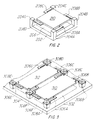
- FIGURE 2 shows a prior art configuration of a flexure beam DMD.
- An addressing electrode 206 is built onto a substrate 202.
- a mirror element 210 is built onto a spacer covering the layer containing 206. The spacer layer is then etched away. This leaves a layer of support posts 204A, 204B, 204C, and 204D, with an gap between the mirror element 210 and the electrode 206.
- a pre-determined voltage is applied to electrode 206, mirror element 210 is electrostatically attracted to it.
- the flexure hinges 208A, 208B, 208C, and 208D allow the mirror to deflect downwards. Because all four corners are supported, the mirror deflects with a piston-like movement.
- FIGURE 3 illustrates a divided DMD with two individual modulating elements. If a voltage is applied to address electrodes 302, then mirror 310 will deflect downwards flexing on hinges 306A, 306B, 306C, and 306F. Mirror 312 will not deflect unless a voltage is applied to address electrode 304, allowing independent operation of the two mirror elements. As in FIGURE 2, the flexure hinges 306A, 306B, 306C, 306D, 306E, and 306F, are supported by support posts 308A, 308B, 308C, 308D, 308E, and 308F, creating a gap between the mirror elements 310 and 312 and electrodes 302 and 304, respectively.
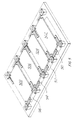
- the top view of the divided pixel is shown in FIGURE 4.
- the variables used in the above equations are shown.
- W x is along the horizontal axis, as indicated by the double-headed arrow 401, the distance from support post 402A to support post 402B.
- W y is along the vertical axis, indicated by the double-headed arrow 403, either from support post 402B to 402C, or from support post 402C to support post 402D.
- the pixel was divided horizontally into two parts, so there are two w y to one w x .
- Mirror elements 404 and 406 are individually addressable underneath the mirror surface, as seen in the perspective drawing of FIGURE 3.
- the preferred embodiment has w x equal to about 50 ⁇ m.
- W y would be about half of that, about 25 ⁇ m. Since w x is the same as the side length W, the active area of an undivided pixel in this case would be 2500 ⁇ m 2 . Due to loss of area from the gap between the two mirrors, support posts and hinges, the active area is actually about 2125 ⁇ m 2 . An advantage of this embodiment is that the divided pixel still has eighty-five percent of its original active area.
- FIGURE 5 shows an example of one possible other division of a pixel.
- the pixel is divided into two individual elements, which are in turn divided into two pieces.
- the mirror 502 has addressing electrode 510, and each other modulating element has a corresponding element, making all of them individually addressable.
- a feature of the present invention is that it may be applied to existing systems by replacing picture elements with divided picture elements in accordance with the present invention, for example prior art DMDs with divided DMDs.
- the optical arrangement of such existing system will inherently resolve such a divided pixel as a single picture atempt.
- full complex modulation capability may be added to the existing system.
Landscapes
- Physics & Mathematics (AREA)
- General Physics & Mathematics (AREA)
- Optics & Photonics (AREA)
- Engineering & Computer Science (AREA)
- Theoretical Computer Science (AREA)
- Computer Hardware Design (AREA)
- Spectroscopy & Molecular Physics (AREA)
- Nonlinear Science (AREA)
- Mechanical Light Control Or Optical Switches (AREA)
Claims (7)
- Verfahren zum Modulieren von Licht unter Verwendung eines räumlichen Lichtmodulators mit mehreren Bildelementen, enthaltend die folgenden Schritte:a) Aufteilen eines Bildelements in mehrere Modulationselemente (310, 312; 404, 406; 502, 504, 506, 508);b) Vorsehen einer Adressierungsschaltung für jedes der Modulationselemente (310, 312; 404, 406; 502, 504, 506, 508);c) Auswählen eines vorbestimmten Modulationsphasenwinkels und einer vorbestimmten Modulationsamplitude;d) Bestimmen geeigneter Verschiebungswinkel der Modulationselemente (310, 312; 404, 406; 502, 504, 506, 508), um den Phasenwinkel und die Amplitude zu erzielen;e) Adressieren der Modulationselemente (310, 312; 404, 406; 502, 504, 506, 508), um den vorbestimmten Phasenwinkel zu erzielen;f) Anordnen des räumlichen Lichtmodulators zum Auflösen der mehreren Modulationselemente (310, 312; 404, 406; 502, 504, 506, 508) als das Bildelement.
- Verfahren nach Anspruch 1, bei welchem:
a) das Adressieren der Modulationselemente (310, 312; 404, 406; 502, 504, 506, 508) darin besteht, eine vorbestimmte Spannung an eine Elektrode (302, 304; 510, 512, 514, 516) anzulegen, die sich direkt unter dem Modulationselement (310, 312; 404, 406; 502, 504, 506, 508) befindet. - Verfahren nach Anspruch 1 oder Anspruch 2, bei welchem die Modulation eine Amplitudenmodulation ist.
- Verfahren nach Anspruch 1 oder Anspruch 2, bei welchem die Modulation eine volle komplexe Modulation ist.
- Räumlicher Lichtmodulator, enthaltend:a) mehrere Bildelemente, die in einer Schichtstruktur gebildet sind, wobei jedes Bildelement in mehrere Modulationselemente (310, 312; 404, 406; 502, 504, 506, 508) aufgeteilt ist;b) wobei die Schichtstruktur ein Substrat, eine Abstandsschicht auf dem Substrat, eine Reflexionsschicht auf der Abstandsschicht und eine elektrische Adressierungsschaltung enthält;c) wobei jedes der mehreren Modulationselemente (310, 312; 404, 406; 502, 504, 506, 508) ein elektrostatisch ablenkbares Element ist, das in der Reflexionsschicht gebildet ist, und die Abstandsschicht (308A, 308B, 308C, 308D) eine Vertiefung zwischen dem ablenkbaren Element und mehreren Aktivierungselektroden bildet, die so angeordnet sind, daß sie die elektrostatische Ablenkung beeinflussen;d) wobei die elektrische Adressierungsschaltung derart ist, daß jedes der mehreren Modulationselemente (310, 312; 404, 406; 502, 504, 506, 508) unabhängig adressierbar ist; unde) ein optisches System, das eine solche Auflösung hat, daß jedes der mehreren Modulationselemente (310, 312; 404, 406; 502, 504, 506, 508) in das jedes Bildelement aufgeteilt ist, als ein Bildelement aufgelöst wird.
- Modulator nach Anspruch 5, bei welchem:
a) der Modulator in zwei Hälften aufgeteilt ist. - Modulator nach Anspruch 5 oder Anspruch 6, bei welchem:
a) die Adressierungsschaltung mehrere Aktivierungselektroden (310, 312) enthält, wobei eine Elektrode jeweils einem Modulationselement entspricht.
Applications Claiming Priority (2)
| Application Number | Priority Date | Filing Date | Title |
|---|---|---|---|
| US07/590,405 US5148157A (en) | 1990-09-28 | 1990-09-28 | Spatial light modulator with full complex light modulation capability |
| US590405 | 1990-09-28 |
Publications (3)
| Publication Number | Publication Date |
|---|---|
| EP0477566A2 EP0477566A2 (de) | 1992-04-01 |
| EP0477566A3 EP0477566A3 (en) | 1992-05-13 |
| EP0477566B1 true EP0477566B1 (de) | 1996-12-18 |
Family
ID=24362124
Family Applications (1)
| Application Number | Title | Priority Date | Filing Date |
|---|---|---|---|
| EP91114435A Expired - Lifetime EP0477566B1 (de) | 1990-09-28 | 1991-08-28 | Verbesserungen für oder bezüglich der Lichtmodulation |
Country Status (5)
| Country | Link |
|---|---|
| US (1) | US5148157A (de) |
| EP (1) | EP0477566B1 (de) |
| JP (1) | JP3155307B2 (de) |
| KR (1) | KR100231123B1 (de) |
| DE (1) | DE69123676T2 (de) |
Cited By (2)
| Publication number | Priority date | Publication date | Assignee | Title |
|---|---|---|---|---|
| DE102007051520A1 (de) | 2007-10-19 | 2009-04-23 | Seereal Technologies S.A. | Komplexwertiger räumlicher Lichtmodulator |
| CN100585674C (zh) * | 2004-08-27 | 2010-01-27 | Idc公司 | 用于寻址mems显示器的系统和方法 |
Families Citing this family (113)
| Publication number | Priority date | Publication date | Assignee | Title |
|---|---|---|---|---|
| US5083857A (en) * | 1990-06-29 | 1992-01-28 | Texas Instruments Incorporated | Multi-level deformable mirror device |
| GB9024979D0 (en) * | 1990-11-16 | 1991-01-02 | Rank Cintel Ltd | Digital mirror spatial light modulator |
| EP0539889A3 (en) * | 1991-10-30 | 1993-07-28 | Steinbichler, Hans, Dr. | Micromechanical actuator |
| US5312513A (en) * | 1992-04-03 | 1994-05-17 | Texas Instruments Incorporated | Methods of forming multiple phase light modulators |
| US6219015B1 (en) | 1992-04-28 | 2001-04-17 | The Board Of Directors Of The Leland Stanford, Junior University | Method and apparatus for using an array of grating light valves to produce multicolor optical images |
| US5416618A (en) * | 1992-11-10 | 1995-05-16 | The United States Of America As Represented By The Administrator Of The National Aeronautics & Space Administration | Full complex modulation using two one-parameter spatial light modulators |
| US6674562B1 (en) | 1994-05-05 | 2004-01-06 | Iridigm Display Corporation | Interferometric modulation of radiation |
| US5457493A (en) * | 1993-09-15 | 1995-10-10 | Texas Instruments Incorporated | Digital micro-mirror based image simulation system |
| EP0657760A1 (de) * | 1993-09-15 | 1995-06-14 | Texas Instruments Incorporated | Bildsimulations- und Projektionssystem |
| US6680792B2 (en) | 1994-05-05 | 2004-01-20 | Iridigm Display Corporation | Interferometric modulation of radiation |
| US7138984B1 (en) | 2001-06-05 | 2006-11-21 | Idc, Llc | Directly laminated touch sensitive screen |
| US7460291B2 (en) * | 1994-05-05 | 2008-12-02 | Idc, Llc | Separable modulator |
| US5793600A (en) * | 1994-05-16 | 1998-08-11 | Texas Instruments Incorporated | Method for forming high dielectric capacitor electrode structure and semiconductor memory devices |
| US5712912A (en) * | 1995-07-28 | 1998-01-27 | Mytec Technologies Inc. | Method and apparatus for securely handling a personal identification number or cryptographic key using biometric techniques |
| US6560018B1 (en) | 1994-10-27 | 2003-05-06 | Massachusetts Institute Of Technology | Illumination system for transmissive light valve displays |
| US5841579A (en) | 1995-06-07 | 1998-11-24 | Silicon Light Machines | Flat diffraction grating light valve |
| US5740276A (en) * | 1995-07-27 | 1998-04-14 | Mytec Technologies Inc. | Holographic method for encrypting and decrypting information using a fingerprint |
| US6525750B1 (en) | 1996-03-08 | 2003-02-25 | Duke University | Projection display for computers |
| US5768242A (en) * | 1996-04-05 | 1998-06-16 | The United States Of America As Representd By The Administrator Of The National Aeronautics And Space Administration | Apparatus and method for focusing a light beam in a three-dimensional recording medium by a dynamic holographic device |
| US5833360A (en) * | 1996-10-17 | 1998-11-10 | Compaq Computer Corporation | High efficiency lamp apparatus for producing a beam of polarized light |
| US6390626B2 (en) | 1996-10-17 | 2002-05-21 | Duke University | Image projection system engine assembly |
| US6243152B1 (en) | 1996-12-17 | 2001-06-05 | Duke University | Contrast polymer dispersed liquid crystal projection display system |
| US5868480A (en) * | 1996-12-17 | 1999-02-09 | Compaq Computer Corporation | Image projection apparatus for producing an image supplied by parallel transmitted colored light |
| US5977942A (en) * | 1996-12-20 | 1999-11-02 | Compaq Computer Corporation | Multiplexed display element sequential color LCD panel |
| US6313893B1 (en) | 1996-12-27 | 2001-11-06 | Duke University | Compensation for DC balancing of liquid crystal displays |
| US5982553A (en) | 1997-03-20 | 1999-11-09 | Silicon Light Machines | Display device incorporating one-dimensional grating light-valve array |
| CA2203212A1 (en) | 1997-04-21 | 1998-10-21 | Vijayakumar Bhagavatula | Methodology for biometric encryption |
| US5867251A (en) * | 1997-05-02 | 1999-02-02 | The General Hospital Corp. | Scanning ophthalmoscope with spatial light modulators |
| US5963367A (en) * | 1997-09-23 | 1999-10-05 | Lucent Technologies, Inc. | Micromechanical xyz stage for use with optical elements |
| US6088102A (en) | 1997-10-31 | 2000-07-11 | Silicon Light Machines | Display apparatus including grating light-valve array and interferometric optical system |
| US6816302B2 (en) | 1998-03-02 | 2004-11-09 | Micronic Laser Systems Ab | Pattern generator |
| SE9800665D0 (sv) | 1998-03-02 | 1998-03-02 | Micronic Laser Systems Ab | Improved method for projection printing using a micromirror SLM |
| US8928967B2 (en) | 1998-04-08 | 2015-01-06 | Qualcomm Mems Technologies, Inc. | Method and device for modulating light |
| KR100703140B1 (ko) | 1998-04-08 | 2007-04-05 | 이리다임 디스플레이 코포레이션 | 간섭 변조기 및 그 제조 방법 |
| US6271808B1 (en) | 1998-06-05 | 2001-08-07 | Silicon Light Machines | Stereo head mounted display using a single display device |
| US6130770A (en) | 1998-06-23 | 2000-10-10 | Silicon Light Machines | Electron gun activated grating light valve |
| US6101036A (en) | 1998-06-23 | 2000-08-08 | Silicon Light Machines | Embossed diffraction grating alone and in combination with changeable image display |
| US6215579B1 (en) | 1998-06-24 | 2001-04-10 | Silicon Light Machines | Method and apparatus for modulating an incident light beam for forming a two-dimensional image |
| US6303986B1 (en) | 1998-07-29 | 2001-10-16 | Silicon Light Machines | Method of and apparatus for sealing an hermetic lid to a semiconductor die |
| US6872984B1 (en) | 1998-07-29 | 2005-03-29 | Silicon Light Machines Corporation | Method of sealing a hermetic lid to a semiconductor die at an angle |
| US6956878B1 (en) | 2000-02-07 | 2005-10-18 | Silicon Light Machines Corporation | Method and apparatus for reducing laser speckle using polarization averaging |
| US6574026B2 (en) * | 2000-12-07 | 2003-06-03 | Agere Systems Inc. | Magnetically-packaged optical MEMs device |
| US6624880B2 (en) | 2001-01-18 | 2003-09-23 | Micronic Laser Systems Ab | Method and apparatus for microlithography |
| US7177081B2 (en) | 2001-03-08 | 2007-02-13 | Silicon Light Machines Corporation | High contrast grating light valve type device |
| JP2002331416A (ja) * | 2001-05-08 | 2002-11-19 | Ogura:Kk | 棒状部材切断機 |
| US6865346B1 (en) | 2001-06-05 | 2005-03-08 | Silicon Light Machines Corporation | Fiber optic transceiver |
| US6747781B2 (en) | 2001-06-25 | 2004-06-08 | Silicon Light Machines, Inc. | Method, apparatus, and diffuser for reducing laser speckle |
| US6782205B2 (en) | 2001-06-25 | 2004-08-24 | Silicon Light Machines | Method and apparatus for dynamic equalization in wavelength division multiplexing |
| US6485150B1 (en) | 2001-07-03 | 2002-11-26 | The United States Of America As Represented By The Secretary Of The Navy | Tunable spectral source |
| US6829092B2 (en) | 2001-08-15 | 2004-12-07 | Silicon Light Machines, Inc. | Blazed grating light valve |
| US6785001B2 (en) | 2001-08-21 | 2004-08-31 | Silicon Light Machines, Inc. | Method and apparatus for measuring wavelength jitter of light signal |
| CN1582407A (zh) * | 2001-09-12 | 2005-02-16 | 麦克罗尼克激光系统公司 | 使用空间光调制器的改进方法和装置 |
| US6930364B2 (en) | 2001-09-13 | 2005-08-16 | Silicon Light Machines Corporation | Microelectronic mechanical system and methods |
| US6956995B1 (en) | 2001-11-09 | 2005-10-18 | Silicon Light Machines Corporation | Optical communication arrangement |
| US6618185B2 (en) * | 2001-11-28 | 2003-09-09 | Micronic Laser Systems Ab | Defective pixel compensation method |
| US6950194B2 (en) * | 2001-12-07 | 2005-09-27 | Micronic Laser Systems Ab | Alignment sensor |
| US20030233630A1 (en) * | 2001-12-14 | 2003-12-18 | Torbjorn Sandstrom | Methods and systems for process control of corner feature embellishment |
| SE0104238D0 (sv) * | 2001-12-14 | 2001-12-14 | Micronic Laser Systems Ab | Method and apparatus for patterning a workpiece |
| US7106490B2 (en) * | 2001-12-14 | 2006-09-12 | Micronic Laser Systems Ab | Methods and systems for improved boundary contrast |
| US6800238B1 (en) | 2002-01-15 | 2004-10-05 | Silicon Light Machines, Inc. | Method for domain patterning in low coercive field ferroelectrics |
| US6573850B1 (en) | 2002-05-24 | 2003-06-03 | Wolfson Microelectronics Limited | Digital-to-analogue converter circuits |
| US6728023B1 (en) | 2002-05-28 | 2004-04-27 | Silicon Light Machines | Optical device arrays with optimized image resolution |
| US6767751B2 (en) | 2002-05-28 | 2004-07-27 | Silicon Light Machines, Inc. | Integrated driver process flow |
| US6839479B2 (en) | 2002-05-29 | 2005-01-04 | Silicon Light Machines Corporation | Optical switch |
| US7054515B1 (en) | 2002-05-30 | 2006-05-30 | Silicon Light Machines Corporation | Diffractive light modulator-based dynamic equalizer with integrated spectral monitor |
| US6822797B1 (en) | 2002-05-31 | 2004-11-23 | Silicon Light Machines, Inc. | Light modulator structure for producing high-contrast operation using zero-order light |
| US6829258B1 (en) | 2002-06-26 | 2004-12-07 | Silicon Light Machines, Inc. | Rapidly tunable external cavity laser |
| US6908201B2 (en) | 2002-06-28 | 2005-06-21 | Silicon Light Machines Corporation | Micro-support structures |
| US6813059B2 (en) | 2002-06-28 | 2004-11-02 | Silicon Light Machines, Inc. | Reduced formation of asperities in contact micro-structures |
| US6714337B1 (en) | 2002-06-28 | 2004-03-30 | Silicon Light Machines | Method and device for modulating a light beam and having an improved gamma response |
| US6801354B1 (en) | 2002-08-20 | 2004-10-05 | Silicon Light Machines, Inc. | 2-D diffraction grating for substantially eliminating polarization dependent losses |
| US7057795B2 (en) | 2002-08-20 | 2006-06-06 | Silicon Light Machines Corporation | Micro-structures with individually addressable ribbon pairs |
| US6712480B1 (en) | 2002-09-27 | 2004-03-30 | Silicon Light Machines | Controlled curvature of stressed micro-structures |
| CN101063822A (zh) * | 2002-10-01 | 2007-10-31 | 麦克罗尼克激光系统公司 | 改善边界对比度的方法和系统 |
| US6928207B1 (en) | 2002-12-12 | 2005-08-09 | Silicon Light Machines Corporation | Apparatus for selectively blocking WDM channels |
| US6987600B1 (en) | 2002-12-17 | 2006-01-17 | Silicon Light Machines Corporation | Arbitrary phase profile for better equalization in dynamic gain equalizer |
| US7057819B1 (en) | 2002-12-17 | 2006-06-06 | Silicon Light Machines Corporation | High contrast tilting ribbon blazed grating |
| US6934070B1 (en) | 2002-12-18 | 2005-08-23 | Silicon Light Machines Corporation | Chirped optical MEM device |
| US6927891B1 (en) | 2002-12-23 | 2005-08-09 | Silicon Light Machines Corporation | Tilt-able grating plane for improved crosstalk in 1×N blaze switches |
| US7068372B1 (en) | 2003-01-28 | 2006-06-27 | Silicon Light Machines Corporation | MEMS interferometer-based reconfigurable optical add-and-drop multiplexor |
| US7286764B1 (en) | 2003-02-03 | 2007-10-23 | Silicon Light Machines Corporation | Reconfigurable modulator-based optical add-and-drop multiplexer |
| US6947613B1 (en) | 2003-02-11 | 2005-09-20 | Silicon Light Machines Corporation | Wavelength selective switch and equalizer |
| US6922272B1 (en) | 2003-02-14 | 2005-07-26 | Silicon Light Machines Corporation | Method and apparatus for leveling thermal stress variations in multi-layer MEMS devices |
| US7027202B1 (en) | 2003-02-28 | 2006-04-11 | Silicon Light Machines Corp | Silicon substrate as a light modulator sacrificial layer |
| US6922273B1 (en) | 2003-02-28 | 2005-07-26 | Silicon Light Machines Corporation | PDL mitigation structure for diffractive MEMS and gratings |
| US6806997B1 (en) | 2003-02-28 | 2004-10-19 | Silicon Light Machines, Inc. | Patterned diffractive light modulator ribbon for PDL reduction |
| US7391973B1 (en) | 2003-02-28 | 2008-06-24 | Silicon Light Machines Corporation | Two-stage gain equalizer |
| US7046420B1 (en) | 2003-02-28 | 2006-05-16 | Silicon Light Machines Corporation | MEM micro-structures and methods of making the same |
| US6829077B1 (en) | 2003-02-28 | 2004-12-07 | Silicon Light Machines, Inc. | Diffractive light modulator with dynamically rotatable diffraction plane |
| US7042611B1 (en) | 2003-03-03 | 2006-05-09 | Silicon Light Machines Corporation | Pre-deflected bias ribbons |
| US7755657B2 (en) | 2003-06-12 | 2010-07-13 | Micronic Laser Systems Ab | Method for high precision printing of patterns |
| US6833854B1 (en) * | 2003-06-12 | 2004-12-21 | Micronic Laser Systems Ab | Method for high precision printing of patterns |
| US7186486B2 (en) * | 2003-08-04 | 2007-03-06 | Micronic Laser Systems Ab | Method to pattern a substrate |
| JP2007522671A (ja) * | 2004-02-25 | 2007-08-09 | マイクロニック レーザー システムズ アクチボラゲット | 光マスクレスリソグラフィにおいてパターンを露光し、マスクをエミュレートする方法 |
| JP2006119601A (ja) * | 2004-09-24 | 2006-05-11 | Canon Inc | 光変調素子及びそれを利用した光学装置 |
| US7583429B2 (en) | 2004-09-27 | 2009-09-01 | Idc, Llc | Ornamental display device |
| US7808703B2 (en) | 2004-09-27 | 2010-10-05 | Qualcomm Mems Technologies, Inc. | System and method for implementation of interferometric modulator displays |
| US7653371B2 (en) | 2004-09-27 | 2010-01-26 | Qualcomm Mems Technologies, Inc. | Selectable capacitance circuit |
| US7369294B2 (en) | 2004-09-27 | 2008-05-06 | Idc, Llc | Ornamental display device |
| US7317568B2 (en) | 2004-09-27 | 2008-01-08 | Idc, Llc | System and method of implementation of interferometric modulators for display mirrors |
| US7586484B2 (en) | 2004-09-27 | 2009-09-08 | Idc, Llc | Controller and driver features for bi-stable display |
| US7460246B2 (en) | 2004-09-27 | 2008-12-02 | Idc, Llc | Method and system for sensing light using interferometric elements |
| US7535466B2 (en) | 2004-09-27 | 2009-05-19 | Idc, Llc | System with server based control of client device display features |
| US7920135B2 (en) | 2004-09-27 | 2011-04-05 | Qualcomm Mems Technologies, Inc. | Method and system for driving a bi-stable display |
| US7321454B2 (en) | 2005-10-07 | 2008-01-22 | Lucent Technologies Inc. | Apparatus for modulating one or both of spectral phase and amplitude of an optical signal |
| US7916980B2 (en) | 2006-01-13 | 2011-03-29 | Qualcomm Mems Technologies, Inc. | Interconnect structure for MEMS device |
| US7582952B2 (en) | 2006-02-21 | 2009-09-01 | Qualcomm Mems Technologies, Inc. | Method for providing and removing discharging interconnect for chip-on-glass output leads and structures thereof |
| US7903047B2 (en) | 2006-04-17 | 2011-03-08 | Qualcomm Mems Technologies, Inc. | Mode indicator for interferometric modulator displays |
| CN102084280B (zh) * | 2008-04-24 | 2015-07-15 | 麦克罗尼克迈达塔有限责任公司 | 具有结构化反射镜表面的空间光调制器 |
| US8451450B2 (en) * | 2009-09-14 | 2013-05-28 | Bio-Rad Laboratories, Inc. | Near real time optical phase conjugation |
| US8539395B2 (en) | 2010-03-05 | 2013-09-17 | Micronic Laser Systems Ab | Method and apparatus for merging multiple geometrical pixel images and generating a single modulator pixel image |
| JP6593623B2 (ja) * | 2015-03-30 | 2019-10-23 | 株式会社ニコン | 空間光変調器の設定方法、駆動データの作成方法、露光装置、露光方法、およびデバイス製造方法 |
| DE102016217785A1 (de) | 2016-09-16 | 2018-03-22 | Fraunhofer-Gesellschaft zur Förderung der angewandten Forschung e.V. | Optische Anordnung zur Erzeugung von Lichtfeldverteilungen und Verfahren zum Betrieb einer optischen Anordnung |
Family Cites Families (7)
| Publication number | Priority date | Publication date | Assignee | Title |
|---|---|---|---|---|
| US3886310A (en) * | 1973-08-22 | 1975-05-27 | Westinghouse Electric Corp | Electrostatically deflectable light valve with improved diffraction properties |
| US4229732A (en) * | 1978-12-11 | 1980-10-21 | International Business Machines Corporation | Micromechanical display logic and array |
| US4420897A (en) * | 1982-03-18 | 1983-12-20 | General Electric Company | Electroscopic display devices |
| US4661809A (en) * | 1982-05-05 | 1987-04-28 | Litton Systems, Inc. | Magneto-optic chip with gray-scale capability |
| US4793699A (en) * | 1985-04-19 | 1988-12-27 | Canon Kabushiki Kaisha | Projection apparatus provided with an electro-mechanical transducer element |
| DE68909075T2 (de) * | 1988-03-16 | 1994-04-07 | Texas Instruments Inc | Spatialer Lichtmodulator mit Anwendungsverfahren. |
| US4954789A (en) * | 1989-09-28 | 1990-09-04 | Texas Instruments Incorporated | Spatial light modulator |
-
1990
- 1990-09-28 US US07/590,405 patent/US5148157A/en not_active Expired - Lifetime
-
1991
- 1991-08-28 DE DE69123676T patent/DE69123676T2/de not_active Expired - Fee Related
- 1991-08-28 EP EP91114435A patent/EP0477566B1/de not_active Expired - Lifetime
- 1991-09-20 KR KR1019910016547A patent/KR100231123B1/ko not_active Expired - Fee Related
- 1991-09-27 JP JP24949191A patent/JP3155307B2/ja not_active Expired - Fee Related
Cited By (2)
| Publication number | Priority date | Publication date | Assignee | Title |
|---|---|---|---|---|
| CN100585674C (zh) * | 2004-08-27 | 2010-01-27 | Idc公司 | 用于寻址mems显示器的系统和方法 |
| DE102007051520A1 (de) | 2007-10-19 | 2009-04-23 | Seereal Technologies S.A. | Komplexwertiger räumlicher Lichtmodulator |
Also Published As
| Publication number | Publication date |
|---|---|
| KR920006795A (ko) | 1992-04-28 |
| DE69123676T2 (de) | 1997-04-17 |
| US5148157A (en) | 1992-09-15 |
| EP0477566A2 (de) | 1992-04-01 |
| JP3155307B2 (ja) | 2001-04-09 |
| DE69123676D1 (de) | 1997-01-30 |
| KR100231123B1 (ko) | 1999-11-15 |
| JPH0688943A (ja) | 1994-03-29 |
| EP0477566A3 (en) | 1992-05-13 |
Similar Documents
| Publication | Publication Date | Title |
|---|---|---|
| EP0477566B1 (de) | Verbesserungen für oder bezüglich der Lichtmodulation | |
| US8014050B2 (en) | Agile holographic optical phased array device and applications | |
| US4614408A (en) | Electrooptic device for scanning and information modulating a plurality of light beams | |
| CA2070771C (en) | Television display system for modulating projected beams' intensity | |
| US7187484B2 (en) | Digital micromirror device with simplified drive electronics for use as temporal light modulator | |
| EP0021754B1 (de) | Elektrooptischer Modulator und seine Verwendung | |
| US4572616A (en) | Adaptive liquid crystal lens | |
| US7009581B2 (en) | Dynamic diffractive optical transform | |
| US20010033402A1 (en) | Switchable hologram and method of producing the same | |
| US7417706B2 (en) | Beam steering device | |
| EP0589700B1 (de) | Vorrichtung und Gerät zur Verfolgung mit hoher Geschwindigkeit in einem Rasterausgabeabtaster | |
| EP0352302B1 (de) | Phasengesteuerter lichtablenker | |
| Rowe et al. | Laser-beam scanning | |
| US5291566A (en) | Total internal reflection electro-optic modulator for multiple axis and asymmetric beam profile modulation | |
| Vasil'ev et al. | Wavefront correction by liquid-crystal devices | |
| Thomas et al. | PLZT-based dynamic diffractive optical element for high-speed random-access beam steering | |
| GB2238880A (en) | Optical correction apparatus | |
| EP0278968B1 (de) | Verfahren und vorrichtung zur lichtablenkung | |
| WO2002005009A1 (en) | Deformable grating modulator capable of both phase and amplitude modulation | |
| JPH08262391A (ja) | 光偏向装置 | |
| JPH07261204A (ja) | 光走査装置 |
Legal Events
| Date | Code | Title | Description |
|---|---|---|---|
| PUAI | Public reference made under article 153(3) epc to a published international application that has entered the european phase |
Free format text: ORIGINAL CODE: 0009012 |
|
| PUAL | Search report despatched |
Free format text: ORIGINAL CODE: 0009013 |
|
| AK | Designated contracting states |
Kind code of ref document: A2 Designated state(s): DE FR GB IT NL |
|
| AK | Designated contracting states |
Kind code of ref document: A3 Designated state(s): DE FR GB IT NL |
|
| 17P | Request for examination filed |
Effective date: 19921008 |
|
| 17Q | First examination report despatched |
Effective date: 19940304 |
|
| GRAG | Despatch of communication of intention to grant |
Free format text: ORIGINAL CODE: EPIDOS AGRA |
|
| GRAH | Despatch of communication of intention to grant a patent |
Free format text: ORIGINAL CODE: EPIDOS IGRA |
|
| GRAH | Despatch of communication of intention to grant a patent |
Free format text: ORIGINAL CODE: EPIDOS IGRA |
|
| GRAA | (expected) grant |
Free format text: ORIGINAL CODE: 0009210 |
|
| AK | Designated contracting states |
Kind code of ref document: B1 Designated state(s): DE FR GB IT NL |
|
| PG25 | Lapsed in a contracting state [announced via postgrant information from national office to epo] |
Ref country code: IT Free format text: LAPSE BECAUSE OF FAILURE TO SUBMIT A TRANSLATION OF THE DESCRIPTION OR TO PAY THE FEE WITHIN THE PRESCRIBED TIME-LIMIT;WARNING: LAPSES OF ITALIAN PATENTS WITH EFFECTIVE DATE BEFORE 2007 MAY HAVE OCCURRED AT ANY TIME BEFORE 2007. THE CORRECT EFFECTIVE DATE MAY BE DIFFERENT FROM THE ONE RECORDED. Effective date: 19961218 Ref country code: NL Free format text: LAPSE BECAUSE OF FAILURE TO SUBMIT A TRANSLATION OF THE DESCRIPTION OR TO PAY THE FEE WITHIN THE PRESCRIBED TIME-LIMIT Effective date: 19961218 |
|
| REF | Corresponds to: |
Ref document number: 69123676 Country of ref document: DE Date of ref document: 19970130 |
|
| ET | Fr: translation filed | ||
| NLV1 | Nl: lapsed or annulled due to failure to fulfill the requirements of art. 29p and 29m of the patents act | ||
| PLBE | No opposition filed within time limit |
Free format text: ORIGINAL CODE: 0009261 |
|
| STAA | Information on the status of an ep patent application or granted ep patent |
Free format text: STATUS: NO OPPOSITION FILED WITHIN TIME LIMIT |
|
| 26N | No opposition filed | ||
| REG | Reference to a national code |
Ref country code: GB Ref legal event code: IF02 |
|
| PGFP | Annual fee paid to national office [announced via postgrant information from national office to epo] |
Ref country code: DE Payment date: 20070831 Year of fee payment: 17 |
|
| PGFP | Annual fee paid to national office [announced via postgrant information from national office to epo] |
Ref country code: GB Payment date: 20070705 Year of fee payment: 17 |
|
| PGFP | Annual fee paid to national office [announced via postgrant information from national office to epo] |
Ref country code: FR Payment date: 20070803 Year of fee payment: 17 |
|
| GBPC | Gb: european patent ceased through non-payment of renewal fee |
Effective date: 20080828 |
|
| REG | Reference to a national code |
Ref country code: FR Ref legal event code: ST Effective date: 20090430 |
|
| PG25 | Lapsed in a contracting state [announced via postgrant information from national office to epo] |
Ref country code: DE Free format text: LAPSE BECAUSE OF NON-PAYMENT OF DUE FEES Effective date: 20090303 Ref country code: FR Free format text: LAPSE BECAUSE OF NON-PAYMENT OF DUE FEES Effective date: 20080901 |
|
| PG25 | Lapsed in a contracting state [announced via postgrant information from national office to epo] |
Ref country code: GB Free format text: LAPSE BECAUSE OF NON-PAYMENT OF DUE FEES Effective date: 20080828 |