EP0477891A2 - Appareil d'alimentation de puissance pour récepteur de télévision et récepteur de télévision avec un tel appareil - Google Patents
Appareil d'alimentation de puissance pour récepteur de télévision et récepteur de télévision avec un tel appareil Download PDFInfo
- Publication number
- EP0477891A2 EP0477891A2 EP91116310A EP91116310A EP0477891A2 EP 0477891 A2 EP0477891 A2 EP 0477891A2 EP 91116310 A EP91116310 A EP 91116310A EP 91116310 A EP91116310 A EP 91116310A EP 0477891 A2 EP0477891 A2 EP 0477891A2
- Authority
- EP
- European Patent Office
- Prior art keywords
- circuit
- power supply
- supply
- television
- supplied
- Prior art date
- Legal status (The legal status is an assumption and is not a legal conclusion. Google has not performed a legal analysis and makes no representation as to the accuracy of the status listed.)
- Granted
Links
Images


Classifications
-
- H—ELECTRICITY
- H04—ELECTRIC COMMUNICATION TECHNIQUE
- H04N—PICTORIAL COMMUNICATION, e.g. TELEVISION
- H04N5/00—Details of television systems
- H04N5/63—Generation or supply of power specially adapted for television receivers
-
- H—ELECTRICITY
- H02—GENERATION; CONVERSION OR DISTRIBUTION OF ELECTRIC POWER
- H02M—APPARATUS FOR CONVERSION BETWEEN AC AND AC, BETWEEN AC AND DC, OR BETWEEN DC AND DC, AND FOR USE WITH MAINS OR SIMILAR POWER SUPPLY SYSTEMS; CONVERSION OF DC OR AC INPUT POWER INTO SURGE OUTPUT POWER; CONTROL OR REGULATION THEREOF
- H02M1/00—Details of apparatus for conversion
- H02M1/0003—Details of control, feedback or regulation circuits
- H02M1/0032—Control circuits allowing low power mode operation, e.g. in standby mode
-
- Y—GENERAL TAGGING OF NEW TECHNOLOGICAL DEVELOPMENTS; GENERAL TAGGING OF CROSS-SECTIONAL TECHNOLOGIES SPANNING OVER SEVERAL SECTIONS OF THE IPC; TECHNICAL SUBJECTS COVERED BY FORMER USPC CROSS-REFERENCE ART COLLECTIONS [XRACs] AND DIGESTS
- Y02—TECHNOLOGIES OR APPLICATIONS FOR MITIGATION OR ADAPTATION AGAINST CLIMATE CHANGE
- Y02B—CLIMATE CHANGE MITIGATION TECHNOLOGIES RELATED TO BUILDINGS, e.g. HOUSING, HOUSE APPLIANCES OR RELATED END-USER APPLICATIONS
- Y02B70/00—Technologies for an efficient end-user side electric power management and consumption
- Y02B70/10—Technologies improving the efficiency by using switched-mode power supplies [SMPS], i.e. efficient power electronics conversion e.g. power factor correction or reduction of losses in power supplies or efficient standby modes
Definitions
- This invention relates to a power supply apparatus for television receiver set and television receiver set including the same and particularly to a power supply apparatus for television receiver set having satellite broadcasting or character broadcasting receiver and the television receiver set including the same.
- some television receiver sets have contained a satellite broadcasting receiver or a character broadcasting receiver where each of these functions can be performed separately.
- individual operation among these functions is enabled by that one power supply apparatus is provided for one function because there is necessity of selectively operating these function for automatic recording by VTR, etc.
- Fig. 9 is a block diagram of the prior art television receiver set having the prior art power supply apparatus.
- numeral 1 is an ac power supply input terminal
- numeral 2 is a main switch for manually turning off all power supplies of the television receiver set
- numeral 4 is a relay switch turned on/off in response to a control signal 3 from a microprocessor 100
- numeral 6 is a relay switch which is turned on/off by a control signal 5 also sent from the microprocessor 100 for causing the television receiver set to enter an automatic recording condition wherein only the power supply for the television portion is turned off but a satellite broadcasting receiving circuit 24 is operated
- numeral 7 is a line filter
- numeral 8 is a rectifying circuit of a switching power supply 10 for the television portions, which rectifies and smooths an ac input voltage
- numeral 9 is a rectifying circuit of a switching power supply 11 for the satellite broadcasting receiving circuit 24
- numeral 12 is a remote control transformer for supplying a standby supply power for the microprocessor 100
- the supply voltage from the rectifying portion circuit 9 is supplied to the switching power supply 11.
- both power supplies 10 and 11 start oscillation.
- the switching power supply 10 supplies the supply voltage 17, the supply voltage 19, the supply voltage 21, and the supply voltage 23 to the horizontal scanning circuit 15, the vertical scanning circuit 18, the video signal processing circuit 20, and the video signal output circuit 22 of secondary loads respectively as shown in Fig. 9.
- the switching power supply 11 supplies the supply voltage 25 to the satellite broadcasting receiving circuit 24.
- the microprocessor When the user gives the television a command for automatic recording by a remote controller (not shown) or by a keyboard on the front of the television (not shown), in response to the command, the microprocessor outputs the control signal 5 so as to open the relay switch 6. Then, the switching power supply 10 stops operation because the supply voltage is not supplied thereto through the line filter 7 and the rectifying circuit portion 8. Thus, picture images are not displayed on the screen of the television receiver set because each circuit as its secondary load does not operate. In this condition the main switch 2 and relay switch 4 remain close, so that the switching power supply 11 remains in operation and the satellite broadcasting receiving circuit 24 is in a condition of automatic recording wherein it maintains its operation with a given broadcasting selected.
- the present invention has been developed in order to remove the above-described drawbacks inherent to the conventional power supply apparatus for the television receiver set and the conventional television receiver set having such power supply apparatus.
- the invention provides a small-sized power supply apparatus for the television receiver set capable of automatic recording operation of the satellite broadcasting with one switching power supply.
- the power supply apparatus for the television receiver set of the invention wherein the supply power to the horizontal scanning circuit is controlled by a switch provided between the switching power supply and the horizontal scanning circuit as well as the supply voltage of the vertical scanning circuit and the video signal processing circuit are supplied from the secondary circuit of the flyback transformer of the high voltage generation circuit.
- a power supply apparatus for a television receiver set including a television circuit portion and a broadcasting receiving circuit portion for receiving broadcasting whose type is different from that of the television circuit portion, comprising: a regenerative type of switching power supply for producing a plurality of supply voltages whose intensities are different from each other; and a switch circuit for controlling of supplying of a first supply voltage out of the supply voltages to the television circuit portion in response to a control signal, wherein the broadcasting receiving circuit portion comprises a satellite broadcasting receiving circuit and a second supply voltage out of the supply voltages is supplied to the satellite broadcasting receiving circuit.
- a power supply apparatus for a television receiver set as mentioned above further comprising second switching circuit and, wherein: the broadcasting receiving circuit portion further comprises character broadcasting receiving circuit; a third supply voltage out of the supply voltages is supplied to the character broadcasting receiving circuit; and the second switching circuit controls supplying of the third supply voltage to the character broadcasting receiving circuit in response to a second control signal.
- a power supply apparatus for a television receiver set including a television circuit portion and broadcasting receiving circuit portion for receiving broadcasting whose type is different from that of the television circuit portion, comprising: a regenerative type of switching power supply for producing a plurality of supply voltages whose intensities are different from each other, a first supply voltage being supplied to the television circuit portion, a second supply voltage being supplied to the broadcasting circuit portion; and a control circuit for controlling of supplying of each of the first and second supply voltages in accordance with an external command signal.
- a television receiver set having a television circuit portion and a broadcasting receiving circuit portion for receiving broadcasting whose type is different from that of the television circuit portion, comprising: a regenerative type of switching power supply for producing a plurality of supply voltages whose intensities are different from each other, a first supply voltage being supplied to the television circuit portion, a second supply voltage being supplied to the broadcasting circuit portion; and a control circuit for controlling of supplying of each of the first and second supply voltages in accordance with a control signal, wherein the television circuit portion comprises a horizontal scanning circuit and the first supply voltage is supplied to the horizontal scanning circuit.
- a television receiver set having a television circuit portion and broadcasting receiving circuit portion for receiving broadcasting whose type is different from that of the television circuit portion, comprising: a regenerative type of switching power supply for producing a plurality of supply voltages, a first supply voltage out of the supply voltages being supplied to the television circuit portion, a second supply voltage out of the supply voltages being supplied to the broadcasting circuit portion; and a controller for controlling of supplying of each of the first and second supply voltages in accordance with a control signal
- the television circuit portion comprises: a video signal processing circuit; a vertical scanning circuit, a horizontal scanning circuit; and a voltage generation circuit responsive to the horizontal scanning circuit for producing a first voltage supplied to the vertical scanning circuit and second voltage supplied to the video processing circuit, and the first supply voltage is supplied to the horizontal scanning circuit.
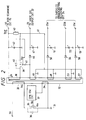
- FIG. 1 is a block diagram of the first embodiment of the power supply apparatus for the television receiver set and the television receiver set having the power supply apparatus.
- an ac power supply input terminal 1 receives an ac supply power and sends it to a remote control transformer through a main switch 2 and to a line filter 7 through the main switch 2 and a relay switch 4.
- the main switch 2 turns off all supply power of the television receiver set.
- the relay switch 4 is made close or open in response to a control signal 3 from a microprocessor 100.
- the remote control transformer 12 supplies an ac supply power with a desired voltage to a rectifying circuit 13 comprising a rectifying bridge 13 and a smooth capacitor 13b. An output of the rectifying circuit 13 is sent to the microprocessor 100.
- the line filter 7 supplies the ac supply power with noise components removed to a rectifying circuit 27 comprising a rectifying bridge 27a and a smoothing capacitor 27b of electrolytic capacitor wherein diodes of the rectifying bridge and the capacitor have larger capacitances than those of the prior art shown in Fig. 9 respectively.
- An output of the rectifying circuit 27 is sent to a regenerative type of switching power supply 26.
- the switching power supply 26 generates and sends a dc supply voltage 17 to a horizontal scanning circuit 21 through a relay switch 29, a set of dc supply voltages 25 to a satellite broadcasting receiving circuit 24 directly, and a supply voltage 23 to a voice signal output circuit 22 also directly.
- the set of the dc supply voltages include a first supply voltage 25a of 18 volts, a second supply voltage 25b of 12 volts, and a third supply voltage 25c of 9 volts.
- the microprocessor 100 produces a control signal 28 which is applied to the relay switch 29 for causing the television receiver set to enter the automatic recording condition. That is, the relay switch 29 is turned on/off by the control signal 28 from the microprocessor 100 and is provided between the switching power supply 26 and the horizontal scanning circuit 15.
- the horizontal scanning circuit 16 generates flyback pulses 16 which is sent to a high voltage generation circuit 14.
- the high voltage generation circuit 14 produces a high voltage supply voltage 19 which is sent to a vertical scanning circuit 18 and another high voltage supply voltage 21 is sent to a video signal processing circuit 20.
- the supply voltages are produced as follows: The ac voltage from the ac input terminal 1 is passed through a line filter 7 and is rectified by the rectifying circuit 27.
- the switching power supply 26 starts oscillation and outputs voltages at its secondary circuit. Then, the switching power supply 26 supplies the supply voltage 17, the supply voltage 23, and the set of supply voltages 25 to the horizontal scanning circuit 15, the voice signal output circuit 22, and the satellite broadcasting receiving circuit 24 respectively as shown in Fig. 1.
- all circuits in the television for displaying image pictures and outputting voice sounds operate, so that the television receiver set is in a condition that the user can watch programs of the ordinal television broadcasting and the satellite broadcasting at will.
- an automatic recording mode for recording a program of the satellite broadcasting automatically will be descried.
- the meaning of the automatic recording mode is the same as that of the prior art mentioned above, so that detailed description is omitted.
- the microprocessor 100 When the user sends to the television receiver set a command for automatic recording by a remote controller (not shown) or by a keyboard (not shown) on the front of the television receiver set, in response to the command, the microprocessor 100 outputs the control signal 28 so as to open the relay switch 29. Then, the switching power supply 26 continues operation and output of each of supply powers. However, the supply voltage 17 is not supplied to the horizontal scanning circuit 15, so that the flyback pulse 16 is not generated and the high voltage generation circuit 14 stops operation. This causes that the supply voltages 19 and 21 are not supplied to the vertical scanning circuit 18 and the video signal processing circuit 20 from the secondary circuit of the flyback transformer to the high voltage generation circuit 14 respectively. This condition is the same as the condition that the prior art switching power supply 10 is not in operation shown in Fig. 9 because all circuits for display, that is, television circuit portion, are not in operation. Therefore, this establishes the automatic recording condition that only the satellite broadcasting receiving circuit 24 is supplied with the supply voltage 25.
- Fig. 2 is a schematic circuit diagram of the switching power supply 26 used in all embodiments of this invention.
- An input terminal 30 receives the supply voltage from the rectifying circuit 27 shown in Fig. 1.
- a primary current I D flows from the input terminal 30 to an earth terminal 31 through a primary winding 33 and a switching element 35 using a field effect transistor (hereinafter referred to as FET).
- FET field effect transistor
- the primary circuit of the switching power supply comprises the primary winding 33 of a transformer 32 and the switching element 35 connected in series with the primary winding 33, a body diode 36 parasitically included in the switching element 35 and the bias winding 34 whose one end is connected to a synchronous oscillating circuit 37 and another end is connected to the earth terminal 31.
- the body diode 36 included in the switching element is used for regenerating energy stored in the transformer 32 through the above-mentioned primary winding 33. That is, it is used to flow a regeneration current in the primary winding 33 when the switching element 35 is turned off.
- the synchronous oscillation circuit 37 for maintaining oscillation by repeating turning on and off such as to turn on the switching element 35 for a predetermined ON period and then, to maintain turning off until a polarity of the induced voltage of the above-mentioned bias winding 34 is inverted.
- the secondary winding 38 of the transformer 32 generates the power supply voltage 44 for the horizontal scanning circuit 15, whose one end is for outputting the supply voltage 44 and another end is connected to a switching element 39 using an FET in series.
- a body diode 40 is a parasitically produced which is associated with the switching element 39 and is connected in parallel with the switching element 39.
- a gate of the FET 39 is connected to a control circuit 43 and to the supply voltage 48 through a drive resistor 41 for the switching element 39.
- the transformer 32 comprises a secondary windings 45, 49, 53, and 57.
- On end of the winding 45 is connected to a rectifying diode 46 in series.
- the output of the diode 46 is connected to a smoothing capacitor 47 in parallel.
- the secondary winding 49, 53, and 57 are provided for supply voltages 52, 56, and 60 respectively, which are supplied to the satellite broadcasting receiver 24.
- Fig. 3 shows waveforms of the regenerative type of power supply of the invention.
- an waveform 102 is of a voltage VDS between both ends of the switching element 35;
- an waveform 103 is of a primary current ID flowing through the above-mentioned primary winding 33;
- an waveform 104 is of a drive pulse VG1 of the synchronous oscillating circuit 37;
- an waveform 105 is of a secondary current waveform Io flowing though the above-mentioned secondary winding 38;
- an waveform 106 is of a drive pulse VG2 of the switching element 39 of the secondary circuit wherein periods denoted by slant lines out of OFF periods show the counter current periods for flowing a secondary current in the above-mentioned secondary winding 38.
- a primary current flowing through the primary winding 33 for an ON period of the switching element 35 which operates for the ON period determined by the synchronous oscillating circuit 37 generates a magnetic flux in the transformer 32 and thus, energy is accumulated.
- an induced voltage is developed in the secondary winding 38 of the transformer 32.
- the secondary circuit is so formed that the body diode 40 is reverse-biased and the switching element 39 of the secondary circuit turns off.
- a flyback voltage is generated in the above-mentioned primary winding 33 as well as a flyback voltage is also developed in the winding 38 so as to apply to the body diode 40 in the form of forward-bias.
- the energy accumulated in the transformer 32 is released as a secondary current which is fed through the secondary winding 38 to the smoothing capacitor 42 which smooths it and provides the supply voltage 44.
- the switching element 39 of the secondary circuit is turned on by the flyback voltage developed in the secondary winding 45 which is applied thereto through the drive resistor 41.
- the secondary current flows through the body diode 40 or the switching element 39 as an FET.
- the smoothing capacitor produces a reverse current, so that an energy is accumulated in the transformer 32 with a magnetic flux having a direction opposite to the magnetic flux developed by the primary current ID flowing through the primary winding 33.
- a polarity of an induced voltage developed in each of windings of the transformer 32 does not change, so that the flyback voltage of the bias winding 34 also does not change.
- the synchronous oscillation circuit 37 maintains the OFF period of the switching element 35.
- the ON period of the switching element 39 of the secondary circuit is controlled by the control circuit 43.
- the switching element 39 of the secondary circuit turns off, the polarity of the induced voltage generated in each of windings of the transformer 32 is inverted, so that the induced voltage developed in the above-mentioned secondary winding 38 makes the body diode 40 biased in reverse. Moreover, the switching element 39 also turns off, so that the secondary winding current stops flowing. Then, the induced voltage developed in the above-mentioned primary winding 33 is so generated to cause a junction terminal of the switching element 35 to have a negative voltage and to make a junction terminal of the supply voltage 30 to have a positive voltage.
- a primary current flows in the direction such that it charges the supply voltage 30 through the body diode 36, so that energy accumulated in the transformer 32 for the OFF period is regenerated in the supply voltage 30.
- a polarity of the induced voltage in the bias winding 34 is also judged, so that the synchronous oscillation circuit 37 turns on the switching element 35.
- it does not effect on operational characteristic whichever the primary current flows through either one, manely, through the switching element 35 or body diode 36.
- secondary windings 45, 49, 53, and 57 of multi-output type windings are provided for a multi-output structure in this embodiment.
- a flyback voltage is generated in the secondary winding 45 when the switching element 35 turns off, it is applied to the rectifying diode 46 with forward biasing, so that a current flows through the rectifying diode 46 by energy stored in the transformer 32 and is smoothed by the smoothing capacitor 47 to output it.
- Operations at this instance in other secondary windings 49, 53,and 57 are the same as each other, so that a description is omitted.
- Fig. 3 shows each of waveforms of output voltage in operation. It is assumed that the OFF period (t1-t3) of the drive pulse VG1 generated by the synchronous oscillation circuit 37 is TOFF; in this period, the counter current period (t2-t3) of the secondary current I o is T'OFF; an ON period (t3-t5) is TON; in this period, a regeneration period (t3-t4) of the primary current ID is T'ON.
- the TOFF is constant and the oscillation frequency f is also constant if the output voltage, the output voltage 44, for example, is constant because the ON period TON is retained to be a constant value determined by the synchronous oscillation circuit 37.
- the counter current period T'OFF can be changed by the switching element 39 of the secondary circuit, which is controlled by the control circuit 43.
- the output voltage can be controlled by changing the current period T'OFF when the output current Iout changes.
- the supply voltage 44 as the output voltage Vout is controlled to be continuously constant by changing the counter current period T'OFF.
- the control circuit 43 controls the ON period of the switching element 39 of the secondary circuit to determine the counter current period T'OFF.
- Fig. 4 shows each of operational waveforms of the regenerative type of the switching power supply 11 when the output current Iout changes. Some waveforms out of the waveforms shown in Fig. 4 are the same as those of Fig. 3 and thus, description about such waveforms are omitted.
- solid lines show the output current Iout flows with the maximum value, i.e., that of maximum load. Chain lines shows the case of that the output current is zero, i.e., unloaded condition.
- Fig. 5 shows an output voltage characteristic of the regenerative type of the switching power supply of the invention with respect to change of a load.
- the axis of ordinate is the secondary output voltage and respective values correspond supply voltages 48, 52, 56, and 60.
- the axis of abscissas shows a total of load electric power taken from the secondary circuit. As shown in Fig. 5, the output voltage is constant over a rang from no load to the maximum load.
- Fig. 6 is a block diagram of a second embodiment of the television receiver set having the power supply apparatus.
- the structure of the second embodiment is the same as that of the first embodiment basically.
- a character broadcasting receiving circuit 64 and a switch circuit 63 are added to the structure shown in Fig. 1.
- the switch circuit 63 is controlled by a control signal 62 from the microprocessor 100 and is provided between the character display broadcasting receiving circuit 64 and the supply voltage 64 from the supply voltage 25.
- the supply voltage 64 is obtained by branching off the supply voltages 25a and 25b.
- Operation of the automatic recording of the satellite broadcasting is performed as similar to the structure of Fig. 1 basically.
- the user gives the microprocessor 100 a command for selecting whether the supply voltage 64 is supplied to the character display broadcasting receiving circuit 65 by turning on or off the switch circuit 63.
- This causes stop of the circuits 14, 15 18, 20, and 22 for displaying in the absence of the user and operation of only the character broadcasting receiving circuit 65 which stores the content of a given character broadcasting in its memory (not shown).
- the user can watch it by reproducing with the memory at a desired time.
- the user can effect automatic recording of the above-mentioned satellite broadcasting and character broadcasting by selection from either the condition that only the satellite broadcasting receiving circuit 24 operates or the condition that both the satellite broadcasting receiving circuit 24 and the character broadcasting receiving circuit 65 are in operating. That is, in this structure, it is impossible to operate only the character broadcasting receiving circuit 65.
- Fig. 7 is a block diagram of the third embodiment of the power supply apparatus for the television receiver set and the television receiver set having the power supply apparatus.
- the structure of the third embodiment is the same as that of the first embodiment basically. There are differences that a switch circuit 67 are added to the structure shown in Fig. 1 and the remote transformer 12 and rectifying circuit 13 are replaced with a three-terminal regulator (dc-dc converter) 70.
- the switch circuit 67 is provided between the switching power supply 26 and the satellite broadcasting receiving circuit 24.
- the three-terminal regulator 70 is connected to the supply voltage 25a which is one of supply voltages of the switching regulator 26.
- the three-terminal regulator 70 generates a supply voltage 71 for the microprocessor 100 as a standby supply voltage.
- the switching power supply 26 supplies the supply voltage 17, the supply voltage 23, and the supply voltage 25 to the horizontal scanning circuit 15, the voice signal output circuit 22, and the satellite broadcasting receiving circuit 24 respectively as shown in Fig. 7.
- the switching power supply 26 supplies the supply voltage 17, the supply voltage 23, and the supply voltage 25 to the horizontal scanning circuit 15, the voice signal output circuit 22, and the satellite broadcasting receiving circuit 24 respectively as shown in Fig. 7.
- the standby condition is that only the microprocessor 100 operates as a load of the power supply 26. In this condition the user can selects watching of the television with the remote controller (not shown).
- the microprocessor 100 When the user sends to the television a command for automatic recording with the remote controller (not shown) or by a keyboard (not shown) on the front of the television receiver set, in response to the command, the microprocessor 100 outputs the control signals 28 and 66 so as to open the switches 29 and 67. If the standby condition is started from the condition that automatic recording has carried out, the microprocessor 100 outputs only the control signal 66 to turn off the satellite broadcasting receiving circuit 24. Then, the switching power supply 26 continues operation and output of each of supply powers. However, the supply voltage 17 is not supplied to the horizontal scanning circuit 15, so that the flyback pulse 16 is not generated and the high voltage generation circuit 14 stops operation.
- the switching power supply 26 supplies only supply power 71 to the microprocessor 100 through the three-terminal regulator 70. This establishes the standby condition.
- Fig. 8 is a block diagram of the fourth embodiment of the power supply apparatus for the television receiver set and the television receiver set having the power supply apparatus.
- the structure of the fourth embodiment is the same as that of the third embodiment basically. There are differences that a character broadcasting receiving circuit 65 and a switch circuit 63 are added to the structure shown in Fig. 8.
- the switch circuit 63 is controlled by a control signal 62 from the microprocessor 100 and is provided between the character display broadcasting receiving circuit 64 and the supply voltage 64 from the supply voltage 25.
- the supply voltage 64 is obtained branching off the supply voltages 25a and 25b.
- Operation of the automatic recording of the satellite broadcasting is established as similar to the structure of Fig. 7.
- the user gives the microprocessor a command for selecting whether the supply voltage 64 is supplied to the character display broadcasting receiving circuit 71 on or not by turning on or off the switch circuit 65.
- This causes stop of the circuit for displaying during the absence of the user and causes operation of the character broadcasting receiving circuit 65 by storing the content of a given character broadcasting program in the memory (not shown) of the character broadcasting receiving circuit 65.
- the user can watch it at a desired time.
- description about transition to the standby condition is omitted because it is the same as that of the third embodiment of Fig. 7.
- the user can effect automatic recording of the above-mentioned satellite broadcasting and character broadcasting with selection from either the condition that only the satellite broadcasting receiving circuit 24 operates or the condition that both the satellite broadcasting receiving circuit 24 and the character broadcasting receiving circuit 65 are in operating.
- it is impossible to operate only the character broadcasting receiving circuit 65.
- only the character broadcasting receiving circuit 65 operates, if the circuit positions of the satellite broadcasting receiving circuit 24 and the character broadcasting receiving circuit 65 in the block diagram of Fig. 8 are replaced with each other.
- both of the satellite broadcasting receiving circuit 24 and character broadcasting receiving circuit 65 can be operated if two power supply systems are provided to the switching power supply 26 and connected to the satellite broad casting receiving circuit 24 and the character broadcasting receiving circuit 65 respectively.
- the microprocessor 100 is supplied with a standby supply through the three-terminal regulator 70. However, if one of supply voltages matches to the microprocessor 100 in voltage intensity, it can be supplied to the microprocessor 100 directly.
- controlling of supplying of supply voltages 17, 23, 25, 64, and 68 is carried out under control of the microprocessor.
- the power supply apparatus is realized with only one system contrary to the prior art switching power supply apparatus, so that there are provided advantageous effects that the mounting area for the power supply apparatus can be reduced to about half and reduce its cost.
- a power supply apparatus for the television receiver set comprising a television receiving circuit and other receiving circuits, for example, satellite broadcasting receiving circuit or character broadcasting receiving circuit, each of receiving circuit is supplied with a supply power from the same switching power supply of regenerative type having plural secondary windings wherein some receivers are selectively turned off by switches provided the receivers and the switching power supply for automatic recording or standby mode.
- the regenerative type of switching power supply has a stable output characteristic over a range from no load to the maximum load because of regenerative operation.
- the horizontal scanning circuit is turned off by the switch. This causes the horizontal scanning circuit and vertical scanning and video signal processing circuits to stop operation because supply power of the vertical scanning and video processing circuits are supplied with power from the horizontal scanning circuit through a high voltage generation circuit.
- the television having satellite broadcasting circuit and such power supply apparatus is also disclosed.
Landscapes
- Engineering & Computer Science (AREA)
- Multimedia (AREA)
- Signal Processing (AREA)
- Television Receiver Circuits (AREA)
Applications Claiming Priority (4)
| Application Number | Priority Date | Filing Date | Title |
|---|---|---|---|
| JP258001/90 | 1990-09-26 | ||
| JP2258001A JP2858370B2 (ja) | 1990-09-26 | 1990-09-26 | テレビジョン用電源装置 |
| JP300801/90 | 1990-11-05 | ||
| JP2300801A JPH04172090A (ja) | 1990-11-05 | 1990-11-05 | テレビジョン用電源装置 |
Publications (3)
| Publication Number | Publication Date |
|---|---|
| EP0477891A2 true EP0477891A2 (fr) | 1992-04-01 |
| EP0477891A3 EP0477891A3 (en) | 1992-06-10 |
| EP0477891B1 EP0477891B1 (fr) | 1996-07-10 |
Family
ID=26543490
Family Applications (1)
| Application Number | Title | Priority Date | Filing Date |
|---|---|---|---|
| EP91116310A Revoked EP0477891B1 (fr) | 1990-09-26 | 1991-09-25 | Appareil d'alimentation de puissance pour récepteur de télévision et récepteur de télévision avec un tel appareil |
Country Status (3)
| Country | Link |
|---|---|
| US (1) | US5331354A (fr) |
| EP (1) | EP0477891B1 (fr) |
| DE (1) | DE69120756T2 (fr) |
Cited By (5)
| Publication number | Priority date | Publication date | Assignee | Title |
|---|---|---|---|---|
| GB2257879A (en) * | 1991-07-19 | 1993-01-20 | Matsushita Electric Industrial Co Ltd | Power supply for television with built-in satellite tuner |
| EP0536553A1 (fr) * | 1991-09-10 | 1993-04-14 | Sony Corporation | Récepteurs de télévision |
| EP0776128A3 (fr) * | 1995-10-27 | 1998-07-08 | NOKIA TECHNOLOGY GmbH | Dispositifs vidéo télécommandés |
| EP0866609A1 (fr) * | 1993-01-30 | 1998-09-23 | Deutsche Thomson-Brandt Gmbh | Enregistreur vidéo |
| EP1458185A1 (fr) * | 2003-03-14 | 2004-09-15 | ORION ELECTRIC CO., Ltd. | Contrôleur d'alimentation pour équipement électronique combiné |
Families Citing this family (26)
| Publication number | Priority date | Publication date | Assignee | Title |
|---|---|---|---|---|
| GB9008898D0 (en) * | 1990-04-20 | 1990-06-20 | Ferguson Ltd | Receiver for satellite reception |
| JP3252378B2 (ja) * | 1992-03-30 | 2002-02-04 | ソニー株式会社 | 衛星放送受信装置 |
| JP3361909B2 (ja) * | 1995-03-03 | 2003-01-07 | エヌイーシー三菱電機ビジュアルシステムズ株式会社 | ディスプレイ装置 |
| US5940147A (en) * | 1995-06-01 | 1999-08-17 | U.S. Philips Corporation | Power supply synchronization |
| US6759759B2 (en) * | 2000-08-29 | 2004-07-06 | Tamagawa Seiki Kabushiki Kaisha | Rotary contactless connector and non-rotary contactless connector |
| US8098582B2 (en) * | 2005-03-31 | 2012-01-17 | At&T Intellectual Property I, L.P. | Methods, systems, and computer program products for implementing bandwidth control services |
| US8335239B2 (en) * | 2005-03-31 | 2012-12-18 | At&T Intellectual Property I, L.P. | Methods, systems, and devices for bandwidth conservation |
| US8024438B2 (en) * | 2005-03-31 | 2011-09-20 | At&T Intellectual Property, I, L.P. | Methods, systems, and computer program products for implementing bandwidth management services |
| US8306033B2 (en) * | 2005-03-31 | 2012-11-06 | At&T Intellectual Property I, L.P. | Methods, systems, and computer program products for providing traffic control services |
| US7975283B2 (en) * | 2005-03-31 | 2011-07-05 | At&T Intellectual Property I, L.P. | Presence detection in a bandwidth management system |
| US9432710B2 (en) * | 2005-07-08 | 2016-08-30 | At&T Intellectual Property I, L.P. | Methods systems, and products for conserving bandwidth |
| US8225410B2 (en) | 2005-07-08 | 2012-07-17 | At&T Intellectual Property I, L. P. | Methods, systems, and devices for securing content |
| US8701148B2 (en) | 2005-09-01 | 2014-04-15 | At&T Intellectual Property I, L.P. | Methods, systems, and devices for bandwidth conservation |
| US8104054B2 (en) * | 2005-09-01 | 2012-01-24 | At&T Intellectual Property I, L.P. | Methods, systems, and devices for bandwidth conservation |
| US20070253675A1 (en) * | 2006-04-28 | 2007-11-01 | Weaver Timothy H | Methods, systems, and products for recording media |
| US7647464B2 (en) | 2006-04-28 | 2010-01-12 | At&T Intellectual Property, I,L.P. | Methods, systems, and products for recording media to a restoration server |
| US20070255913A1 (en) * | 2006-04-28 | 2007-11-01 | Timothy Weaver | Methods, systems, and products for recording media |
| US8245267B2 (en) | 2006-04-28 | 2012-08-14 | At&T Intellectual Property I, L.P. | Methods, systems, and products for recording media on a user device |
| US7650368B2 (en) * | 2007-02-07 | 2010-01-19 | At&T Intellectual Property I, L.P. | Methods, systems, and products for restoring electronic media |
| US7711733B2 (en) * | 2007-02-07 | 2010-05-04 | At&T Intellectual Property I,L.P. | Methods, systems, and products for targeting media for storage to communications devices |
| US8379012B2 (en) * | 2009-07-17 | 2013-02-19 | Atmel Corporation | Selector switch for direct connection of switched regulator to voltage inputs |
| JP5271415B2 (ja) * | 2009-08-10 | 2013-08-21 | 株式会社東芝 | 電子機器および電子システム |
| US8476875B2 (en) | 2010-10-12 | 2013-07-02 | Allegro Microsystems, LLC. | TV set top box with an improved ability to survive a transient signal |
| JP2012222991A (ja) * | 2011-04-11 | 2012-11-12 | Funai Electric Co Ltd | 電源回路 |
| JP5531005B2 (ja) * | 2011-12-26 | 2014-06-25 | 株式会社沖データ | 電子機器 |
| JP6335438B2 (ja) * | 2013-05-17 | 2018-05-30 | キヤノン株式会社 | スイッチ制御装置及び画像形成装置 |
Family Cites Families (16)
| Publication number | Priority date | Publication date | Assignee | Title |
|---|---|---|---|---|
| JPS58121876A (ja) * | 1982-01-14 | 1983-07-20 | Matsushita Electric Ind Co Ltd | テレビジヨン受像機 |
| FR2537744A1 (fr) * | 1982-12-10 | 1984-06-15 | Radiotechnique | Procede pour modifier dans des rapports differents diverses tensions d'une alimentation, et alimentation a decoupage a deux etats |
| US4731870A (en) * | 1984-11-23 | 1988-03-15 | The Johns Hopkins University | Platform transmitter terminal (PTT) for use with an ARGOS type satellite system and utilizing a solar array/rechargeable battery power source |
| AU591095B2 (en) * | 1985-02-18 | 1989-11-30 | Plessey Overseas Limited | Improvements in or relating to radio transmitters |
| JPS628674A (ja) * | 1985-07-05 | 1987-01-16 | Matsushita Electric Ind Co Ltd | 電源装置 |
| US4751580A (en) * | 1985-12-19 | 1988-06-14 | Rca Licensing Corporation | Television receiver standby power supply |
| KR910006374B1 (ko) * | 1986-08-22 | 1991-08-21 | 삼성전자 주식회사 | 영상처리 시스템의 전원공급 및 입력신호 조절회로 |
| DE3723892A1 (de) * | 1987-07-18 | 1989-01-26 | Thomson Brandt Gmbh | Fernsehgeraet mit integrierter satelliten-empfangseinheit |
| DE3731645A1 (de) * | 1987-09-19 | 1989-03-30 | Thomson Brandt Gmbh | Schaltnetzteil |
| JP2811670B2 (ja) * | 1988-01-12 | 1998-10-15 | ソニー株式会社 | 受信機 |
| JPH01245772A (ja) * | 1988-03-28 | 1989-09-29 | Seiko Epson Corp | 文字多重放送受信機能付きカラーテレビ |
| US4945465A (en) * | 1988-09-15 | 1990-07-31 | U.S. Philips Corporation | Switched-mode power supply circuit |
| JPH02302184A (ja) * | 1989-05-16 | 1990-12-14 | Mitsubishi Electric Corp | 衛星放送受信機 |
| US5036261A (en) * | 1989-08-11 | 1991-07-30 | Thomson Consumer Electronics, Inc. | Standby/run power supply and control circuit |
| JP2979596B2 (ja) * | 1990-07-27 | 1999-11-15 | ソニー株式会社 | 表示装置 |
| US5168436A (en) * | 1990-09-26 | 1992-12-01 | Allied-Signal Inc. | Uninterruptible power supply |
-
1991
- 1991-09-25 US US07/765,345 patent/US5331354A/en not_active Expired - Fee Related
- 1991-09-25 DE DE69120756T patent/DE69120756T2/de not_active Expired - Fee Related
- 1991-09-25 EP EP91116310A patent/EP0477891B1/fr not_active Revoked
Cited By (9)
| Publication number | Priority date | Publication date | Assignee | Title |
|---|---|---|---|---|
| GB2257879A (en) * | 1991-07-19 | 1993-01-20 | Matsushita Electric Industrial Co Ltd | Power supply for television with built-in satellite tuner |
| US5341179A (en) * | 1991-07-19 | 1994-08-23 | Matsushita Electric Industrial Co., Ltd. | Source voltage control switching circuit |
| GB2257879B (en) * | 1991-07-19 | 1995-05-03 | Matsushita Electric Industrial Co Ltd | Source voltage control switching circuit |
| EP0536553A1 (fr) * | 1991-09-10 | 1993-04-14 | Sony Corporation | Récepteurs de télévision |
| US5313282A (en) * | 1991-09-10 | 1994-05-17 | Sony Corporation | Device for controlling power supplied to a satellite broadcast receiver in a television |
| EP0866609A1 (fr) * | 1993-01-30 | 1998-09-23 | Deutsche Thomson-Brandt Gmbh | Enregistreur vidéo |
| CN1085468C (zh) * | 1993-01-30 | 2002-05-22 | 德国汤姆森-勃朗特有限公司 | 用户电子装置用的供电回路 |
| EP0776128A3 (fr) * | 1995-10-27 | 1998-07-08 | NOKIA TECHNOLOGY GmbH | Dispositifs vidéo télécommandés |
| EP1458185A1 (fr) * | 2003-03-14 | 2004-09-15 | ORION ELECTRIC CO., Ltd. | Contrôleur d'alimentation pour équipement électronique combiné |
Also Published As
| Publication number | Publication date |
|---|---|
| EP0477891B1 (fr) | 1996-07-10 |
| US5331354A (en) | 1994-07-19 |
| EP0477891A3 (en) | 1992-06-10 |
| DE69120756D1 (de) | 1996-08-14 |
| DE69120756T2 (de) | 1996-12-05 |
Similar Documents
| Publication | Publication Date | Title |
|---|---|---|
| EP0477891B1 (fr) | Appareil d'alimentation de puissance pour récepteur de télévision et récepteur de télévision avec un tel appareil | |
| US4941078A (en) | Synchronized switch-mode power supply | |
| JPH0227870B2 (fr) | ||
| US5949660A (en) | Switched-mode power supply having a standby mode | |
| EP0720363B1 (fr) | Répartition de consommation minimum en attente | |
| CA2073700C (fr) | Circuit de commutation de la tension de source | |
| CA2072321C (fr) | Recepteur de television sans luminosite remanente a ecran protege contre les brulures | |
| KR920002841B1 (ko) | 텔레비젼 수상기용 스위칭모드 파워 서플라이 | |
| CA1279925C (fr) | Regulateur d'alimentation pour television | |
| US4968106A (en) | High voltage generating apparatus for television equipment | |
| US4392090A (en) | Remote responsive television receiver ferroresonant power supply | |
| US6157549A (en) | Power supply with multiple mode operation | |
| JP2858370B2 (ja) | テレビジョン用電源装置 | |
| US4190791A (en) | Switching regulator for television deflection circuit with improved ultor voltage regulation | |
| US5142206A (en) | Slow turn-on in a deflection circuit | |
| KR960007921B1 (ko) | 멀티모드 모니터의 전원전압 제어회로 | |
| GB2230114A (en) | A switch-mode power supply | |
| US3970779A (en) | Power supply circuit | |
| EP0996285B1 (fr) | Alimentation à modes multiples de fonctionnement | |
| US4000441A (en) | Horizontal deflection circuit for television receivers having an auxiliary power supply | |
| JPH04172090A (ja) | テレビジョン用電源装置 | |
| JPH06125514A (ja) | 誤差増幅装置 | |
| US4298830A (en) | Horizontal deflection generator and driver circuit | |
| JPH05176258A (ja) | テレビジョン用電源装置 | |
| KR950010736B1 (ko) | 텔레비젼 수상기의 화면비 변환장치 |
Legal Events
| Date | Code | Title | Description |
|---|---|---|---|
| PUAI | Public reference made under article 153(3) epc to a published international application that has entered the european phase |
Free format text: ORIGINAL CODE: 0009012 |
|
| 17P | Request for examination filed |
Effective date: 19911024 |
|
| AK | Designated contracting states |
Kind code of ref document: A2 Designated state(s): DE FR GB |
|
| PUAL | Search report despatched |
Free format text: ORIGINAL CODE: 0009013 |
|
| AK | Designated contracting states |
Kind code of ref document: A3 Designated state(s): DE FR GB |
|
| 17Q | First examination report despatched |
Effective date: 19940510 |
|
| GRAH | Despatch of communication of intention to grant a patent |
Free format text: ORIGINAL CODE: EPIDOS IGRA |
|
| GRAH | Despatch of communication of intention to grant a patent |
Free format text: ORIGINAL CODE: EPIDOS IGRA |
|
| GRAH | Despatch of communication of intention to grant a patent |
Free format text: ORIGINAL CODE: EPIDOS IGRA |
|
| GRAA | (expected) grant |
Free format text: ORIGINAL CODE: 0009210 |
|
| AK | Designated contracting states |
Kind code of ref document: B1 Designated state(s): DE FR GB |
|
| GRAH | Despatch of communication of intention to grant a patent |
Free format text: ORIGINAL CODE: EPIDOS IGRA |
|
| REF | Corresponds to: |
Ref document number: 69120756 Country of ref document: DE Date of ref document: 19960814 |
|
| ET | Fr: translation filed | ||
| PLBQ | Unpublished change to opponent data |
Free format text: ORIGINAL CODE: EPIDOS OPPO |
|
| PLBI | Opposition filed |
Free format text: ORIGINAL CODE: 0009260 |
|
| PLBF | Reply of patent proprietor to notice(s) of opposition |
Free format text: ORIGINAL CODE: EPIDOS OBSO |
|
| 26 | Opposition filed |
Opponent name: INTERESSENGEMEINSCHAFT FUER RUNDFUNKSCHUTZRECHTE G Effective date: 19970410 |
|
| PLBF | Reply of patent proprietor to notice(s) of opposition |
Free format text: ORIGINAL CODE: EPIDOS OBSO |
|
| PLBF | Reply of patent proprietor to notice(s) of opposition |
Free format text: ORIGINAL CODE: EPIDOS OBSO |
|
| PLBO | Opposition rejected |
Free format text: ORIGINAL CODE: EPIDOS REJO |
|
| PLBN | Opposition rejected |
Free format text: ORIGINAL CODE: 0009273 |
|
| APAC | Appeal dossier modified |
Free format text: ORIGINAL CODE: EPIDOS NOAPO |
|
| PLAE | Information related to rejection of opposition modified |
Free format text: ORIGINAL CODE: 0009299REJO |
|
| APAE | Appeal reference modified |
Free format text: ORIGINAL CODE: EPIDOS REFNO |
|
| 27O | Opposition rejected |
Effective date: 19991012 |
|
| APAC | Appeal dossier modified |
Free format text: ORIGINAL CODE: EPIDOS NOAPO |
|
| D27O | Information related to the rejection of opposition deleted | ||
| REG | Reference to a national code |
Ref country code: GB Ref legal event code: IF02 |
|
| APBY | Invitation to file observations in appeal sent |
Free format text: ORIGINAL CODE: EPIDOSNOBA2O |
|
| APBY | Invitation to file observations in appeal sent |
Free format text: ORIGINAL CODE: EPIDOSNOBA2O |
|
| APCA | Receipt of observations in appeal recorded |
Free format text: ORIGINAL CODE: EPIDOSNOBA4O |
|
| PGFP | Annual fee paid to national office [announced via postgrant information from national office to epo] |
Ref country code: FR Payment date: 20050823 Year of fee payment: 15 |
|
| PGFP | Annual fee paid to national office [announced via postgrant information from national office to epo] |
Ref country code: GB Payment date: 20050921 Year of fee payment: 15 |
|
| PGFP | Annual fee paid to national office [announced via postgrant information from national office to epo] |
Ref country code: DE Payment date: 20050922 Year of fee payment: 15 |
|
| APAH | Appeal reference modified |
Free format text: ORIGINAL CODE: EPIDOSCREFNO |
|
| APBU | Appeal procedure closed |
Free format text: ORIGINAL CODE: EPIDOSNNOA9O |
|
| RDAF | Communication despatched that patent is revoked |
Free format text: ORIGINAL CODE: EPIDOSNREV1 |
|
| RDAG | Patent revoked |
Free format text: ORIGINAL CODE: 0009271 |
|
| STAA | Information on the status of an ep patent application or granted ep patent |
Free format text: STATUS: PATENT REVOKED |
|
| 27W | Patent revoked |
Effective date: 20050316 |
|
| GBPR | Gb: patent revoked under art. 102 of the ep convention designating the uk as contracting state |
Free format text: 20050316 |