EP0477907B1 - Circuit de courant constant et un circuit oscillant commandé par ledit circuit - Google Patents
Circuit de courant constant et un circuit oscillant commandé par ledit circuit Download PDFInfo
- Publication number
- EP0477907B1 EP0477907B1 EP91116347A EP91116347A EP0477907B1 EP 0477907 B1 EP0477907 B1 EP 0477907B1 EP 91116347 A EP91116347 A EP 91116347A EP 91116347 A EP91116347 A EP 91116347A EP 0477907 B1 EP0477907 B1 EP 0477907B1
- Authority
- EP
- European Patent Office
- Prior art keywords
- constant current
- circuit
- voltage
- transistors
- transistor
- Prior art date
- Legal status (The legal status is an assumption and is not a legal conclusion. Google has not performed a legal analysis and makes no representation as to the accuracy of the status listed.)
- Expired - Lifetime
Links
Images





Classifications
-
- H—ELECTRICITY
- H03—ELECTRONIC CIRCUITRY
- H03B—GENERATION OF OSCILLATIONS, DIRECTLY OR BY FREQUENCY-CHANGING, BY CIRCUITS EMPLOYING ACTIVE ELEMENTS WHICH OPERATE IN A NON-SWITCHING MANNER; GENERATION OF NOISE BY SUCH CIRCUITS
- H03B5/00—Generation of oscillations using amplifier with regenerative feedback from output to input
-
- G—PHYSICS
- G05—CONTROLLING; REGULATING
- G05F—SYSTEMS FOR REGULATING ELECTRIC OR MAGNETIC VARIABLES
- G05F3/00—Non-retroactive systems for regulating electric variables by using an uncontrolled element, or an uncontrolled combination of elements, such element or such combination having self-regulating properties
- G05F3/02—Regulating voltage or current
- G05F3/08—Regulating voltage or current wherein the variable is DC
- G05F3/10—Regulating voltage or current wherein the variable is DC using uncontrolled devices with non-linear characteristics
- G05F3/16—Regulating voltage or current wherein the variable is DC using uncontrolled devices with non-linear characteristics being semiconductor devices
- G05F3/20—Regulating voltage or current wherein the variable is DC using uncontrolled devices with non-linear characteristics being semiconductor devices using diode- transistor combinations
- G05F3/26—Current mirrors
- G05F3/265—Current mirrors using bipolar transistors only
-
- G—PHYSICS
- G05—CONTROLLING; REGULATING
- G05F—SYSTEMS FOR REGULATING ELECTRIC OR MAGNETIC VARIABLES
- G05F3/00—Non-retroactive systems for regulating electric variables by using an uncontrolled element, or an uncontrolled combination of elements, such element or such combination having self-regulating properties
- G05F3/02—Regulating voltage or current
- G05F3/08—Regulating voltage or current wherein the variable is DC
- G05F3/10—Regulating voltage or current wherein the variable is DC using uncontrolled devices with non-linear characteristics
- G05F3/16—Regulating voltage or current wherein the variable is DC using uncontrolled devices with non-linear characteristics being semiconductor devices
- G05F3/20—Regulating voltage or current wherein the variable is DC using uncontrolled devices with non-linear characteristics being semiconductor devices using diode- transistor combinations
- G05F3/22—Regulating voltage or current wherein the variable is DC using uncontrolled devices with non-linear characteristics being semiconductor devices using diode- transistor combinations wherein the transistors are of the bipolar type only
- G05F3/222—Regulating voltage or current wherein the variable is DC using uncontrolled devices with non-linear characteristics being semiconductor devices using diode- transistor combinations wherein the transistors are of the bipolar type only with compensation for device parameters, e.g. Early effect, gain, manufacturing process, or external variations, e.g. temperature, loading, supply voltage
- G05F3/227—Regulating voltage or current wherein the variable is DC using uncontrolled devices with non-linear characteristics being semiconductor devices using diode- transistor combinations wherein the transistors are of the bipolar type only with compensation for device parameters, e.g. Early effect, gain, manufacturing process, or external variations, e.g. temperature, loading, supply voltage producing a current or voltage as a predetermined function of the supply voltage
-
- H—ELECTRICITY
- H03—ELECTRONIC CIRCUITRY
- H03K—PULSE TECHNIQUE
- H03K3/00—Circuits for generating electric pulses; Monostable, bistable or multistable circuits
- H03K3/02—Generators characterised by the type of circuit or by the means used for producing pulses
- H03K3/023—Generators characterised by the type of circuit or by the means used for producing pulses by the use of differential amplifiers or comparators, with internal or external positive feedback
- H03K3/0231—Astable circuits
-
- H—ELECTRICITY
- H03—ELECTRONIC CIRCUITRY
- H03K—PULSE TECHNIQUE
- H03K4/00—Generating pulses having essentially a finite slope or stepped portions
- H03K4/06—Generating pulses having essentially a finite slope or stepped portions having triangular shape
- H03K4/08—Generating pulses having essentially a finite slope or stepped portions having triangular shape having sawtooth shape
- H03K4/48—Generating pulses having essentially a finite slope or stepped portions having triangular shape having sawtooth shape using as active elements semiconductor devices
- H03K4/50—Generating pulses having essentially a finite slope or stepped portions having triangular shape having sawtooth shape using as active elements semiconductor devices in which a sawtooth voltage is produced across a capacitor
- H03K4/501—Generating pulses having essentially a finite slope or stepped portions having triangular shape having sawtooth shape using as active elements semiconductor devices in which a sawtooth voltage is produced across a capacitor the starting point of the flyback period being determined by the amplitude of the voltage across the capacitor, e.g. by a comparator
- H03K4/502—Generating pulses having essentially a finite slope or stepped portions having triangular shape having sawtooth shape using as active elements semiconductor devices in which a sawtooth voltage is produced across a capacitor the starting point of the flyback period being determined by the amplitude of the voltage across the capacitor, e.g. by a comparator the capacitor being charged from a constant-current source
Definitions
- one of the following techniques is used for changing the clock signal frequency.
- the first is to provide multiple oscillators for generating clock signals of different frequencies, and to select a suitable one of the oscillators when performing, for example, a high-speed operation such as arithmetic processing or a low-speed operation such as mode selection.
- the second is to provide a single oscillator of a relatively high frequency, and obtain a desired low frequency by demultiplying the high frequency.
- both these techniques involve drawbacks of requiring extra hardware such as oscillators and selecting circuits, and of increase in the cost of the computers.
- Another drawback of the conventional techniques is that the clock frequency cannot be continuously varied.
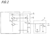
- the voltage detection circuit D1 detects the voltage V0 of the capacitor C0 and instructs the switch means SW to close on detecting V0 higher than a first predetermined voltage (V S1 ) and to open on detecting V0 lower than a second predetermined voltage (V S2 ).
- V S1 a first predetermined voltage
- V S2 a second predetermined voltage
- the capacitor C0 is subject to be charged or discharged along with the ON-OFF operation of the switch means SW, and V0 changes as a triangular wave of a constant frequency.
- the frequency can be varied by changing the power source voltage V cc as described later.
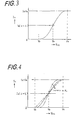
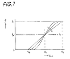
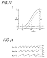
- FIG. 5 shows exemplary waveforms of the signal output from the oscillating circuit of Figure 2, corresponding to aforementioned specific V cc s of V3, V4 and V5, and Figure 6 shows the change in the frequency of the output signal with respect to the change of V cc .
- V S1 and V S2 represent the maximum and minimum of the voltages V0 at an end of the capacitor C0, respectively, which are detected by the voltage detection circuit D1 as described above with reference to Figure 2.
- V S1 is a voltage V0 where the discharging of the capacitor C0 initiates
- V S2 is a voltage V0 where the charging of the capacitor C0 initiates.
- the rise time of the output signal decreases as V cc increases, while the fall time of the signal is constant because it only depends on the resistance inherent in the switching means SW shown in Figure 2.
- V cc V3
- the frequency of the output signal is zero as shown in Figures 5 and 6, because the current I4 becomes zero and the capacitor C0 is not charged.
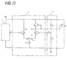
- the third embodiment of the present invention is shown in Figure 17, wherein the constant current circuit again has a configuration based on Figure 1 and is shown with an oscillating circuit of the Figure 2 type.
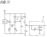
- Constant current supplying sources I C and I0 are provided, as explained above with reference to Figures 11 and 15.
- the transistors Q1 and Q2, both bipolar transistors, for example, and a resistor R1 constitute a source of reference voltage V1.
- the base-emitter junction voltage of the transistors Q1 and Q2 which are connected to each other in series and supplied with a bias current is used as a constant voltage source.
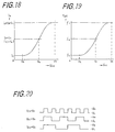
- the Schmitt circuit D2 has two threshold values of a high level S H and a low level S L , and jumps the output F OUT thereof to high level V H , if V O increases up to the high level threshold S H .
- the transistor Q9 turns on and the capacitor C0 is discharged. Accordingly, the voltage V0 decreases but the output remains at high level V H .
- the Schmitt circuit D2 jumps the output F OUT to low level V L .
- the transistor Q3 turns off and the capacitor C0 is stopped from discharging and begins charging by the current I4.
Landscapes
- Engineering & Computer Science (AREA)
- Microelectronics & Electronic Packaging (AREA)
- Physics & Mathematics (AREA)
- Power Engineering (AREA)
- Electromagnetism (AREA)
- General Physics & Mathematics (AREA)
- Radar, Positioning & Navigation (AREA)
- Automation & Control Theory (AREA)
- Nonlinear Science (AREA)
- Dc-Dc Converters (AREA)
- Inductance-Capacitance Distribution Constants And Capacitance-Resistance Oscillators (AREA)
- Electronic Switches (AREA)
- Control Of Electrical Variables (AREA)
- Continuous-Control Power Sources That Use Transistors (AREA)
- Amplifiers (AREA)
- Networks Using Active Elements (AREA)
Claims (3)
- Circuit à courant constant ayant une source pour fournir une tension d'alimentation (Vcc), des moyens fournissant un courant constant (IA, IB; ID) comprenant au moins une source fournissant un courant constant, des premier et deuxième transistors (Q3, Q5) montés entre la source fournissant une tension d'alimentation et les moyens fournissant un courant constant, chacun des transistors ayant une électrode de commande, et des moyens de résistance (R4), comprenant au moins une résistance, montés entre des noeuds respectifs des premier et deuxième transistors et connectés aux moyens fournissant un courant constant, caractérisé en ce que l'électrode de commande du premier transistor (Q3) reçoit une tension de référence (V1) et le circuti à courant constant comprend en outre un diviseur de tension (R2, R3) fournissant une tension divisée de la tension d'alimentation (Vcc) pour l'électrode de commande du deuxième transistor,
ce par quoi le courant circulant dans le deuxième transistor (Q5) est commandé selon l'amplitude de ladite tension d'alimentation, et la vitesse de variation du courant par rapport à la variation de la tension d'alimentation dépend de la résistance des moyens de résistance (R4), ladite résistance étant choisie de telle manière que le deuxième transistor (Q5) fournisse un courant qui varie linéairement avec la tension d'alimentation. - Circuit à courant constant selon la revendication 1, dans lequel les moyens fournissant un courant constant comprennent deux sources fournissant un courant constant (IA, IB), chacune connectée à un noeud respectif desdits noeuds des premier et deuxième transistors (Q3, Q5), et les moyens de résistance comprennent une seule résistance (R4) montée entre lesdits noeuds des premier et deuxième transistors et entre les deux sources fournissant un courant constant.
- Circuit à courant constant selon la revendication 1, dans leque les moyens fournissant un courant constant comprennent une seule source fournissant un courant constant (ID), et dans lequel les moyens de résistance (R4) comprennent des première et deuxième résistances (R41, R42) d'égale résistance montées en série entre lesdits noeuds des premier et deuxième transistors (Q3, Q5), la source unique fournissant un courant constant (ID) étant connectée à un noeud commun aux première et deuxième résistances (R41, R42).
Priority Applications (1)
| Application Number | Priority Date | Filing Date | Title |
|---|---|---|---|
| EP95102887A EP0664502A3 (fr) | 1990-09-26 | 1991-09-25 | Circuit oscillant. |
Applications Claiming Priority (2)
| Application Number | Priority Date | Filing Date | Title |
|---|---|---|---|
| JP2256294A JP2763393B2 (ja) | 1990-09-26 | 1990-09-26 | 定電流回路および発振回路 |
| JP256294/90 | 1990-09-26 |
Related Child Applications (1)
| Application Number | Title | Priority Date | Filing Date |
|---|---|---|---|
| EP95102887.7 Division-Into | 1991-09-25 |
Publications (3)
| Publication Number | Publication Date |
|---|---|
| EP0477907A2 EP0477907A2 (fr) | 1992-04-01 |
| EP0477907A3 EP0477907A3 (en) | 1993-06-30 |
| EP0477907B1 true EP0477907B1 (fr) | 1996-04-17 |
Family
ID=17290663
Family Applications (2)
| Application Number | Title | Priority Date | Filing Date |
|---|---|---|---|
| EP95102887A Ceased EP0664502A3 (fr) | 1990-09-26 | 1991-09-25 | Circuit oscillant. |
| EP91116347A Expired - Lifetime EP0477907B1 (fr) | 1990-09-26 | 1991-09-25 | Circuit de courant constant et un circuit oscillant commandé par ledit circuit |
Family Applications Before (1)
| Application Number | Title | Priority Date | Filing Date |
|---|---|---|---|
| EP95102887A Ceased EP0664502A3 (fr) | 1990-09-26 | 1991-09-25 | Circuit oscillant. |
Country Status (6)
| Country | Link |
|---|---|
| US (1) | US5146188A (fr) |
| EP (2) | EP0664502A3 (fr) |
| JP (1) | JP2763393B2 (fr) |
| KR (1) | KR950005155B1 (fr) |
| CA (1) | CA2052248C (fr) |
| DE (1) | DE69118798T2 (fr) |
Families Citing this family (9)
| Publication number | Priority date | Publication date | Assignee | Title |
|---|---|---|---|---|
| EP0689731A1 (fr) * | 1993-03-17 | 1996-01-03 | National Semiconductor Corporation | Circuit de glissemant de fréquence pour régulateur à découpage |
| US5349286A (en) * | 1993-06-18 | 1994-09-20 | Texas Instruments Incorporated | Compensation for low gain bipolar transistors in voltage and current reference circuits |
| US5619125A (en) * | 1995-07-31 | 1997-04-08 | Lucent Technologies Inc. | Voltage-to-current converter |
| US6441693B1 (en) * | 2001-03-20 | 2002-08-27 | Honeywell International Inc. | Circuit for voltage to linear duty cycle conversion |
| DE10121821B4 (de) * | 2001-05-04 | 2004-04-08 | Infineon Technologies Ag | Frequenzregelschaltung |
| DE10259384B3 (de) * | 2002-12-18 | 2004-05-13 | Siemens Ag | Vorrichtung zur Ermittlung des Energiezustandes eines Energiespeichers eines mobilen Datenträgers |
| JP5762755B2 (ja) * | 2010-01-18 | 2015-08-12 | ローム株式会社 | 発光素子の駆動回路およびそれを用いた発光装置 |
| JP6576306B2 (ja) | 2016-06-28 | 2019-09-18 | 三菱電機株式会社 | 電圧電流変換回路および負荷駆動回路 |
| CN109002076B (zh) * | 2017-06-07 | 2021-10-29 | 苏州瀚宸科技有限公司 | 电阻电流镜像电路、rssi电路及芯片 |
Citations (1)
| Publication number | Priority date | Publication date | Assignee | Title |
|---|---|---|---|---|
| EP0165748A1 (fr) * | 1984-06-11 | 1985-12-27 | Nec Corporation | Circuit oscillateur |
Family Cites Families (7)
| Publication number | Priority date | Publication date | Assignee | Title |
|---|---|---|---|---|
| US3870971A (en) * | 1973-03-17 | 1975-03-11 | Victor Company Of Japan | Circuit arrangement of voltage controlled oscillator |
| US3831113A (en) * | 1973-06-01 | 1974-08-20 | Rca Corp | Relaxation oscillator |
| DE2912492A1 (de) * | 1979-03-29 | 1980-10-09 | Siemens Ag | Monolithisch integrierbarer rechteckimpulsgenerator |
| US4471326A (en) * | 1981-04-30 | 1984-09-11 | Rca Corporation | Current supplying circuit as for an oscillator |
| NL8302215A (nl) * | 1983-06-22 | 1985-01-16 | Philips Nv | Stroombronschakeling. |
| JPH0659024B2 (ja) * | 1985-12-23 | 1994-08-03 | 日本電気株式会社 | 時定数回路 |
| US4667146A (en) * | 1986-10-10 | 1987-05-19 | Tektronix, Inc. | Voltage-controlled push-pull current source |
-
1990
- 1990-09-26 JP JP2256294A patent/JP2763393B2/ja not_active Expired - Lifetime
-
1991
- 1991-09-25 EP EP95102887A patent/EP0664502A3/fr not_active Ceased
- 1991-09-25 US US07/765,272 patent/US5146188A/en not_active Expired - Fee Related
- 1991-09-25 CA CA002052248A patent/CA2052248C/fr not_active Expired - Fee Related
- 1991-09-25 EP EP91116347A patent/EP0477907B1/fr not_active Expired - Lifetime
- 1991-09-25 DE DE69118798T patent/DE69118798T2/de not_active Expired - Fee Related
- 1991-09-26 KR KR1019910016770A patent/KR950005155B1/ko not_active Expired - Fee Related
Patent Citations (1)
| Publication number | Priority date | Publication date | Assignee | Title |
|---|---|---|---|---|
| EP0165748A1 (fr) * | 1984-06-11 | 1985-12-27 | Nec Corporation | Circuit oscillateur |
Non-Patent Citations (1)
| Title |
|---|
| ELECTRONIC LETTERS; vol.26, no.10; May 1990; pgs.619-620. * |
Also Published As
| Publication number | Publication date |
|---|---|
| DE69118798D1 (de) | 1996-05-23 |
| EP0664502A2 (fr) | 1995-07-26 |
| JP2763393B2 (ja) | 1998-06-11 |
| EP0664502A3 (fr) | 1997-08-06 |
| JPH04133113A (ja) | 1992-05-07 |
| DE69118798T2 (de) | 1996-09-05 |
| CA2052248A1 (fr) | 1992-03-27 |
| EP0477907A3 (en) | 1993-06-30 |
| KR920007320A (ko) | 1992-04-28 |
| US5146188A (en) | 1992-09-08 |
| KR950005155B1 (ko) | 1995-05-19 |
| EP0477907A2 (fr) | 1992-04-01 |
| CA2052248C (fr) | 1994-07-26 |
Similar Documents
| Publication | Publication Date | Title |
|---|---|---|
| US4977381A (en) | Differential relaxation oscillator | |
| JP2531742B2 (ja) | 電圧制御発振回路 | |
| US3886485A (en) | Linear voltage controlled oscillator including a timing capacitor charged and discharged through current mirror circuits | |
| JPH0752838B2 (ja) | 集積回路 | |
| US5883504A (en) | Power supply unit | |
| EP0664502A2 (fr) | Circuit oscillant | |
| US6211744B1 (en) | Ring oscillator having an externally adjustable variable frequency | |
| US6891443B2 (en) | Oscillator | |
| US5262690A (en) | Variable delay clock circuit | |
| JPH07176996A (ja) | 電流制御発振器 | |
| JP3406613B2 (ja) | 三角波発振回路 | |
| EP0165748B1 (fr) | Circuit oscillateur | |
| JPH08162911A (ja) | 電圧制御発振器 | |
| US4600897A (en) | Voltage-controlled oscillator of emitter-coupled astable multivibrator type | |
| US20250239970A1 (en) | Relaxation oscillator | |
| JP2623739B2 (ja) | 鋸歯状発振回路 | |
| JPH0360514A (ja) | 電圧制御発振回路 | |
| KR930008429B1 (ko) | 가변 주파수 전압제어 발진회로 | |
| JPH06216722A (ja) | 三角波発振回路 | |
| JPH02890B2 (fr) | ||
| JP3794080B2 (ja) | Pll回路 | |
| JPH0473887B2 (fr) | ||
| JPH0740666B2 (ja) | Pll回路 | |
| JP3286556B2 (ja) | Pll回路のローパスフィルタ | |
| JPH0342010B2 (fr) |
Legal Events
| Date | Code | Title | Description |
|---|---|---|---|
| PUAI | Public reference made under article 153(3) epc to a published international application that has entered the european phase |
Free format text: ORIGINAL CODE: 0009012 |
|
| AK | Designated contracting states |
Kind code of ref document: A2 Designated state(s): DE FR GB |
|
| PUAL | Search report despatched |
Free format text: ORIGINAL CODE: 0009013 |
|
| 17P | Request for examination filed |
Effective date: 19930315 |
|
| AK | Designated contracting states |
Kind code of ref document: A3 Designated state(s): DE FR GB |
|
| 17Q | First examination report despatched |
Effective date: 19940822 |
|
| GRAH | Despatch of communication of intention to grant a patent |
Free format text: ORIGINAL CODE: EPIDOS IGRA |
|
| GRAA | (expected) grant |
Free format text: ORIGINAL CODE: 0009210 |
|
| AK | Designated contracting states |
Kind code of ref document: B1 Designated state(s): DE FR GB |
|
| XX | Miscellaneous (additional remarks) |
Free format text: TEILANMELDUNG 95102887.7 EINGEREICHT AM 25/09/91. |
|
| REF | Corresponds to: |
Ref document number: 69118798 Country of ref document: DE Date of ref document: 19960523 |
|
| ET | Fr: translation filed | ||
| PLBE | No opposition filed within time limit |
Free format text: ORIGINAL CODE: 0009261 |
|
| STAA | Information on the status of an ep patent application or granted ep patent |
Free format text: STATUS: NO OPPOSITION FILED WITHIN TIME LIMIT |
|
| 26N | No opposition filed | ||
| PG25 | Lapsed in a contracting state [announced via postgrant information from national office to epo] |
Ref country code: FR Effective date: 19970630 |
|
| REG | Reference to a national code |
Ref country code: FR Ref legal event code: ST |
|
| REG | Reference to a national code |
Ref country code: FR Ref legal event code: ST |
|
| REG | Reference to a national code |
Ref country code: GB Ref legal event code: IF02 |
|
| PGFP | Annual fee paid to national office [announced via postgrant information from national office to epo] |
Ref country code: GB Payment date: 20020925 Year of fee payment: 12 |
|
| PGFP | Annual fee paid to national office [announced via postgrant information from national office to epo] |
Ref country code: DE Payment date: 20021002 Year of fee payment: 12 |
|
| PG25 | Lapsed in a contracting state [announced via postgrant information from national office to epo] |
Ref country code: GB Free format text: LAPSE BECAUSE OF NON-PAYMENT OF DUE FEES Effective date: 20030925 |
|
| PG25 | Lapsed in a contracting state [announced via postgrant information from national office to epo] |
Ref country code: DE Free format text: LAPSE BECAUSE OF NON-PAYMENT OF DUE FEES Effective date: 20040401 |
|
| GBPC | Gb: european patent ceased through non-payment of renewal fee |
Effective date: 20030925 |