EP0477992A2 - Ätzgerät unter Verwendung eines fokussierten Ionenstrahls - Google Patents
Ätzgerät unter Verwendung eines fokussierten Ionenstrahls Download PDFInfo
- Publication number
- EP0477992A2 EP0477992A2 EP91116748A EP91116748A EP0477992A2 EP 0477992 A2 EP0477992 A2 EP 0477992A2 EP 91116748 A EP91116748 A EP 91116748A EP 91116748 A EP91116748 A EP 91116748A EP 0477992 A2 EP0477992 A2 EP 0477992A2
- Authority
- EP
- European Patent Office
- Prior art keywords
- ion beam
- wafer
- ions
- decelerating
- gas
- Prior art date
- Legal status (The legal status is an assumption and is not a legal conclusion. Google has not performed a legal analysis and makes no representation as to the accuracy of the status listed.)
- Granted
Links
- 238000010884 ion-beam technique Methods 0.000 title claims abstract description 44
- 238000005530 etching Methods 0.000 title abstract description 19
- 150000002500 ions Chemical class 0.000 claims abstract description 32
- 238000000605 extraction Methods 0.000 claims abstract description 5
- 238000004519 manufacturing process Methods 0.000 claims abstract description 4
- KZBUYRJDOAKODT-UHFFFAOYSA-N Chlorine Chemical compound ClCl KZBUYRJDOAKODT-UHFFFAOYSA-N 0.000 claims description 5
- 238000003486 chemical etching Methods 0.000 claims description 4
- 229910052731 fluorine Inorganic materials 0.000 claims description 4
- 239000011737 fluorine Substances 0.000 claims description 4
- YCKRFDGAMUMZLT-UHFFFAOYSA-N Fluorine atom Chemical compound [F] YCKRFDGAMUMZLT-UHFFFAOYSA-N 0.000 claims description 3
- 238000001816 cooling Methods 0.000 claims description 2
- 235000012431 wafers Nutrition 0.000 description 34
- 239000007789 gas Substances 0.000 description 13
- 229910052801 chlorine Inorganic materials 0.000 description 5
- 239000000460 chlorine Substances 0.000 description 5
- -1 chlorine ions Chemical class 0.000 description 5
- ZAMOUSCENKQFHK-UHFFFAOYSA-N Chlorine atom Chemical compound [Cl] ZAMOUSCENKQFHK-UHFFFAOYSA-N 0.000 description 2
- JBRZTFJDHDCESZ-UHFFFAOYSA-N AsGa Chemical compound [As]#[Ga] JBRZTFJDHDCESZ-UHFFFAOYSA-N 0.000 description 1
- XUIMIQQOPSSXEZ-UHFFFAOYSA-N Silicon Chemical compound [Si] XUIMIQQOPSSXEZ-UHFFFAOYSA-N 0.000 description 1
- 238000013459 approach Methods 0.000 description 1
- 238000010276 construction Methods 0.000 description 1
- 238000011109 contamination Methods 0.000 description 1
- 239000002826 coolant Substances 0.000 description 1
- 239000001307 helium Substances 0.000 description 1
- 229910052734 helium Inorganic materials 0.000 description 1
- SWQJXJOGLNCZEY-UHFFFAOYSA-N helium atom Chemical compound [He] SWQJXJOGLNCZEY-UHFFFAOYSA-N 0.000 description 1
- 239000007788 liquid Substances 0.000 description 1
- 230000007261 regionalization Effects 0.000 description 1
- 239000004065 semiconductor Substances 0.000 description 1
- 229910052710 silicon Inorganic materials 0.000 description 1
- 239000010703 silicon Substances 0.000 description 1
- 238000001179 sorption measurement Methods 0.000 description 1
Images
Classifications
-
- H—ELECTRICITY
- H01—ELECTRIC ELEMENTS
- H01J—ELECTRIC DISCHARGE TUBES OR DISCHARGE LAMPS
- H01J37/00—Discharge tubes with provision for introducing objects or material to be exposed to the discharge, e.g. for the purpose of examination or processing thereof
- H01J37/30—Electron-beam or ion-beam tubes for localised treatment of objects
- H01J37/305—Electron-beam or ion-beam tubes for localised treatment of objects for casting, melting, evaporating, or etching
- H01J37/3053—Electron-beam or ion-beam tubes for localised treatment of objects for casting, melting, evaporating, or etching for evaporating or etching
- H01J37/3056—Electron-beam or ion-beam tubes for localised treatment of objects for casting, melting, evaporating, or etching for evaporating or etching for microworking, e. g. etching of gratings or trimming of electrical components
-
- H—ELECTRICITY
- H01—ELECTRIC ELEMENTS
- H01J—ELECTRIC DISCHARGE TUBES OR DISCHARGE LAMPS
- H01J2237/00—Discharge tubes exposing object to beam, e.g. for analysis treatment, etching, imaging
- H01J2237/04—Means for controlling the discharge
- H01J2237/047—Changing particle velocity
- H01J2237/0475—Changing particle velocity decelerating
- H01J2237/04756—Changing particle velocity decelerating with electrostatic means
-
- H—ELECTRICITY
- H01—ELECTRIC ELEMENTS
- H01J—ELECTRIC DISCHARGE TUBES OR DISCHARGE LAMPS
- H01J2237/00—Discharge tubes exposing object to beam, e.g. for analysis treatment, etching, imaging
- H01J2237/06—Sources
- H01J2237/08—Ion sources
- H01J2237/0802—Field ionization sources
- H01J2237/0807—Gas field ion sources [GFIS]
Definitions
- the present invention relates to focused ion beam etching apparatus using a focused ion beam to form or modify patterns, directly and without using masks, on wafer surfaces in a semiconductor device manufacturing process.
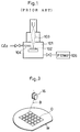
- a known focused ion beam etching apparatus has a construction as shown in Fig. 1.
- This apparatus includes a sample chamber 101 in which a wafer 102 is placed for processing, the sample chamber 101 being decompressed by an exhaust unit 105.
- the apparatus etches the wafer 102 by directing thereto a focused Ga+ ion beam 103 with an accelerating voltage of 30keV along with chlorine (Cl2) gas acting as an etching gas.
- the chlorine gas is sprayed to the wafer 102 through a fine nozzle 104.
- the present invention has been made having regard to the state of the art noted above, and its object is to provide a focused ion beam etching apparatus for etching wafers without damaging their surfaces and without contaminating a sample chamber and a wafer.
- an apparatus for effecting micro fabrication of wafer surfaces by emitting a focused ion beam thereto comprising: a vacuum chamber, a field ionization type ion source disposed in one end of the vacuum chamber and having a gas introducing pipe, an ion beam extracting device for extracting ions having a chemical etching function from the ion source and focusing the ions into an ion beam, a deflecting device for directing the ion beam in a predetermined pattern on a surface of a wafer under treatment, a decelerating device for decelerating the ion beam to a predetermined energy for impingement on the wafer surface, and a sample section disposed in the other end of the vacuum chamber for accommodating the wafer to which the ion beam is directed in deceleration.
- ions having a chemical etching function are extracted from the field ionization type ion source, focused into an ion beam, decelerated to a predetermined energy, and directed in a predetermined pattern to a wafer surface under treatment.
- the wafer surface is free from damage since the decelerated focused ion beam is used to etch the wafer surface. Moreover, since the ions having an etching function are extracted directly from the field ionization type ion source for use in etching, an etching gas need not be introduced into the sample section. Thus, the possibility of contaminating the sample section and wafer is precluded.
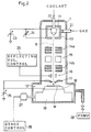
- the focused ion beam etching apparatus shown therein comprises a vacuum chamber 1.
- the vacuum chamber 1 includes a gas ion emitter 11 of the field ionization type disposed in one end region thereof, and a sample section 12 disposed in the other end region for accommodating a wafer W to be processed.
- the vacuum chamber 1 further includes a pipe 21 connected to the end region where the emitter 11 is disposed, for introducing a gas from a gas source not shown, from which ions are extracted by field ionization.
- a cooling pipe 22 is connected to the emitter 11 for supplying a cooling medium such as liquid helium to cause adsorption of the gas introduced through the pipe 21.
- the vacuum chamber 1 includes, arranged in the stated order through a region from the emitter 11 to the sample section 12, an extraction electrode 13 for extracting the ions from the emitter 11, a first electrostatic lens 14a for focusing the ions into a beam, a mass filter 15, a second electrostatic lens 14b, a deflecting electrode 16 for directing the focused ion beam in a predetermined pattern to the wafer W, and a decelerating electrode 17 for reducing the focused ion beam to a predetermined energy.
- the wafer W is placed on a sample stage 18 in the sample section 12.
- the sample stage 18 is mounted on an XY stage 19 movable on a horizontal plane.
- the focused ion beam etching apparatus in this embodiment further includes an accelerating power source 23 of about 30-50kV for applying an accelerating energy to the ions, an extraction power source 24 of several tens of kV to apply a potential difference between the emitter 11 and electrode 13, and a decelerating power source 25 of fine adjustable voltage for generating voltage up to a maximum corresponding to that of the accelerating power source 23.
- Numeral 26 in Fig. 2 denotes a deflecting voltage control unit for applying a deflecting voltage to the deflecting electrode 16.
- Numeral 27 denotes a motor for driving the XY stage 19.
- Numeral 28 denotes a stage movement control unit for controlling the motor 27.
- Numeral 29 denotes an exhaust device for decompressing the vacuum chamber 1.
- an ion beam B extracted from the ion emitter 11 is focused by the electrostatic lenses 14a and 14b, and ions are selected through the mass filter 15 for entry to the sample section 12.
- the energy of the focused ion beam B reaching the wafer W on the sample stage 18 is equal to a difference in output voltage between the accelerating power source 23 and decelerating power source 25.
- the focused ion beam B retains the energy applied by the accelerating power source 23 until the beam B approaches the decelerating electrode 17.
- the potential of the decelerating electrode 17 and sample stage 18 is increased by the decelerating power source 25, the focused ion beam B impinging on the wafer W is decelerated by an amount corresponding to the potential increase.
- the energy of the focused ion beam B reaching the wafer W may be varied steplessly by adjusting the output of the decelerating power source 25, in theory from zero output to full output of the accelerating power source 23.
- an wafer surface may be etched free from damage with the ions decelerated to a degree to cause no damage to the wafer W, e.g. to 50-100eV.
- chlorine (Cl2) gas or fluorine (SF6) gas as the ion producing gas
- chlorine ions or fluorine ions may be generated for use in etching the surface of a gallium arsenide (GaAs) wafer or a silicon (Si) wafer.
- Chlorine ions are used for the former wafer, while chlorine ions or fluorine ions are used for the latter.
- the focused ion beam itself has a chemical etching function, it is unnecessary to introduce an etching gas toward the wafer W as in the conventional apparatus. Thus, the sample section 12 and wafer W are free from contamination.
- the stage movement control unit 28 is actuated to apply a control signal to the motor 27 to move the XY stage 19.
- the wafer W is moved with the sample stage 18 to enable fine patterns to be formed on selected positions of the wafer W.
- Positions of the sample stage 18 are determined accurately by means of a measuring machine such as a laser interferometer. As shown in Fig. 3, for example, movement from one to another of numerous divisions D on the wafer W may rely on the XY stage 19, while a fine pattern may be formed within each division D by driving the deflecting electrode 16.
Landscapes
- Physics & Mathematics (AREA)
- Engineering & Computer Science (AREA)
- Plasma & Fusion (AREA)
- Chemical & Material Sciences (AREA)
- Analytical Chemistry (AREA)
- Drying Of Semiconductors (AREA)
- Particle Accelerators (AREA)
Applications Claiming Priority (2)
| Application Number | Priority Date | Filing Date | Title |
|---|---|---|---|
| JP2261516A JPH088245B2 (ja) | 1990-09-28 | 1990-09-28 | 集束イオンビームエッチング装置 |
| JP261516/90 | 1990-09-28 |
Publications (3)
| Publication Number | Publication Date |
|---|---|
| EP0477992A2 true EP0477992A2 (de) | 1992-04-01 |
| EP0477992A3 EP0477992A3 (en) | 1992-07-01 |
| EP0477992B1 EP0477992B1 (de) | 1995-12-27 |
Family
ID=17362993
Family Applications (1)
| Application Number | Title | Priority Date | Filing Date |
|---|---|---|---|
| EP91116748A Expired - Lifetime EP0477992B1 (de) | 1990-09-28 | 1991-09-30 | Ätzgerät unter Verwendung eines fokussierten Ionenstrahls |
Country Status (4)
| Country | Link |
|---|---|
| US (1) | US5518595A (de) |
| EP (1) | EP0477992B1 (de) |
| JP (1) | JPH088245B2 (de) |
| DE (1) | DE69115818T2 (de) |
Cited By (30)
| Publication number | Priority date | Publication date | Assignee | Title |
|---|---|---|---|---|
| EP0579524A1 (de) * | 1992-06-29 | 1994-01-19 | Sumitomo Electric Industries, Ltd. | Implantationsgerät mittels fokusierten Ionenstrahls |
| EP0855734A1 (de) * | 1996-12-20 | 1998-07-29 | Schlumberger Technologies, Inc. | Ätzverfahren unter Verwendung eines fokussierten Ionenstrahls mit 1,2-Dijodoäthan |
| EP1047104A1 (de) * | 1999-04-19 | 2000-10-25 | Advantest Corporation | Gerät zur partikelinduzierter Veränderung einer Probe |
| WO2001053891A1 (fr) * | 2000-01-21 | 2001-07-26 | X-Ion | Procede de lithographie ionique, revetement a fort contraste, equipement et reticule de mise en oeuvre |
| WO2001067502A3 (en) * | 2000-03-10 | 2002-02-21 | Fei Co | Method and apparatus for milling copper interconnects in a charged particle beam system |
| WO2006133241A3 (en) * | 2005-06-07 | 2007-02-15 | Alis Technology Corp | Scanning transmission ion microscope |
| WO2007067328A2 (en) | 2005-12-02 | 2007-06-14 | Alis Corporation | Ion sources, systems and methods |
| US7368727B2 (en) | 2003-10-16 | 2008-05-06 | Alis Technology Corporation | Atomic level ion source and method of manufacture and operation |
| US7414243B2 (en) | 2005-06-07 | 2008-08-19 | Alis Corporation | Transmission ion microscope |
| US7435973B2 (en) | 2002-02-25 | 2008-10-14 | Carl Zeiss Nts Gmbh | Material processing system and method |
| US7485873B2 (en) | 2003-10-16 | 2009-02-03 | Alis Corporation | Ion sources, systems and methods |
| US7488952B2 (en) | 2003-10-16 | 2009-02-10 | Alis Corporation | Ion sources, systems and methods |
| US7495232B2 (en) | 2003-10-16 | 2009-02-24 | Alis Corporation | Ion sources, systems and methods |
| US7504639B2 (en) | 2003-10-16 | 2009-03-17 | Alis Corporation | Ion sources, systems and methods |
| US7511279B2 (en) | 2003-10-16 | 2009-03-31 | Alis Corporation | Ion sources, systems and methods |
| US7511280B2 (en) | 2003-10-16 | 2009-03-31 | Alis Corporation | Ion sources, systems and methods |
| US7518122B2 (en) | 2003-10-16 | 2009-04-14 | Alis Corporation | Ion sources, systems and methods |
| US7521693B2 (en) | 2003-10-16 | 2009-04-21 | Alis Corporation | Ion sources, systems and methods |
| US7554097B2 (en) | 2003-10-16 | 2009-06-30 | Alis Corporation | Ion sources, systems and methods |
| US7554096B2 (en) | 2003-10-16 | 2009-06-30 | Alis Corporation | Ion sources, systems and methods |
| US7557359B2 (en) | 2003-10-16 | 2009-07-07 | Alis Corporation | Ion sources, systems and methods |
| US7557361B2 (en) | 2003-10-16 | 2009-07-07 | Alis Corporation | Ion sources, systems and methods |
| US7557358B2 (en) | 2003-10-16 | 2009-07-07 | Alis Corporation | Ion sources, systems and methods |
| US7557360B2 (en) | 2003-10-16 | 2009-07-07 | Alis Corporation | Ion sources, systems and methods |
| US7601953B2 (en) | 2006-03-20 | 2009-10-13 | Alis Corporation | Systems and methods for a gas field ion microscope |
| US7786452B2 (en) | 2003-10-16 | 2010-08-31 | Alis Corporation | Ion sources, systems and methods |
| US7786451B2 (en) | 2003-10-16 | 2010-08-31 | Alis Corporation | Ion sources, systems and methods |
| US7804068B2 (en) | 2006-11-15 | 2010-09-28 | Alis Corporation | Determining dopant information |
| US8110814B2 (en) | 2003-10-16 | 2012-02-07 | Alis Corporation | Ion sources, systems and methods |
| US9159527B2 (en) | 2003-10-16 | 2015-10-13 | Carl Zeiss Microscopy, Llc | Systems and methods for a gas field ionization source |
Families Citing this family (10)
| Publication number | Priority date | Publication date | Assignee | Title |
|---|---|---|---|---|
| US5693241A (en) * | 1996-06-18 | 1997-12-02 | The United States Of America As Represented By The Administrator Of The National Aeronautics And Space Administration | Atmospheric pressure method and apparatus for removal of organic matter with atomic and ionic oxygen |
| US6808606B2 (en) | 1999-05-03 | 2004-10-26 | Guardian Industries Corp. | Method of manufacturing window using ion beam milling of glass substrate(s) |
| US6368664B1 (en) | 1999-05-03 | 2002-04-09 | Guardian Industries Corp. | Method of ion beam milling substrate prior to depositing diamond like carbon layer thereon |
| US6806198B1 (en) * | 2001-05-23 | 2004-10-19 | Advanced Micro Devices, Inc. | Gas-assisted etch with oxygen |
| US20030127424A1 (en) * | 2002-01-08 | 2003-07-10 | Seagate Technology Llc | Method of fabricating magnetic recording heads using asymmetric focused-Ion-beam trimming |
| US20040063212A1 (en) * | 2002-09-30 | 2004-04-01 | Allen Pratt | Conditioning chamber for metallurgical surface science |
| US8001853B2 (en) * | 2002-09-30 | 2011-08-23 | Her Majesty The Queen In Right Of Canada, As Represented By The Minister Of Natural Resources | Conditioning chamber for metallurgical surface science |
| WO2006086090A2 (en) * | 2005-01-03 | 2006-08-17 | The Regents Of The University Of California | Method and apparatus for generating nuclear fusion using crystalline materials |
| US7205237B2 (en) * | 2005-07-05 | 2007-04-17 | International Business Machines Corporation | Apparatus and method for selected site backside unlayering of si, GaAs, GaxAlyAszof SOI technologies for scanning probe microscopy and atomic force probing characterization |
| WO2009147894A1 (ja) * | 2008-06-05 | 2009-12-10 | 株式会社日立ハイテクノロジーズ | イオンビーム装置 |
Family Cites Families (13)
| Publication number | Priority date | Publication date | Assignee | Title |
|---|---|---|---|---|
| JPS5915985B2 (ja) * | 1981-06-29 | 1984-04-12 | 日本電信電話株式会社 | 分解種選択イオンビ−ム蒸着方法 |
| USRE33193E (en) * | 1981-09-30 | 1990-04-03 | Hitachi, Ltd. | Ion beam processing apparatus and method of correcting mask defects |
| JPS58106750A (ja) * | 1981-12-18 | 1983-06-25 | Toshiba Corp | フオ−カスイオンビ−ム加工方法 |
| JPS61136229A (ja) * | 1984-12-06 | 1986-06-24 | Toshiba Corp | ドライエツチング装置 |
| JPH0682642B2 (ja) * | 1985-08-09 | 1994-10-19 | 株式会社日立製作所 | 表面処理装置 |
| JPH0734357B2 (ja) * | 1985-10-22 | 1995-04-12 | ソニー株式会社 | 集束イオンビ−ム装置用のイオンガン |
| JPS62154543A (ja) * | 1985-12-27 | 1987-07-09 | Hitachi Ltd | 荷電ビ−ム装置 |
| JPH01503580A (ja) * | 1987-05-11 | 1989-11-30 | マイクロビーム・インコーポレーテッド | 最適化した集束イオンビーム装置を用いたマスク修復 |
| US5035787A (en) * | 1987-07-22 | 1991-07-30 | Microbeam, Inc. | Method for repairing semiconductor masks and reticles |
| US4874460A (en) * | 1987-11-16 | 1989-10-17 | Seiko Instruments Inc. | Method and apparatus for modifying patterned film |
| JPH0628253B2 (ja) * | 1988-02-17 | 1994-04-13 | 工業技術院長 | エッチング方法 |
| JP2743399B2 (ja) * | 1988-09-24 | 1998-04-22 | ソニー株式会社 | 集束イオンビーム装置 |
| JPH02181923A (ja) * | 1989-01-09 | 1990-07-16 | Nec Corp | GaAs系基板のエッチング方法 |
-
1990
- 1990-09-28 JP JP2261516A patent/JPH088245B2/ja not_active Expired - Lifetime
-
1991
- 1991-09-30 EP EP91116748A patent/EP0477992B1/de not_active Expired - Lifetime
- 1991-09-30 DE DE69115818T patent/DE69115818T2/de not_active Expired - Fee Related
-
1995
- 1995-02-08 US US08/385,638 patent/US5518595A/en not_active Expired - Lifetime
Cited By (37)
| Publication number | Priority date | Publication date | Assignee | Title |
|---|---|---|---|---|
| US5422490A (en) * | 1992-06-29 | 1995-06-06 | Sumitomo Electric Industries, Ltd. | Focused ion beam implantation apparatus |
| EP0579524A1 (de) * | 1992-06-29 | 1994-01-19 | Sumitomo Electric Industries, Ltd. | Implantationsgerät mittels fokusierten Ionenstrahls |
| EP0855734A1 (de) * | 1996-12-20 | 1998-07-29 | Schlumberger Technologies, Inc. | Ätzverfahren unter Verwendung eines fokussierten Ionenstrahls mit 1,2-Dijodoäthan |
| EP1047104A1 (de) * | 1999-04-19 | 2000-10-25 | Advantest Corporation | Gerät zur partikelinduzierter Veränderung einer Probe |
| WO2001053891A1 (fr) * | 2000-01-21 | 2001-07-26 | X-Ion | Procede de lithographie ionique, revetement a fort contraste, equipement et reticule de mise en oeuvre |
| FR2804246A1 (fr) * | 2000-01-21 | 2001-07-27 | X Ion | Procede de lithographie ionique, revetement a fort contrast, equipement et reticule de mise en oeuvre |
| WO2001067502A3 (en) * | 2000-03-10 | 2002-02-21 | Fei Co | Method and apparatus for milling copper interconnects in a charged particle beam system |
| US7435973B2 (en) | 2002-02-25 | 2008-10-14 | Carl Zeiss Nts Gmbh | Material processing system and method |
| US7557360B2 (en) | 2003-10-16 | 2009-07-07 | Alis Corporation | Ion sources, systems and methods |
| US7554096B2 (en) | 2003-10-16 | 2009-06-30 | Alis Corporation | Ion sources, systems and methods |
| US7368727B2 (en) | 2003-10-16 | 2008-05-06 | Alis Technology Corporation | Atomic level ion source and method of manufacture and operation |
| US9236225B2 (en) | 2003-10-16 | 2016-01-12 | Carl Zeiss Microscopy, Llc | Ion sources, systems and methods |
| US9159527B2 (en) | 2003-10-16 | 2015-10-13 | Carl Zeiss Microscopy, Llc | Systems and methods for a gas field ionization source |
| US9012867B2 (en) | 2003-10-16 | 2015-04-21 | Carl Zeiss Microscopy, Llc | Ion sources, systems and methods |
| US7485873B2 (en) | 2003-10-16 | 2009-02-03 | Alis Corporation | Ion sources, systems and methods |
| US7488952B2 (en) | 2003-10-16 | 2009-02-10 | Alis Corporation | Ion sources, systems and methods |
| US7495232B2 (en) | 2003-10-16 | 2009-02-24 | Alis Corporation | Ion sources, systems and methods |
| US7504639B2 (en) | 2003-10-16 | 2009-03-17 | Alis Corporation | Ion sources, systems and methods |
| US7511279B2 (en) | 2003-10-16 | 2009-03-31 | Alis Corporation | Ion sources, systems and methods |
| US7511280B2 (en) | 2003-10-16 | 2009-03-31 | Alis Corporation | Ion sources, systems and methods |
| US7518122B2 (en) | 2003-10-16 | 2009-04-14 | Alis Corporation | Ion sources, systems and methods |
| US7521693B2 (en) | 2003-10-16 | 2009-04-21 | Alis Corporation | Ion sources, systems and methods |
| US7554097B2 (en) | 2003-10-16 | 2009-06-30 | Alis Corporation | Ion sources, systems and methods |
| US8748845B2 (en) | 2003-10-16 | 2014-06-10 | Carl Zeiss Microscopy, Llc | Ion sources, systems and methods |
| US7557359B2 (en) | 2003-10-16 | 2009-07-07 | Alis Corporation | Ion sources, systems and methods |
| US7557361B2 (en) | 2003-10-16 | 2009-07-07 | Alis Corporation | Ion sources, systems and methods |
| US7557358B2 (en) | 2003-10-16 | 2009-07-07 | Alis Corporation | Ion sources, systems and methods |
| US8110814B2 (en) | 2003-10-16 | 2012-02-07 | Alis Corporation | Ion sources, systems and methods |
| US7786451B2 (en) | 2003-10-16 | 2010-08-31 | Alis Corporation | Ion sources, systems and methods |
| US7786452B2 (en) | 2003-10-16 | 2010-08-31 | Alis Corporation | Ion sources, systems and methods |
| WO2006133241A3 (en) * | 2005-06-07 | 2007-02-15 | Alis Technology Corp | Scanning transmission ion microscope |
| US7321118B2 (en) | 2005-06-07 | 2008-01-22 | Alis Corporation | Scanning transmission ion microscope |
| US7414243B2 (en) | 2005-06-07 | 2008-08-19 | Alis Corporation | Transmission ion microscope |
| WO2007067328A2 (en) | 2005-12-02 | 2007-06-14 | Alis Corporation | Ion sources, systems and methods |
| EP1955356A2 (de) * | 2005-12-02 | 2008-08-13 | Alis Corporation | Ionenquellen, systeme und verfahren |
| US7601953B2 (en) | 2006-03-20 | 2009-10-13 | Alis Corporation | Systems and methods for a gas field ion microscope |
| US7804068B2 (en) | 2006-11-15 | 2010-09-28 | Alis Corporation | Determining dopant information |
Also Published As
| Publication number | Publication date |
|---|---|
| EP0477992A3 (en) | 1992-07-01 |
| DE69115818D1 (de) | 1996-02-08 |
| JPH04137728A (ja) | 1992-05-12 |
| EP0477992B1 (de) | 1995-12-27 |
| DE69115818T2 (de) | 1996-05-23 |
| JPH088245B2 (ja) | 1996-01-29 |
| US5518595A (en) | 1996-05-21 |
Similar Documents
| Publication | Publication Date | Title |
|---|---|---|
| EP0477992B1 (de) | Ätzgerät unter Verwendung eines fokussierten Ionenstrahls | |
| US4371412A (en) | Dry etching apparatus | |
| US4609428A (en) | Method and apparatus for microwave plasma anisotropic dry etching | |
| US4874460A (en) | Method and apparatus for modifying patterned film | |
| DE69301942T2 (de) | Verfahren und Gerät zur Beseitigung von Oberflächenbeschädigungen in Halbleiter-Materialien mittels Plasma-Ätzen | |
| US7550748B2 (en) | Apparatus and methods for systematic non-uniformity correction using a gas cluster ion beam | |
| JP2003521812A (ja) | ガスクラスターイオンビーム・スムーザー装置 | |
| JPH03218627A (ja) | プラズマエッチング方法及び装置 | |
| JP2006518916A (ja) | 偏向用の加速/減速ギャップ | |
| KR101631319B1 (ko) | 자기 바이어스 능동 부하 회로 및, 하전 입자 빔 처리 시스템용 관련된 전원 장치 | |
| GB1499847A (en) | Selective removal of material by sputter etching | |
| JP3582916B2 (ja) | プラズマエッチング装置 | |
| KR20240073994A (ko) | 콤팩트한 낮은 각도 이온 빔 추출 조립체 및 처리 장치 | |
| US5637538A (en) | Method and apparatus for processing a specimen | |
| US6669812B2 (en) | Apparatus and method for fabricating semiconductor device | |
| KR20190097071A (ko) | 보상된 위치에 따른 처리 장치 및 방법 | |
| JP3060613B2 (ja) | 集束イオンビーム装置、及び集束イオンビームを用いた断面加工方法 | |
| JPH0528950A (ja) | 断面加工方法及び装置 | |
| JPS63107118A (ja) | イオンビ−ム装置 | |
| JPH04272640A (ja) | 集束イオンビームエッチング装置 | |
| WO2015077424A1 (en) | Multi-step location specific process for substrate edge profile correction for gcib system | |
| JP2730269B2 (ja) | 半導体素子製造装置 | |
| JPH0618187B2 (ja) | 半導体基板の加工方法 | |
| JPH0817800A (ja) | 集束イオンビーム装置およびそれを用いた試料加工方法 | |
| JPS6134844A (ja) | 中性微細ビ−ムの照射装置 |
Legal Events
| Date | Code | Title | Description |
|---|---|---|---|
| PUAI | Public reference made under article 153(3) epc to a published international application that has entered the european phase |
Free format text: ORIGINAL CODE: 0009012 |
|
| AK | Designated contracting states |
Kind code of ref document: A2 Designated state(s): DE GB |
|
| PUAL | Search report despatched |
Free format text: ORIGINAL CODE: 0009013 |
|
| AK | Designated contracting states |
Kind code of ref document: A3 Designated state(s): DE GB |
|
| 17P | Request for examination filed |
Effective date: 19921210 |
|
| 17Q | First examination report despatched |
Effective date: 19950511 |
|
| GRAA | (expected) grant |
Free format text: ORIGINAL CODE: 0009210 |
|
| AK | Designated contracting states |
Kind code of ref document: B1 Designated state(s): DE GB |
|
| REF | Corresponds to: |
Ref document number: 69115818 Country of ref document: DE Date of ref document: 19960208 |
|
| REG | Reference to a national code |
Ref country code: GB Ref legal event code: 746 Effective date: 19960819 |
|
| PLBE | No opposition filed within time limit |
Free format text: ORIGINAL CODE: 0009261 |
|
| STAA | Information on the status of an ep patent application or granted ep patent |
Free format text: STATUS: NO OPPOSITION FILED WITHIN TIME LIMIT |
|
| 26N | No opposition filed | ||
| REG | Reference to a national code |
Ref country code: GB Ref legal event code: IF02 |
|
| PGFP | Annual fee paid to national office [announced via postgrant information from national office to epo] |
Ref country code: DE Payment date: 20040923 Year of fee payment: 14 |
|
| PGFP | Annual fee paid to national office [announced via postgrant information from national office to epo] |
Ref country code: GB Payment date: 20040929 Year of fee payment: 14 |
|
| PG25 | Lapsed in a contracting state [announced via postgrant information from national office to epo] |
Ref country code: GB Free format text: LAPSE BECAUSE OF NON-PAYMENT OF DUE FEES Effective date: 20050930 |
|
| PG25 | Lapsed in a contracting state [announced via postgrant information from national office to epo] |
Ref country code: DE Free format text: LAPSE BECAUSE OF NON-PAYMENT OF DUE FEES Effective date: 20060401 |
|
| GBPC | Gb: european patent ceased through non-payment of renewal fee |
Effective date: 20050930 |