EP0478134A2 - Méthodes et dispositifs pour réduire le bruit de couplage dans des dispositifs logiques programmables - Google Patents
Méthodes et dispositifs pour réduire le bruit de couplage dans des dispositifs logiques programmables Download PDFInfo
- Publication number
- EP0478134A2 EP0478134A2 EP91307604A EP91307604A EP0478134A2 EP 0478134 A2 EP0478134 A2 EP 0478134A2 EP 91307604 A EP91307604 A EP 91307604A EP 91307604 A EP91307604 A EP 91307604A EP 0478134 A2 EP0478134 A2 EP 0478134A2
- Authority
- EP
- European Patent Office
- Prior art keywords
- logical
- input signals
- group
- conductors
- logical input
- Prior art date
- Legal status (The legal status is an assumption and is not a legal conclusion. Google has not performed a legal analysis and makes no representation as to the accuracy of the status listed.)
- Granted
Links
Images


Classifications
-
- H—ELECTRICITY
- H03—ELECTRONIC CIRCUITRY
- H03K—PULSE TECHNIQUE
- H03K19/00—Logic circuits, i.e. having at least two inputs acting on one output; Inverting circuits
- H03K19/02—Logic circuits, i.e. having at least two inputs acting on one output; Inverting circuits using specified components
- H03K19/173—Logic circuits, i.e. having at least two inputs acting on one output; Inverting circuits using specified components using elementary logic circuits as components
- H03K19/177—Logic circuits, i.e. having at least two inputs acting on one output; Inverting circuits using specified components using elementary logic circuits as components arranged in matrix form
- H03K19/17704—Logic circuits, i.e. having at least two inputs acting on one output; Inverting circuits using specified components using elementary logic circuits as components arranged in matrix form the logic functions being realised by the interconnection of rows and columns
- H03K19/17708—Logic circuits, i.e. having at least two inputs acting on one output; Inverting circuits using specified components using elementary logic circuits as components arranged in matrix form the logic functions being realised by the interconnection of rows and columns using an AND matrix followed by an OR matrix, i.e. programmable logic arrays
-
- H—ELECTRICITY
- H03—ELECTRONIC CIRCUITRY
- H03K—PULSE TECHNIQUE
- H03K19/00—Logic circuits, i.e. having at least two inputs acting on one output; Inverting circuits
- H03K19/003—Modifications for increasing the reliability for protection
- H03K19/00346—Modifications for eliminating interference or parasitic voltages or currents
Definitions
- This invention relates to supplying the signals to a large group of conductors in close proximity to another group of conductors in such a way that coupling noise between the groups is reduced.
- this invention can be employed in supplying signals to the word lines of a Programmable Interconnect Array (PIA) in a high-density Programmable Logic Device (PLD) so as to reduce the noise coupled to the PIA bit lines by the signals on the word lines.
- PIA Programmable Interconnect Array
- PLD high-density Programmable Logic Device
- a high-density PLD may include a PIA which generally comprises one or more Electrically Programmable Read-Only Memory (EPROM) arrays in which a large number of word lines drive bit lines via selectively programmed floating-gate transistors. Typically, all of the word lines cross the bit lines so that appropriate interconnections can be made. This causes parasitic capacitance to be present between the word lines and the bit lines.
- the PIA bit lines are therefore susceptible to coupling noise generated when large numbers of PIA word lines are switched coherently (i.e., simultaneously in the same direction). For example, when a global clear signal activates, or when large binary counters roll over, many macrocell outputs change simultaneously.
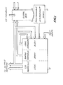
- FIG. 1 shows the architecture of a conventional high-density PLD such as the EPM5128 available from Altera Corporation of San Jose, California.
- Block 11 is the Programmable Interconnect Array (PIA) in connection with which this invention can be employed.
- FIG. 2 shows a possible circuit implementation of a conventional PIA.
- the PIA generally comprises an EPROM array with a large number of word lines 21 which are driven by outputs from macrocells and inputs from I/O pads.
- the word lines drive bit lines 22 via floating-gate transistors 23 which form EPROM bits.
- an EPROM bit is "programmed,” the associated floating-gate transistor is switched off (i.e., no channel can be induced between the source and drain).
- an EPROM bit is "erased,” a channel between the source and drain can be induced by the application of a voltage (greater than the threshold voltage) to the control gate of the transistor.
- each bit line is either driven by a selected word line through only one erased EPROM bit, or it is not driven by any word line (i.e., all EPROM bits connected to the bit line are programmed).
- the bit line voltages can easily be inadvertently disturbed by coherent switching of the word lines because the bit lines are held relatively weakly in a logical one state by a passive pull-up device, or relatively weakly in a logical zero state by a single EPROM.
- the parasitic capacitive coupling between the PIA word lines and the bit lines can result in these inadvertent disturbances being passed on as glitches to the Logic Array Block (LAB) 12 word lines 26 during coherent PIA word line switching. These glitches can cause increased delay in the sense amplifier or functional failure in the LAB logic.
- the coherent word line switching which gives rise to such glitches is fairly common in conventional PLDs, as will be described in the discussion of FIG. 4.
- the possibility of coherent switching can, however, be reduced by inverting the logical sense of some of the word lines.
- the PIA word lines, which form the input signals to the PIA are single polarity where, for the purposes of this invention, a signal is termed "single polarity" if its logical complement is not present in the logical block under consideration.
- the PIA bit lines, which form the output signals 25 from the PIA drive complementary word lines 26 in LAB 12.
- the PIA functions as a programmable switching matrix in which a selected PIA word line drives a complementary LAB word line pair. This is accomplished by programming all EPROMs on the corresponding PIA bit line except for the single EPROM corresponding to the selected PIA word line.
- FIG. 3 shows the macrocell 31 and I/O pin 32 connections of a conventional PIA.
- the FIG. shows PIA word lines 33 driven by outputs of macrocells 31, or by inputs from I/O pads 32.
- the tri-state controls 34 determine whether the I/O pads function as inputs or outputs.
- the tri-state buffers 35 pass the outputs of macrocells 31 to the I/O pads, as well as to PIA word lines 36.
- the tri-state buffers 35 isolate the I/O pads 32 from the macrocells 31. Input data is then passed from the I/O pads 32 to the PIA word lines 36.
- FIG. 4 shows various situations under which such coherent switching can occur and lead to incorrect operation of the PIA.
- Coherent switching can occur, as in FIG. 4a, with the global clearing of a large number of registers 401 containing logical ones.
- the parasitic capacitive coupling 402 from the word lines to the bit lines causes a voltage spike 403 to appear on a bit line with all EPROM bits programmed. Spikes of this form on such bit lines are possible because the bit lines are held high by a weak passive pull-up device.
- the sense amplifier 404 amplifies this spike and produces a "glitch" 405.
- Coherent switching can also occur, as in FIG. 4b, when the macrocells form parts of a large binary counter 406. As the counter is incremented, it eventually reaches a stage where a large number of the outputs are logical ones. For example, in a twelve-bit counter, the current count may be 011111111111. The occurrence of the next clock pulse causes the counter to increment its count to 100000000000. Again, the effect is for many word lines to switch coherently from logical one states to logical zero states. This phenomenon can also lead to glitches at the outputs of sense amplifiers.
- FIGS. 4a and 4b showed situations where negative-glitches can occur. However, positive glitches are also possible.
- FIG. 4c shows a possible situation in which positive glitches can occur on the output of the sense amplifier 404.
- the high on the control gate of the single erased cell 408 should ensure that bit line 407 remains low.
- Bit line 407 should not be affected by the high to low transition of SETH which causes all registers containing ones to switch to zeros, and causes a large number of lines 409 to go high simultaneously.
- the large number of lines 409 going high simultaneously causes a spike 410 on the bit line which is amplified by the sense amplifier 404 to produce the positive glitch 411.
- a single common clear signal will cause all PIA word lines to switch coherently from logical one to logical zero.
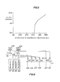
- FIG. 5 shows a plot of the glitch duration at the output of the PIA sense amplifier as a function of the effective number of coherently switching PIA word lines.
- word lines are either switching coherently or not switching. With few word lines switching coherently, the amplitude of the spike at the input of the sense amplifier may not be of sufficient magnitude to trigger that device. Only after a certain minimum number of word lines switch coherently will the output of the sense amplifier be affected.
- the critical number of word lines that need to switch coherently before a glitch occurs at the output of the sense amplifier is typically greater than 65%. This number depends on the PIA circuit and its characteristics, and the transistor characteristics of a particular process lot. In a typical architecture, about 30% of the PIA word lines are connected to I/O pads.
- the output macrocells driving I/O pins make up about 60% of PIA word lines, either as direct macrocell outputs or as I/O pad outputs. Thus, if only an additional 5% of the word lines switch coherently with the macrocells, a glitch will be obtained.
- FIG. 6 shows an illustrative embodiment of the invention designed to reduce the likelihood of coherent switching of word lines.
- the first aspect involves making the PIA output macrocell word lines (e.g., word line 608) and any associated I/O pad word lines (e.g., word line 610) to be of opposite logical sense by the introduction of invertor 618 in place of a buffer in one of these word lines.
- the two corresponding PIA word lines (608 and 610) switch in a complementary fashion, hence tending to cancel each other's effects on the bit lines.
- word lines from macrocell outputs are alternately made to be complementary to their macrocell values by the introduction of invertors (e.g., 613 and 615).
- word line 606 has the same logical value as its corresponding buried macrocell 602
- word line 607 has a logical value which is complementary to that of its corresponding buried macrocell 603. Similar statements are true regarding word lines 605 and 608, and their corresponding output macrocells 601 and 604.
- the order of the macrocells whose outputs are to be inverted is not particularly important, although the "natural order" in which circuit design software utilizes the macrocells would be preferred.
- invertor 618 is shown connected between I/O pad 620 and PIA word line 610, with other suitable modifications, it could equally well have been positioned between macrocell 604 and tri-state buffer 612.
Landscapes
- Physics & Mathematics (AREA)
- Mathematical Physics (AREA)
- Engineering & Computer Science (AREA)
- Computer Hardware Design (AREA)
- Computing Systems (AREA)
- General Engineering & Computer Science (AREA)
- Logic Circuits (AREA)
- Design And Manufacture Of Integrated Circuits (AREA)
- Read Only Memory (AREA)
Applications Claiming Priority (2)
| Application Number | Priority Date | Filing Date | Title |
|---|---|---|---|
| US587075 | 1984-03-07 | ||
| US07/587,075 US5091661A (en) | 1990-09-24 | 1990-09-24 | Methods and apparatus for reducing coupling noise in programmable logic devices |
Publications (3)
| Publication Number | Publication Date |
|---|---|
| EP0478134A2 true EP0478134A2 (fr) | 1992-04-01 |
| EP0478134A3 EP0478134A3 (en) | 1992-05-20 |
| EP0478134B1 EP0478134B1 (fr) | 1997-06-25 |
Family
ID=24348240
Family Applications (1)
| Application Number | Title | Priority Date | Filing Date |
|---|---|---|---|
| EP91307604A Expired - Lifetime EP0478134B1 (fr) | 1990-09-24 | 1991-08-16 | Méthodes et dispositifs pour réduire le bruit de couplage dans des dispositifs logiques programmables |
Country Status (4)
| Country | Link |
|---|---|
| US (1) | US5091661A (fr) |
| EP (1) | EP0478134B1 (fr) |
| JP (1) | JPH04263515A (fr) |
| DE (1) | DE69126651D1 (fr) |
Cited By (7)
| Publication number | Priority date | Publication date | Assignee | Title |
|---|---|---|---|---|
| WO2001067603A1 (fr) * | 2000-03-10 | 2001-09-13 | Multigig Limited | Generateur d'impulsions electriques et oscillateur |
| WO2001089088A1 (fr) * | 2000-05-11 | 2001-11-22 | Multigig Limited | Generateur d'impulsions electroniques et oscillateur |
| US7209065B2 (en) | 2004-07-27 | 2007-04-24 | Multigig, Inc. | Rotary flash ADC |
| US7609756B2 (en) | 2005-12-27 | 2009-10-27 | Multigig Inc. | Rotary clock flash analog to digital converter system and method |
| US7626465B2 (en) | 1999-01-22 | 2009-12-01 | Multigig Inc. | Electronic circuitry |
| US7675371B2 (en) | 1999-01-22 | 2010-03-09 | Multigig Inc. | Electronic circuitry |
| US8169267B2 (en) | 2007-03-29 | 2012-05-01 | Multigig, Inc. | Wave reversing system and method for a rotary traveling wave oscillator |
Families Citing this family (11)
| Publication number | Priority date | Publication date | Assignee | Title |
|---|---|---|---|---|
| US5332929A (en) * | 1993-04-08 | 1994-07-26 | Xilinx, Inc. | Power management for programmable logic devices |
| US5834947A (en) * | 1996-11-01 | 1998-11-10 | Waferscale Integration Inc. | Microcontroller accessible macrocell |
| US5900766A (en) * | 1997-07-11 | 1999-05-04 | Hewlett-Packard Company | Coupling charge compensation device for VLSI circuits |
| US5952846A (en) * | 1997-08-08 | 1999-09-14 | Xilinx, Inc. | Method for reducing switching noise in a programmable logic device |
| CN104205811B (zh) * | 2012-02-29 | 2019-01-25 | 索尼公司 | 列a/d转换器、列a/d转换方法、固态成像设备、和照相机系统 |
| US9256276B2 (en) | 2013-09-27 | 2016-02-09 | Intel Corporation | Utilization of processor capacity at low operating frequencies |
| US10277233B2 (en) | 2016-10-07 | 2019-04-30 | Analog Devices, Inc. | Apparatus and methods for frequency tuning of rotary traveling wave oscillators |
| US10312922B2 (en) | 2016-10-07 | 2019-06-04 | Analog Devices, Inc. | Apparatus and methods for rotary traveling wave oscillators |
| US11527992B2 (en) | 2019-09-19 | 2022-12-13 | Analog Devices International Unlimited Company | Rotary traveling wave oscillators with distributed stubs |
| US11264949B2 (en) | 2020-06-10 | 2022-03-01 | Analog Devices International Unlimited Company | Apparatus and methods for rotary traveling wave oscillators |
| US11539353B2 (en) | 2021-02-02 | 2022-12-27 | Analog Devices International Unlimited Company | RTWO-based frequency multiplier |
Family Cites Families (9)
| Publication number | Priority date | Publication date | Assignee | Title |
|---|---|---|---|---|
| JPS59212027A (ja) * | 1983-05-18 | 1984-11-30 | Toshiba Corp | 半導体集積回路の出力回路 |
| JPS6030152A (ja) * | 1983-07-28 | 1985-02-15 | Toshiba Corp | 集積回路 |
| US4774421A (en) * | 1984-05-03 | 1988-09-27 | Altera Corporation | Programmable logic array device using EPROM technology |
| JPS62214714A (ja) * | 1986-03-15 | 1987-09-21 | Fujitsu Ltd | ノイズ対策回路を備えたlsi装置 |
| US4857765A (en) * | 1987-11-17 | 1989-08-15 | International Business Machines Corporation | Noise control in an integrated circuit chip |
| US4871930A (en) * | 1988-05-05 | 1989-10-03 | Altera Corporation | Programmable logic device with array blocks connected via programmable interconnect |
| US4912342A (en) * | 1988-05-05 | 1990-03-27 | Altera Corporation | Programmable logic device with array blocks with programmable clocking |
| US4965474A (en) * | 1988-09-16 | 1990-10-23 | Texas Instruments Incorporated | Glitch suppression circuit |
| JPH0284817A (ja) * | 1988-09-20 | 1990-03-26 | Nec Corp | 集積回路 |
-
1990
- 1990-09-24 US US07/587,075 patent/US5091661A/en not_active Expired - Lifetime
-
1991
- 1991-08-16 EP EP91307604A patent/EP0478134B1/fr not_active Expired - Lifetime
- 1991-08-16 DE DE69126651T patent/DE69126651D1/de not_active Expired - Lifetime
- 1991-09-09 JP JP3228089A patent/JPH04263515A/ja active Pending
Cited By (14)
| Publication number | Priority date | Publication date | Assignee | Title |
|---|---|---|---|---|
| US8134415B2 (en) | 1999-01-22 | 2012-03-13 | Multigig, Inc. | Electronic circuitry |
| US7764130B2 (en) | 1999-01-22 | 2010-07-27 | Multigig Inc. | Electronic circuitry |
| US7675371B2 (en) | 1999-01-22 | 2010-03-09 | Multigig Inc. | Electronic circuitry |
| US7626465B2 (en) | 1999-01-22 | 2009-12-01 | Multigig Inc. | Electronic circuitry |
| WO2001067603A1 (fr) * | 2000-03-10 | 2001-09-13 | Multigig Limited | Generateur d'impulsions electriques et oscillateur |
| US7236060B2 (en) | 2000-05-11 | 2007-06-26 | Multigig Ltd. | Electronic pulse generator and oscillator |
| US7218180B2 (en) | 2000-05-11 | 2007-05-15 | Multigig, Ltd. | Low noise oscillator |
| GB2377836B (en) * | 2000-05-11 | 2004-10-27 | Multigig Ltd | Electronic pulse generator and oscillator |
| GB2377836A (en) * | 2000-05-11 | 2003-01-22 | Multigig Ltd | Electronic pulse generator and oscillator |
| WO2001089088A1 (fr) * | 2000-05-11 | 2001-11-22 | Multigig Limited | Generateur d'impulsions electroniques et oscillateur |
| US7209065B2 (en) | 2004-07-27 | 2007-04-24 | Multigig, Inc. | Rotary flash ADC |
| US7656336B2 (en) | 2004-07-27 | 2010-02-02 | Multigig Inc. | High-speed, single-slope analog-to-digital converter |
| US7609756B2 (en) | 2005-12-27 | 2009-10-27 | Multigig Inc. | Rotary clock flash analog to digital converter system and method |
| US8169267B2 (en) | 2007-03-29 | 2012-05-01 | Multigig, Inc. | Wave reversing system and method for a rotary traveling wave oscillator |
Also Published As
| Publication number | Publication date |
|---|---|
| JPH04263515A (ja) | 1992-09-18 |
| EP0478134B1 (fr) | 1997-06-25 |
| DE69126651D1 (de) | 1997-07-31 |
| US5091661A (en) | 1992-02-25 |
| EP0478134A3 (en) | 1992-05-20 |
Similar Documents
| Publication | Publication Date | Title |
|---|---|---|
| US5091661A (en) | Methods and apparatus for reducing coupling noise in programmable logic devices | |
| US4835418A (en) | Three-state bidirectional buffer | |
| US5602494A (en) | Bi-directional programmable I/O cell | |
| CA1257912A (fr) | Resaux logiques dynamiquement programmables a structure ni-ni en technologie cmos | |
| US4697107A (en) | Four-state I/O control circuit | |
| US6433600B2 (en) | Method and apparatus for glitch protection for input buffers in a source-synchronous environment | |
| US5440182A (en) | Dynamic logic interconnect speed-up circuit | |
| US5019724A (en) | Noise tolerant input buffer | |
| KR100332455B1 (ko) | 반도체 장치의 가변 임피던스 콘트롤회로 및 오프 칩 드라이버회로와 가변 임피던스 콘트롤 방법 | |
| US6864726B2 (en) | Output signal control from a DAC-driven amplifier-based driver | |
| JPH0334719A (ja) | 半導体集積回路 | |
| US5592104A (en) | Output buffer having transmission gate and isolated supply terminals | |
| US4504924A (en) | Carry lookahead logical mechanism using affirmatively referenced transfer gates | |
| US4728822A (en) | Data processing system with improved output function | |
| EP0372273B1 (fr) | Multiplexeur à portes de transfert | |
| EP0347083B1 (fr) | Configuration de porte d'attaque de sortie TTL | |
| US7355447B2 (en) | Level shifter circuit | |
| CN1096749C (zh) | 能容许5伏的输入/输出电路 | |
| US6815984B1 (en) | Push/pull multiplexer bit | |
| US5767696A (en) | Tri-state devices having exclusive gate output control | |
| KR20060103809A (ko) | 인터페이스 회로 | |
| US5329181A (en) | Complementary macrocell feedback circuit | |
| US5576636A (en) | Low power programmable logic arrays | |
| US5657276A (en) | Output stage for integrated circuits, particularly for electronic memories | |
| EP0302764B1 (fr) | Circuit pour comparer les valeurs de signaux binaires |
Legal Events
| Date | Code | Title | Description |
|---|---|---|---|
| PUAI | Public reference made under article 153(3) epc to a published international application that has entered the european phase |
Free format text: ORIGINAL CODE: 0009012 |
|
| AK | Designated contracting states |
Kind code of ref document: A2 Designated state(s): DE FR GB IT NL |
|
| PUAL | Search report despatched |
Free format text: ORIGINAL CODE: 0009013 |
|
| AK | Designated contracting states |
Kind code of ref document: A3 Designated state(s): DE FR GB IT NL |
|
| 17P | Request for examination filed |
Effective date: 19921114 |
|
| 17Q | First examination report despatched |
Effective date: 19950809 |
|
| GRAG | Despatch of communication of intention to grant |
Free format text: ORIGINAL CODE: EPIDOS AGRA |
|
| GRAH | Despatch of communication of intention to grant a patent |
Free format text: ORIGINAL CODE: EPIDOS IGRA |
|
| GRAH | Despatch of communication of intention to grant a patent |
Free format text: ORIGINAL CODE: EPIDOS IGRA |
|
| GRAA | (expected) grant |
Free format text: ORIGINAL CODE: 0009210 |
|
| AK | Designated contracting states |
Kind code of ref document: B1 Designated state(s): DE FR GB IT NL |
|
| PG25 | Lapsed in a contracting state [announced via postgrant information from national office to epo] |
Ref country code: IT Free format text: LAPSE BECAUSE OF FAILURE TO SUBMIT A TRANSLATION OF THE DESCRIPTION OR TO PAY THE FEE WITHIN THE PRE;WARNING: LAPSES OF ITALIAN PATENTS WITH EFFECTIVE DATE BEFORE 2007 MAY HAVE OCCURRED AT ANY TIME BEFORE 2007. THE CORRECT EFFECTIVE DATE MAY BE DIFFERENT FROM THE ONE RECORDED.SCRIBED TIME-LIMIT Effective date: 19970625 Ref country code: FR Effective date: 19970625 Ref country code: NL Free format text: LAPSE BECAUSE OF FAILURE TO SUBMIT A TRANSLATION OF THE DESCRIPTION OR TO PAY THE FEE WITHIN THE PRESCRIBED TIME-LIMIT Effective date: 19970625 |
|
| REF | Corresponds to: |
Ref document number: 69126651 Country of ref document: DE Date of ref document: 19970731 |
|
| PG25 | Lapsed in a contracting state [announced via postgrant information from national office to epo] |
Ref country code: DE Effective date: 19970926 |
|
| EN | Fr: translation not filed | ||
| NLV1 | Nl: lapsed or annulled due to failure to fulfill the requirements of art. 29p and 29m of the patents act | ||
| REG | Reference to a national code |
Ref country code: GB Ref legal event code: 732E |
|
| PLBE | No opposition filed within time limit |
Free format text: ORIGINAL CODE: 0009261 |
|
| STAA | Information on the status of an ep patent application or granted ep patent |
Free format text: STATUS: NO OPPOSITION FILED WITHIN TIME LIMIT |
|
| 26N | No opposition filed | ||
| REG | Reference to a national code |
Ref country code: GB Ref legal event code: IF02 |
|
| PGFP | Annual fee paid to national office [announced via postgrant information from national office to epo] |
Ref country code: GB Payment date: 20050707 Year of fee payment: 15 |
|
| GBPC | Gb: european patent ceased through non-payment of renewal fee |
Effective date: 20060816 |
|
| PG25 | Lapsed in a contracting state [announced via postgrant information from national office to epo] |
Ref country code: GB Free format text: LAPSE BECAUSE OF NON-PAYMENT OF DUE FEES Effective date: 20060816 |