EP0478890A2 - Schutzschaltung für Laserdioden - Google Patents
Schutzschaltung für Laserdioden Download PDFInfo
- Publication number
- EP0478890A2 EP0478890A2 EP91108315A EP91108315A EP0478890A2 EP 0478890 A2 EP0478890 A2 EP 0478890A2 EP 91108315 A EP91108315 A EP 91108315A EP 91108315 A EP91108315 A EP 91108315A EP 0478890 A2 EP0478890 A2 EP 0478890A2
- Authority
- EP
- European Patent Office
- Prior art keywords
- diode
- diodes
- circuit
- capacitor
- frequency
- Prior art date
- Legal status (The legal status is an assumption and is not a legal conclusion. Google has not performed a legal analysis and makes no representation as to the accuracy of the status listed.)
- Granted
Links
- 230000001681 protective effect Effects 0.000 claims abstract description 17
- 238000013016 damping Methods 0.000 claims abstract 4
- 239000003990 capacitor Substances 0.000 claims description 17
- 238000004519 manufacturing process Methods 0.000 abstract description 3
- 238000010586 diagram Methods 0.000 abstract description 2
- 238000001228 spectrum Methods 0.000 description 1
- 229910000859 α-Fe Inorganic materials 0.000 description 1
Images
Classifications
-
- H—ELECTRICITY
- H01—ELECTRIC ELEMENTS
- H01S—DEVICES USING THE PROCESS OF LIGHT AMPLIFICATION BY STIMULATED EMISSION OF RADIATION [LASER] TO AMPLIFY OR GENERATE LIGHT; DEVICES USING STIMULATED EMISSION OF ELECTROMAGNETIC RADIATION IN WAVE RANGES OTHER THAN OPTICAL
- H01S5/00—Semiconductor lasers
- H01S5/06—Arrangements for controlling the laser output parameters, e.g. by operating on the active medium
- H01S5/068—Stabilisation of laser output parameters
- H01S5/06825—Protecting the laser, e.g. during switch-on/off, detection of malfunctioning or degradation
-
- H—ELECTRICITY
- H02—GENERATION; CONVERSION OR DISTRIBUTION OF ELECTRIC POWER
- H02H—EMERGENCY PROTECTIVE CIRCUIT ARRANGEMENTS
- H02H7/00—Emergency protective circuit arrangements specially adapted for specific types of electric machines or apparatus or for sectionalised protection of cable or line systems, and effecting automatic switching in the event of an undesired change from normal working conditions
- H02H7/20—Emergency protective circuit arrangements specially adapted for specific types of electric machines or apparatus or for sectionalised protection of cable or line systems, and effecting automatic switching in the event of an undesired change from normal working conditions for electronic equipment
-
- H—ELECTRICITY
- H02—GENERATION; CONVERSION OR DISTRIBUTION OF ELECTRIC POWER
- H02H—EMERGENCY PROTECTIVE CIRCUIT ARRANGEMENTS
- H02H9/00—Emergency protective circuit arrangements for limiting excess current or voltage without disconnection
- H02H9/005—Emergency protective circuit arrangements for limiting excess current or voltage without disconnection avoiding undesired transient conditions
-
- H—ELECTRICITY
- H03—ELECTRONIC CIRCUITRY
- H03K—PULSE TECHNIQUE
- H03K17/00—Electronic switching or gating, i.e. not by contact-making and –breaking
- H03K17/08—Modifications for protecting switching circuit against overcurrent or overvoltage
- H03K17/081—Modifications for protecting switching circuit against overcurrent or overvoltage without feedback from the output circuit to the control circuit
- H03K17/0812—Modifications for protecting switching circuit against overcurrent or overvoltage without feedback from the output circuit to the control circuit by measures taken in the control circuit
- H03K17/08126—Modifications for protecting switching circuit against overcurrent or overvoltage without feedback from the output circuit to the control circuit by measures taken in the control circuit in bipolar transitor switches
Definitions
- the invention is based on a protective circuit according to the preamble of claim 1.
- Such a protective circuit known as an RF limiter, which, although it protects a laser diode from being destroyed by a high-frequency level exceeding a predetermined value, is relatively complex and expensive. In addition, the known protective circuit cannot prevent the laser diode from being destroyed by electrostatic charges.
- the invention has for its object to develop a protective circuit according to the preamble of claim 1 such that the manufacturing cost is reduced.
- the protective circuit is also intended to protect the laser diode against electrostatic charges.
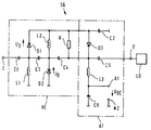
- FIG. 1 An embodiment of the invention is shown in the drawing using a single figure and is explained in more detail below.
- the figure shows a circuit diagram of the protective circuit according to the invention.
- I denotes the high-frequency input of the protective circuit SG, which is composed of a high-frequency limiting circuit BE and a high-frequency attenuation circuit AT.
- the input I is firstly connected to the anode of a first diode D1 via a first capacitor C1 and secondly to ground via a first inductor L1.
- a circuit point between the first diode D1 and the first inductor L1 is connected via a third capacitor C3 firstly to a second inductor L2 and secondly to the cathode of a second diode D2.
- a circuit point between the second inductor L2 and the second diode D2 is connected via a fourth capacitor C4 firstly with a resistor R, secondly with the cathode of a third diode D3, thirdly via a fifth capacitor C5 with the output O of the protective circuit SG and fourthly via one third inductor L3 and a sixth capacitor C6 connected in series therewith to ground.
- the ends of the first diode D1, the second inductor L2, the resistor R and the third diode D3 facing away from the capacitors C1, C3, C4, C5 are connected to ground together via a capacitor C2.
- a first terminal A1 is connected to a circuit point between the third inductance L3 and the sixth capacitor C6, and a second terminal A2 is at ground potential.
- a direct current source of voltage U DC is connected to connections A1 and A2.
- the electrostatic discharge is in the form of positive or negative voltage peaks at input I of the protective circuit SG.
- the diodes D1 and D2 are driven into the conductive state, so that the voltage pulses are limited to a harmless value U DC + U D.
- U D is the voltage drop across the diode D1 or D2.
- the third diode D3 remains without current, that is to say with high resistance.
- the first and second diodes D1 and D2 are preferably Schottky diodes, and the third diode D3 is preferably a PIN diode.
- Ferrite core coils are suitable as inductors L1 to L3.
- a protective circuit can be constructed which is suitable for high-frequency signals in a frequency range from approximately 30 MHz to over 900 MHz.
- the LC combinations L1, C1 and L2, C3 can be used to achieve a high-pass characteristic, through which the particularly high-energy, low-frequency components of the pulse spectrum are filtered out.
Landscapes
- Physics & Mathematics (AREA)
- Condensed Matter Physics & Semiconductors (AREA)
- General Physics & Mathematics (AREA)
- Electromagnetism (AREA)
- Optics & Photonics (AREA)
- Engineering & Computer Science (AREA)
- Power Engineering (AREA)
- Semiconductor Lasers (AREA)
- Emergency Protection Circuit Devices (AREA)
Abstract
Description
- Die Erfindung geht von einer Schutzschaltung nach dem Oberbegriff des Anspruchs 1 aus.
- Es ist eine derartige, als RF-Limiter bezeichnete Schutzschaltung bekannt, die eine Laserdiode zwar vor der Zerstörung durch einen einen vorgegebenen Wert überschreitenden Hochfrequenzpegel schützt, die aber verhältnismäßig kompliziert aufgebaut und teuer ist. Außerdem kann die bekannte Schutzschaltung nicht verhindern, daß die Laserdiode durch elektrostatische Aufladungen zerstört wird.
- Der Erfindung liegt die Aufgabe zugrunde, eine Schutzschaltung gemäß dem Oberbegriff des Anspruchs 1 derart weiterzubilden, daß sich der Herstellungsaufwand verringert. Außerdem soll die Schutzschaltung auch die Laserdiode vor elektrostatischen Aufladungen schützen.
- Diese Aufgabe wird bei einer Schutzschaltung gemäß dem Oberbegriff des Anspruchs 1 durch die im Kennzeichen dieses Anspruchs aufgeführten Merkmale gelöst. Die mit der Erfindung erzielbaren Vorteile bestehen insbesondere darin, daß sich die Schutzschaltung einfach und kostengünstig herstellen läßt und daß sie nicht nur auf zu hohe Hochfrequenzpegel, sondern auch auf elektrostatische Aufladungen anspricht, die die Laserdiode zerstören könnten.
- Ein Ausführungsbeispiel der Erfindung ist in der Zeichnung an Hand einer einzigen Figur dargestellt und wird im folgenden näher erläutert. Die Figur zeigt ein Schaltbild der erfindungsgemäßen Schutzschaltung.
- In der Figur bezeichnet I den Hochfrequenzeingang der Schutzschaltung SG, die sich aus einer Hochfrequenzbegrenzungsschaltung BE und einer Hochfrequenzdämpfungsschaltung AT zusammensetzt. Der Eingang I steht erstens über einen ersten Kondensator C1 mit der Anode einer ersten Diode D1 und zweitens über eine erste Induktivität L1 mit Masse in Verbindung. Ein Schaltungspunkt zwischen der ersten Diode D1 und der ersten Induktivität L1 steht über einen dritten Kondensator C3 erstens mit einer zweiten Induktivität L2 und zweitens mit der Kathode einer zweiten Diode D2 in Verbindung. Ein Schaltungspunkt zwischen der zweiten Induktivität L2 und der zweiten Diode D2 steht über einen vierten Kondensator C4 erstens mit einem Widerstand R, zweitens mit der Kathode einer dritten Diode D3, drittens über einen fünften Kondensator C5 mit dem Ausgang O der Schutzschaltung SG und viertens über eine dritte Induktivität L3 und einen damit in Serie geschalteten sechsten Kondensator C6 mit Masse in Verbindung. Die den Kondensatoren C1, C3, C4, C5 abgewandten Enden der ersten Diode D1, der zweiten Induktivität L2, des Widerstandes R und der dritten Diode D3 sind gemeinsam über einen Kondensator C2 mit Masse verbunden. Ein erster Anschluß A1 ist mit einem Schaltungspunkt zwischen der dritten Induktivität L3 und dem sechsten Kondensator C6 verbunden, und ein zweiter Anschluß A2 liegt auf dem Massepotential. An die Anschlüsse A1 und A2 ist eine Gleichstromquelle der Spannung UDC angeschlossen.
- Die Wirkungsweise der vorstehend beschriebenen Schutzschaltung ist folgende.
-
- 1.1 Hat der Pegel des am Eingang I liegenden Hochfrequenzsignals einen zulässigen Wert nicht überschritten, dann werden die Dioden D1 und D2 der Hochfrequenzbegrenzungsschaltung BE über die dritte Induktivität L3, den Widerstand R und die erste Induktivität L1 bzw. die zweite Induktivität L2 mit der Gleichspannung UDC in Sperrichtung vorgespannt. Damit sind die Dioden D1 und D2 sehr hochohmig. Die dritte Diode D3 ist stromlos und daher ebenfalls hochohmig. Der Weg für die Hochfreqenzsignale vom Eingang I zum Ausgang O der Schutzschaltung SG wird also durch die Dioden nicht beeinflußt.
- 1.2 Überschreitet der Signalpegel am Eingang I den zulässigen Wert, dann werden die Dioden D1 und D2 in positiver bzw. negativer Richtung leitend, und der Pegel der Hochfrequenzsignale wird symmetrisch auf den zulässigen Wert begrenzt. Infolge der Begrenzung fließt ein Richtstrom über die Dioden D1 und D2 durch die dritte Diode D3, wodurch diese niederohmig gesteuert wird und das Hochfrequenzsignal zusätzlich dämpft. Der Wert der Gleichspannung UDC bestimmt den Einsatzpunkt der Begrenzung.
- Die elektrostatische Entladung liegt in Form von positiven bzw. negativen Spannungsspitzen am Eingang I der Schutzschaltung SG. Dadurch werden die Dioden D1 und D2 in den leitenden Zustand gesteuert, so daß die Spannungsimpulse auf einen ungefährlichen Wert UDC + UD begrenzt werden. UD ist der Spannungsabfall über der Diode D1 bzw. D2. Die dritte Diode D3 bleibt in diesem Fall stromlos, das heißt hochohmig.
- Die erste und zweite Diode D1 und D2 sind vorzugsweise Schottky-Dioden, und die dritte Diode D3 ist vorzugsweise eine PIN-Diode. Als Induktivitäten L1 bis L3 eignen sich Ferritkernspulen. Mit den genannten Bauelementen läßt sich eine Schutzschaltung aufbauen, die für Hochfrequenzsignale eines Frequenzbereiches von etwa 30 MHz bis über 900 MHz geeignet ist. Durch die LC-Kombinationen L1, C1 und L2, C3 ist eine Hochpaßcharakteristik realisierbar, durch die die besonders energiereichen niederfrequenteren Anteile des Impulsspektrums herausgefiltert werden.
Claims (5)
- Schutzschaltung für Laserdioden, dadurch gekennzeichnet, daß die Schutzschaltung (SG) aus einer Hochfrequenzbegrenzungsschaltung (BE) mit nachgeschalteter Hochfrequenzdämpfungsschaltung (AT) besteht.
- Schutzschaltung nach Anspruch 1, dadurch gekennzeichnet, daß die Hochfrequenzbegrenzungsschaltung (BE) eine erste und eine zweite Diode (D1, D2) enthält, die auf den Hochfrequenzeingang (I) bezogen gegensinnig gepolt und durch eine Gleichspannung (UDC) in Sperrichtung vorgespannt sind, und daß die Hochfrequenzdämpfungsschaltung (AT) eine dritte Diode (D3) enthält, die ebenfalls durch die Gleichspannung (UDC) in Sperrichtung vorgespannt ist.
- Schutzschaltung nach Anspruch 1 oder 2, dadurch gekennzeichnet, daß die erste und zweite Diode (D1, D2) Schottky-Dioden sind.
- Schutzschaltung nach einem der Ansprüche 1 bis 3, dadurch gekennzeichnet, daß die dritte Diode (D3) eine PIN-Diode ist.
- Schutzschaltung nach Anspruch 1 oder einem der folgenden, dadurch gekennzeichnet, daß der Hochfrequenzeingang (I) der Schutzschaltung (SG) über einen ersten Kondensator (C1) erstens mit der Anode der ersten Diode (D1), zweitens über eine erste Induktivität (L1) mit Masse und drittens über einen dritten Kondensator (C3) erstens mit der Kathode einer zweiten Diode (D2), deren Anode auf dem Massepotential liegt, zweitens mit einer zweiten Induktivität (L2) und drittens über einen vierten Kondensator (C4) mit einem Widerstand (R) verbunden ist, daß ein Schaltungspunkt zwischen dem vierten Kondensator (C4) und dem Widerstand (R) erstens mit der Kathode der dritten Diode (D3), zweitens über eine dritte Induktivität (L3) und einen sechsten Kondensator (C6) mit Masse und drittens über einen fünften Kondensator (C5) mit dem Ausgang (O) der Schutzschaltung (SG) verbunden ist, daß die den Kondensatoren (C1, C3, C4 und C5) abgewandten Enden der ersten Diode (D1), der zweiten Induktivität (L2), des Widerstandes (R) und der dritter Diode (D3) über einen gemeinsamen zweiten Kondensator (C2) mit Masse verbunden sind und daß die Gleichspannung (UDC) zwischen Masse und einem Schaltungspunkt zwischen der dritten Induktivität (L3) und dem sechsten Kondensator (C6) liegt.
Applications Claiming Priority (2)
| Application Number | Priority Date | Filing Date | Title |
|---|---|---|---|
| DE4031066 | 1990-10-02 | ||
| DE4031066A DE4031066A1 (de) | 1990-10-02 | 1990-10-02 | Schutzschaltung fuer laserdioden |
Publications (3)
| Publication Number | Publication Date |
|---|---|
| EP0478890A2 true EP0478890A2 (de) | 1992-04-08 |
| EP0478890A3 EP0478890A3 (en) | 1993-08-11 |
| EP0478890B1 EP0478890B1 (de) | 1995-03-22 |
Family
ID=6415385
Family Applications (1)
| Application Number | Title | Priority Date | Filing Date |
|---|---|---|---|
| EP91108315A Expired - Lifetime EP0478890B1 (de) | 1990-10-02 | 1991-05-23 | Schutzschaltung für Laserdioden |
Country Status (3)
| Country | Link |
|---|---|
| US (1) | US5218612A (de) |
| EP (1) | EP0478890B1 (de) |
| DE (2) | DE4031066A1 (de) |
Cited By (1)
| Publication number | Priority date | Publication date | Assignee | Title |
|---|---|---|---|---|
| US6509779B2 (en) | 2000-01-21 | 2003-01-21 | Atheros Communications, Inc. | System for providing electrostatic discharge protection for high-speed integrated circuits |
Families Citing this family (6)
| Publication number | Priority date | Publication date | Assignee | Title |
|---|---|---|---|---|
| US5473623A (en) * | 1993-12-17 | 1995-12-05 | Quantic Industries, Inc. | Laser diode driver circuit |
| US5764667A (en) * | 1996-12-09 | 1998-06-09 | Hewlett-Packard Company | Current steering circuit |
| KR20040103289A (ko) * | 2003-06-02 | 2004-12-08 | 삼성전자주식회사 | 레이저다이오드 보호 회로 |
| CN100444384C (zh) * | 2006-01-23 | 2008-12-17 | 中国科学院微电子研究所 | 采用电感实现的射频信号集成静电释放保护电路 |
| US7646988B2 (en) * | 2006-08-04 | 2010-01-12 | Finisar Corporation | Linear amplifier for use with laser driver signal |
| US7734184B2 (en) * | 2006-08-04 | 2010-06-08 | Finisar Corporation | Optical transceiver module having an active linear optoelectronic device |
Family Cites Families (4)
| Publication number | Priority date | Publication date | Assignee | Title |
|---|---|---|---|---|
| US3806829A (en) * | 1971-04-13 | 1974-04-23 | Sys Inc | Pulsed laser system having improved energy control with improved power supply laser emission energy sensor and adjustable repetition rate control features |
| US4237427A (en) * | 1978-06-16 | 1980-12-02 | International Telephone And Telegraph Corporation | Apparatus for stabilizing a laser |
| JP2546714B2 (ja) * | 1989-02-10 | 1996-10-23 | 富士写真フイルム株式会社 | 半導体レーザ駆動回路 |
| US4924473A (en) * | 1989-03-28 | 1990-05-08 | Raynet Corporation | Laser diode protection circuit |
-
1990
- 1990-10-02 DE DE4031066A patent/DE4031066A1/de not_active Withdrawn
-
1991
- 1991-05-23 DE DE59104986T patent/DE59104986D1/de not_active Expired - Fee Related
- 1991-05-23 EP EP91108315A patent/EP0478890B1/de not_active Expired - Lifetime
- 1991-09-26 US US07/766,002 patent/US5218612A/en not_active Expired - Fee Related
Cited By (3)
| Publication number | Priority date | Publication date | Assignee | Title |
|---|---|---|---|---|
| US6509779B2 (en) | 2000-01-21 | 2003-01-21 | Atheros Communications, Inc. | System for providing electrostatic discharge protection for high-speed integrated circuits |
| US6593794B2 (en) | 2000-01-21 | 2003-07-15 | Atheros Communications | System for providing electrostatic discharge protection for high-speed integrated circuits |
| US6597227B1 (en) | 2000-01-21 | 2003-07-22 | Atheros Communications, Inc. | System for providing electrostatic discharge protection for high-speed integrated circuits |
Also Published As
| Publication number | Publication date |
|---|---|
| DE4031066A1 (de) | 1992-04-09 |
| US5218612A (en) | 1993-06-08 |
| DE59104986D1 (de) | 1995-04-27 |
| EP0478890B1 (de) | 1995-03-22 |
| EP0478890A3 (en) | 1993-08-11 |
Similar Documents
| Publication | Publication Date | Title |
|---|---|---|
| DE102009022832B4 (de) | Mehrstufige Überspannungsschutzschaltung, insbesondere für informationstechnische Anlagen | |
| EP0116275B1 (de) | Blindleistungskompensator | |
| DE2513005C3 (de) | Netzgerät zur Transformation einer ungeregelten, pulsierenden Eingangsspannung in eine stabilisierte Gleichspannung | |
| EP0769815A2 (de) | Schaltungsanordnung mit einem Schutzmittel | |
| DE3135515C2 (de) | ||
| EP0287166B1 (de) | Schaltungsanordnung zur Begrenzung der Einschaltstromspitzen bei einem Schalttransistor | |
| EP0478890B1 (de) | Schutzschaltung für Laserdioden | |
| DE4302406C2 (de) | Stromversorgungseinheit zur funkenerosiven Bearbeitung | |
| EP3952085A1 (de) | Stromrichter mit gleichtaktfilter | |
| DE2355603A1 (de) | Schutzschaltung | |
| EP0339598A2 (de) | Schutzschaltung für kapazitive Lasten | |
| EP0009811B1 (de) | Leitungsverstärker mit einer Schaltungsanordnung zum eingangs- und ausgangsseitigen Überspannungsgrobschutz | |
| DE3029697C2 (de) | ||
| DE102017106770B4 (de) | Schaltungsanordnung zum Schutz vor Netzüberspannungen für Stromrichter von Fahrzeugen, insbesondere von fahrleitungsgebundenen Fahrzeugen | |
| DE69909087T2 (de) | Verfahren zum reduzieren von verzerrungen und geräuschen von rechteckimpulsen,schaltung zum erzeugen von minimal verzerrten pulsen sowie gebrauch des verfahrens und der schaltung | |
| EP0029525B1 (de) | Stromrichterventil | |
| DE4008561C2 (de) | Verfahren zum Betreiben einer Spannungsversorgungseinrichtung für ein Elektrofilter | |
| DE2834029C2 (de) | Schutzeinrichtung gegen Überschläge in einer Senderschaltung | |
| DE3934921C1 (en) | Switching circuitry for reactive loads such as coils, and oscillators - has diode in antiparallel with each diode in series with semiconductor switch | |
| DE10245273B4 (de) | Speisegerät zur eigensicheren Energieversorgung | |
| EP0581110A2 (de) | Schaltungsanordnung zum Abbauen von Überspannungen an Transistoren | |
| DE4310233A1 (de) | Schutzschaltung für induktive Verbraucher | |
| DE3925372C2 (de) | ||
| DE10209834A1 (de) | Verfahren zur Verringerung von Störabstrahlungen bei einem DC/DC-Sperrwandler | |
| DE1512723C (de) | Dioden-Modulatorbrücke für Verstärker, welche mindestens zwei Brückenzweige aus je einer Kapazitätsdiode mit einem in Serie geschalteten niederohmigen Korrekturwiderstand enthält |
Legal Events
| Date | Code | Title | Description |
|---|---|---|---|
| PUAI | Public reference made under article 153(3) epc to a published international application that has entered the european phase |
Free format text: ORIGINAL CODE: 0009012 |
|
| AK | Designated contracting states |
Kind code of ref document: A2 Designated state(s): CH DE DK FR GB LI NL |
|
| PUAL | Search report despatched |
Free format text: ORIGINAL CODE: 0009013 |
|
| AK | Designated contracting states |
Kind code of ref document: A3 Designated state(s): CH DE DK FR GB LI NL |
|
| 17P | Request for examination filed |
Effective date: 19931214 |
|
| 17Q | First examination report despatched |
Effective date: 19940323 |
|
| GRAA | (expected) grant |
Free format text: ORIGINAL CODE: 0009210 |
|
| AK | Designated contracting states |
Kind code of ref document: B1 Designated state(s): CH DE DK FR GB LI NL |
|
| PG25 | Lapsed in a contracting state [announced via postgrant information from national office to epo] |
Ref country code: NL Free format text: LAPSE BECAUSE OF NON-PAYMENT OF DUE FEES Effective date: 19950322 Ref country code: GB Effective date: 19950322 Ref country code: FR Effective date: 19950322 Ref country code: DK Effective date: 19950322 |
|
| REF | Corresponds to: |
Ref document number: 59104986 Country of ref document: DE Date of ref document: 19950427 |
|
| PG25 | Lapsed in a contracting state [announced via postgrant information from national office to epo] |
Ref country code: LI Effective date: 19950531 Ref country code: CH Effective date: 19950531 |
|
| EN | Fr: translation not filed | ||
| NLV1 | Nl: lapsed or annulled due to failure to fulfill the requirements of art. 29p and 29m of the patents act | ||
| GBV | Gb: ep patent (uk) treated as always having been void in accordance with gb section 77(7)/1977 [no translation filed] |
Effective date: 19950322 |
|
| PLBE | No opposition filed within time limit |
Free format text: ORIGINAL CODE: 0009261 |
|
| STAA | Information on the status of an ep patent application or granted ep patent |
Free format text: STATUS: NO OPPOSITION FILED WITHIN TIME LIMIT |
|
| REG | Reference to a national code |
Ref country code: CH Ref legal event code: PL |
|
| 26N | No opposition filed | ||
| PGFP | Annual fee paid to national office [announced via postgrant information from national office to epo] |
Ref country code: DE Payment date: 19960723 Year of fee payment: 6 |
|
| PG25 | Lapsed in a contracting state [announced via postgrant information from national office to epo] |
Ref country code: DE Free format text: LAPSE BECAUSE OF NON-PAYMENT OF DUE FEES Effective date: 19980203 |