EP0479552A2 - Anzeigegerät - Google Patents
Anzeigegerät Download PDFInfo
- Publication number
- EP0479552A2 EP0479552A2 EP91308979A EP91308979A EP0479552A2 EP 0479552 A2 EP0479552 A2 EP 0479552A2 EP 91308979 A EP91308979 A EP 91308979A EP 91308979 A EP91308979 A EP 91308979A EP 0479552 A2 EP0479552 A2 EP 0479552A2
- Authority
- EP
- European Patent Office
- Prior art keywords
- scanning
- scanning signal
- lines
- signal
- signal lines
- Prior art date
- Legal status (The legal status is an assumption and is not a legal conclusion. Google has not performed a legal analysis and makes no representation as to the accuracy of the status listed.)
- Granted
Links
Images


Classifications
-
- G—PHYSICS
- G09—EDUCATION; CRYPTOGRAPHY; DISPLAY; ADVERTISING; SEALS
- G09G—ARRANGEMENTS OR CIRCUITS FOR CONTROL OF INDICATING DEVICES USING STATIC MEANS TO PRESENT VARIABLE INFORMATION
- G09G3/00—Control arrangements or circuits, of interest only in connection with visual indicators other than cathode-ray tubes
- G09G3/20—Control arrangements or circuits, of interest only in connection with visual indicators other than cathode-ray tubes for presentation of an assembly of a number of characters, e.g. a page, by composing the assembly by combination of individual elements arranged in a matrix no fixed position being assigned to or needed to be assigned to the individual characters or partial characters
- G09G3/34—Control arrangements or circuits, of interest only in connection with visual indicators other than cathode-ray tubes for presentation of an assembly of a number of characters, e.g. a page, by composing the assembly by combination of individual elements arranged in a matrix no fixed position being assigned to or needed to be assigned to the individual characters or partial characters by control of light from an independent source
- G09G3/36—Control arrangements or circuits, of interest only in connection with visual indicators other than cathode-ray tubes for presentation of an assembly of a number of characters, e.g. a page, by composing the assembly by combination of individual elements arranged in a matrix no fixed position being assigned to or needed to be assigned to the individual characters or partial characters by control of light from an independent source using liquid crystals
- G09G3/3611—Control of matrices with row and column drivers
- G09G3/3674—Details of drivers for scan electrodes
- G09G3/3677—Details of drivers for scan electrodes suitable for active matrices only
-
- G—PHYSICS
- G09—EDUCATION; CRYPTOGRAPHY; DISPLAY; ADVERTISING; SEALS
- G09G—ARRANGEMENTS OR CIRCUITS FOR CONTROL OF INDICATING DEVICES USING STATIC MEANS TO PRESENT VARIABLE INFORMATION
- G09G3/00—Control arrangements or circuits, of interest only in connection with visual indicators other than cathode-ray tubes
- G09G3/20—Control arrangements or circuits, of interest only in connection with visual indicators other than cathode-ray tubes for presentation of an assembly of a number of characters, e.g. a page, by composing the assembly by combination of individual elements arranged in a matrix no fixed position being assigned to or needed to be assigned to the individual characters or partial characters
- G09G3/34—Control arrangements or circuits, of interest only in connection with visual indicators other than cathode-ray tubes for presentation of an assembly of a number of characters, e.g. a page, by composing the assembly by combination of individual elements arranged in a matrix no fixed position being assigned to or needed to be assigned to the individual characters or partial characters by control of light from an independent source
- G09G3/36—Control arrangements or circuits, of interest only in connection with visual indicators other than cathode-ray tubes for presentation of an assembly of a number of characters, e.g. a page, by composing the assembly by combination of individual elements arranged in a matrix no fixed position being assigned to or needed to be assigned to the individual characters or partial characters by control of light from an independent source using liquid crystals
- G09G3/3611—Control of matrices with row and column drivers
- G09G3/3648—Control of matrices with row and column drivers using an active matrix
- G09G3/3659—Control of matrices with row and column drivers using an active matrix the addressing of the pixel involving the control of two or more scan electrodes or two or more data electrodes, e.g. pixel voltage dependant on signal of two data electrodes
-
- G—PHYSICS
- G09—EDUCATION; CRYPTOGRAPHY; DISPLAY; ADVERTISING; SEALS
- G09G—ARRANGEMENTS OR CIRCUITS FOR CONTROL OF INDICATING DEVICES USING STATIC MEANS TO PRESENT VARIABLE INFORMATION
- G09G2310/00—Command of the display device
- G09G2310/02—Addressing, scanning or driving the display screen or processing steps related thereto
- G09G2310/0202—Addressing of scan or signal lines
- G09G2310/0205—Simultaneous scanning of several lines in flat panels
-
- G—PHYSICS
- G09—EDUCATION; CRYPTOGRAPHY; DISPLAY; ADVERTISING; SEALS
- G09G—ARRANGEMENTS OR CIRCUITS FOR CONTROL OF INDICATING DEVICES USING STATIC MEANS TO PRESENT VARIABLE INFORMATION
- G09G2310/00—Command of the display device
- G09G2310/02—Addressing, scanning or driving the display screen or processing steps related thereto
- G09G2310/0224—Details of interlacing
-
- G—PHYSICS
- G09—EDUCATION; CRYPTOGRAPHY; DISPLAY; ADVERTISING; SEALS
- G09G—ARRANGEMENTS OR CIRCUITS FOR CONTROL OF INDICATING DEVICES USING STATIC MEANS TO PRESENT VARIABLE INFORMATION
- G09G2310/00—Command of the display device
- G09G2310/02—Addressing, scanning or driving the display screen or processing steps related thereto
- G09G2310/0264—Details of driving circuits
- G09G2310/0281—Arrangement of scan or data electrode driver circuits at the periphery of a panel not inherent to a split matrix structure
-
- G—PHYSICS
- G09—EDUCATION; CRYPTOGRAPHY; DISPLAY; ADVERTISING; SEALS
- G09G—ARRANGEMENTS OR CIRCUITS FOR CONTROL OF INDICATING DEVICES USING STATIC MEANS TO PRESENT VARIABLE INFORMATION
- G09G2320/00—Control of display operating conditions
- G09G2320/02—Improving the quality of display appearance
- G09G2320/0204—Compensation of DC component across the pixels in flat panels
-
- G—PHYSICS
- G09—EDUCATION; CRYPTOGRAPHY; DISPLAY; ADVERTISING; SEALS
- G09G—ARRANGEMENTS OR CIRCUITS FOR CONTROL OF INDICATING DEVICES USING STATIC MEANS TO PRESENT VARIABLE INFORMATION
- G09G2320/00—Control of display operating conditions
- G09G2320/02—Improving the quality of display appearance
- G09G2320/0219—Reducing feedthrough effects in active matrix panels, i.e. voltage changes on the scan electrode influencing the pixel voltage due to capacitive coupling
Definitions
- This invention relates to a display apparatus such as a liquid crystal display (LCD) apparatus, and more particularly to an active matrix LCD apparatus.
- LCD liquid crystal display
- FIG. 13 diagrammatically shows an active matrix LCD apparatus which uses thin-film transistors (TFTs) as switching devices and in which two scanning signal lines are simultaneously scanned (hereinafter, this scanning method is referred to as "two-line simultaneous scanning method").
- This TFT active matrix LCD apparatus comprises a large number of scanning signal lines 13 and data signal lines 14 formed on a substrate 11 which cross at right angles, and a matrix array of pixel electrodes 12 connected to these signal lines 13 and 14 via TFTs 15.
- a common opposite electrode (not shown) is disposed opposite to the TFT active matrix substrate with a liquid crystal layer interposed therebetween.
- the selection signal is applied to two adjacent scanning signal lines 13 at the same time.
- the selection signal is first applied simultaneously to the first and second scanning signal lines 13, and then, after one horizontal scanning period, to the third and fourth scanning lines 13.
- the selection signal is sequentially applied to each pair of an odd-numbered scanning signal line 13 and the succeeding even-numbered scanning signal line 13.
- the selection signal is first applied to the first scanning signal line 13, and then, after one horizontal scanning period, the selection signal is applied simultaneously to the second and third scanning signal lines 13, and thereafter to the fourth and fifth scanning signal lines 13.
- the selection signal is simultaneously applied to two adjacent scanning signal lines 13 paired differently from when scanning an odd-numbered field.
- the two-line simultaneous scanning method requires two times more scanning signal lines 13 and pixel electrodes 12, but can produce a high-resolution image conforming to the interlaced scanning system.
- the two-line simultaneous scanning method is described in detail in U.S. patent application serial No. 07/476,536 filed on February 7, 1990 and EPC patent application No. 90301414.0 filed on February 9, 1990. These are incorporated herein as references.
- the potential at each of the pixel electrodes 12 connected to the scanning signal lines 13 to which the selection signal has been applied drops to a lower level than the data signal potential because of the effect of a parasitic capacitance Cg d between the gate and drain of the activated TFT 15.
- the gate voltages at the activation and inactivation of the TFT 15 are denoted as V GH and V GL , respectively, and the capacitance of the liquid crystal layer at the pixel electrode 12 is denoted as C Lc
- the potential drops below the data signal potential approximately by the potential AV indicated by the following expression (1).
- the effect of a stray capacitance Cpg between the pixel electrode and a scanning signal line not connected but adjacent to the pixel electrode must also be considered in addition to the parasitic capacitance Cg d . That is, when selection signals Sa and Sb are applied to scanning signal lines 13a and 13b, as shown in Figure 15, thereby selecting the rows to which pixel electrodes 12a and 12b are connected, the pixel electrode 12a disposed between the scanning signal lines 13a and 13b and connected to the scanning signal line 13a experiences a potential drop AV1 indicated by the following expression (2), when the application of the selection signal Sa is completed. This is because the scanning signal line 13b which is not connected but adjacent to the pixel electrode 12a also experiences a potential variation as the selection signal Sb is applied to it.
- the potential drop ⁇ V2 at the pixel electrode 12b is indicated by the following expression (3).
- the pixel electrodes 12a and 12b are connected to the same data signal line 14 and supplied with the same data signal voltage, a difference arises between the potential drops AV1 and AV2 when the application of the selection signal is completed, and thereafter the pixel electrode 12b retains a higher potential.
- a prior art liquid crystal display has the problem that when the selection signal is applied simultaneously to a plurality of scanning signal lines, there occurs a difference in brightness between adjacent pixels on the same data signal line, resulting in a degradation in the image quality.
- the display apparatus of this invention which overcomes the above-discussed and numerous other disadvantages and deficiencies of the prior art, comprises: a display panel having scanning signal lines arranged in parallel, data signal lines, switching elements which are controlled by a signal supplied through said scanning signal lines, pixel electrodes connected to said data signal lines through said switching elements; and drive means for simultaneously applying said signal to at least two succeeding ones of said scanning signal lines, and said drive means comprises timing control means for terminating the application of said signal to one of said at least two scanning signal lines earlier than the application of said signal to another one of said at least two scanning signal lines.
- said one scanning signal line is disposed between a pixel electrode to which said one scanning signal line is connected and another pixel electrode to which said other one scanning signal line is connected.
- said drive means comprises clock signal means for supplying at least two clock signals which are phase-shifted from each other.
- selection signals Sa and Sb are respectively applied to scanning signal lines 13a and 13b at the same time, and the selection signal Sb is terminated faster (at time t 1 ) which is applied to the scanning signal line 13b disposed between two pixel electrodes 12a and 12b which are respectively connected to the scanning signal lines 13a and 13b. Since there is no variation in the potential of the scanning signal line 13c, the potential drop AV at the pixel electrode 12b in this case has the value indicated by above-mentioned expression (3).
- the potential of the pixel electrode 12a which is adjacent through the stray capacitance Cpg is also affected by this termination so as to decrease once. Since the TFT 15 remains conductive at this time and the pixel electrode 12a is connected to the data signal line 14, however, the pixel electrode 12a is immediately charged so as to return to the potential of the data signal.
- the application of the selection signal Sa for the scanning signal line 13a is terminated at time t 2 .
- the potential change at the adjacent scanning signal line 13b has already ended. Therefore, the potential drop AV at the pixel electrode 12a changes in the same manner as that of the pixel electrode 12b, and the potential drop AV has a value indicated by expression (4).
- the potentials of pixel electrodes connected to the two scanning signal lines drop in the same degree so that these pixel electrodes have the same potential, whereby a uniform display can be attained.
- the display apparatus comprises: a display panel having scanning signal lines arranged in parallel, data signal lines, switching elements which are controlled by a signal supplied through said scanning signal lines, pixel electrodes connected to said data signal lines through said switching elements; and drive means for simultaneously applying said signal to at least two succeeding ones of said scanning signal lines, and said drive means comprises voltage means for making the level of said signal applied to one of said at least two scanning signal lines higher than the level of said signal applied to another one of said at least two scanning signal lines.
- said one scanning signal line is disposed between a pixel electrode to which said one scanning signal line is connected and another pixel electrode to which said other one scanning signal line is connected.
- selection signals Sa and Sb are respectively applied to scanning signal lines 13a and 13b at the same time.
- the level V GH 2 of the selection signal Sb applied to the scanning signal line 13b which is disposed between pixel electrodes 12a and 12b is higher than the level V GH 1 of the selection signal Sa applied to the scanning signal line 13a.
- These voltage levels V GH 1 and V GH 2 are selected so as to be sufficiently higher than the threshold value of the TFTs 15a and 15b.
- the potentials at the pixel electrodes 12a and 12b drop due to the coupling caused by the parasitic capacitance Cg d and stray capacitance Cpg.
- the potential drops ⁇ V1' and AV2' at the pixel electrodes 12a and 12b take the values indicated by the following expressions (5) and (6), respectively.
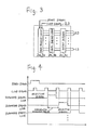
- FIG. 2 shows an embodiment of the invention.
- This embodiment is a TFT active matrix LCD apparatus which is useful in a color television receiver for the NTSC (National Television System Committee) standard.
- This embodiment comprises a TFT active liquid crystal panel 1 on which, in the same manner as shown in Figure 13, large numbers of pixel electrodes 12a, 12b, ⁇ , scanning signal lines 13a, 13b, ⁇ , data signal lines 14, and TFTs 15a, 15b, ... are formed.
- Each of the pixel electrodes 12a, 12b, ... is connected to the adjacent data signal line 14 via the respective TFT 15a, 15b, ⁇ .
- the gate of each of the TFTs 15a, 15b, ⁇ is connected to the adjacent scanning signal line 13a, 13b, ....
- a selection signal of a high level is applied to one of the scanning signal lines 13a, 13b, ⁇ , the TFT connected to that scanning signal line becomes conductive.
- the scanning signal lines 13a, 13b, ... are arranged in such a way that the even-numbered lines and the odd-numbered lines are directed in opposite directions to each other, as shown in Figure 2.
- the odd-numbered scanning signal lines 13a, 13c, ... are connected to a scanning signal line drive circuit 2, while the even-numbered scanning signal lines 13b, 13d, ... are connected to another scanning signal line drive circuit 3.
- the scanning signal line drive circuits 2 and 3 comprise a shift register circuit 2a, 3a for shifting a start signal in response to a clock signal, a level shifter circuit 2b, 3b for raising the output of the shift register circuit 2a, 3a to a level necessary to drive the TFTs, and an output buffer 2c, 3c for holding the output of the level shifter circuit 2b, 3b and outputting it to the scanning signal lines.
- a timing control circuit 4 produces a start signal from which the selection signal is created and a clock signal which defines one horizontal scanning period, and supplies them to the shift register circuits 2a and 3a.
- the timing control circuit 4 outputs the start signal and clock signal in response to a synchronizing signal separated from the video signal.
- the start signal is output in synchronism with a vertical synchronizing signal and is supplied simultaneously to the scanning signal line drive circuits 2 and 3 in an odd-numbered field.
- the start signal supplied to the scanning signal line drive circuit 2 is delayed by one horizontal scanning period to supply to the scanning signal line drive circuit 3.
- the selection signal generated by sequentially shifting the start signal is successively output with a delay of one horizontal scanning period to the scanning signal lines 13a, 13b, - connected to the scanning signal line drive circuits 2 and 3.
- selection signals which are obtained by sequentially shifted the start signal by one horizontal scanning period are supplied to the scanning lines.
- Each of the selection signal rises in synchronism with the falling of the preceding clock signal and falls in synchronism with the rising of the succeeding clock signal.
- the timing control circuit 4 outputs the clock signal in the manner described below.
- the phase of the clock signal supplied to the scanning signal line drive circuit 3 slightly leads that of the clock signal supplied to the scanning signal line drive circuit2
- the phase of the clock signal supplied to the scanning signal line drive circuit 3 is slightly delayed from that of the clock signal supplied to the scanning signal line drive circuit 2.
- the start signal is supplied simultaneously to the scanning signal line drive circuits 2 and 3. Therefore, the selection signal is first applied simultaneously to the first and second scanning signal lines 13aand 13b, and after one horizontal scanning period to the scanning signal lines 13c and 13d. Thereafter, the selection signal is applied sequentially to each pair of an odd-numbered scanning line and the succeeding even-numbered scanning line.
- the start signal is first fed to the scanning signal line drive circuit 2 from the timing control circuit 4, and after one horizontal scanning period, the start signal is supplied to the scanning signal line drive circuit 3.
- the selection signal is first applied to the first scanning signal line 13a, and after one horizontal scanning period the selection signal is applied simultaneously to the second and third scanning signal lines 13b and 13c, and then to the scanning signal lines 13d and 13e, the selection signal thus being applied to each pair of an even-numbered line and the succeeding odd-numbered line.
- the pixels in the liquid crystal panel 1 are activated so that in an odd field the odd-numbered scanning lines each paired with the succeeding even-numbered scanning line are displayed while in an even field the even-numbered scanning lines each paired with the succeeding odd-numbered scanning line are displayed, thereby accomplishing the display of a high-resolution image by the two-line simultaneous scanning method conforming to the interlaced scanning system.
- the phase of the clock signal supplied to the scanning signal line drive circuit 3 is slightly advanced as described above.
- the application of the selection signal to an even-numbered scanning signal line starts and terminates earlier than that to an odd-numbered scanning signal lines.
- the scanning signal line 13a shown in Figure 1 corresponds to an odd-numbered scanning signal line
- the scanning signal line 13b shown in Figure 1 to an even-numbered scanning signal line.
- the potential of a pixel electrode (12b in Figure 1) connected to an even-numbered line (13b in Figure 1) on which the application of the selection signal terminates earlier is lowered from the potential of a data signal by the potential drop AV indicated by expression (4), because the potential of the adjacent scanning signal line (13c in Figure 1) does not change.
- the phase of the clock signal supplied to the scanning signal line drive circuit 3 is slightly delayed.
- the application of the selection signal to an odd-numbered scanning signal line starts and terminates earlier than that to an even-numbered scanning signal lines.
- the scanning signal line 13a shown in Figure 1 corresponds to an even-numbered scanning signal line and the scanning signal line 13b shown in Figure 1 to an odd-numbered scanning signal line.
- the potential of a pixel electrode (12b in Figure 1) connected to an odd-numbered line (13b in Figure 1) on which the application of the selection signal terminates earlier is lowered from the potential of a data signal by the degree same as the potential drop AV indicated by expression (4), because the potential of the adjacent scanning signal line (13c in Figure 1) does not change.
- the potential drop at the end of the application of the selection signal is equal at each pixel electrode on every scanning line, thereby allowing every pixel electrode to retain the same potential and thus accomplishing the display of a uniform image.
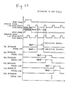
- the timing of the rising of the selection signal may be slightly different in accordance with the timing of the falling of the selection signal.
- the invention is also applicable to the case that three or more scanning lines are simultaneously supplied with a selection signal. In this case, the timing of terminating the application of a selection signal is sequentially shifted for each pair of adjacent two lines of these scanning lines.
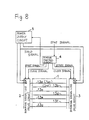
- FIG 8 shows another embodiment of the invention.
- This embodiment further comprises a power supply circuit 5.
- the selection signal When the selection signal is activated, a higher voltage V H is selected, and, when the selection signal is not activated, a lower voltage V L is selected.
- the timings of supplying the clock signal to the scanning signal line drive circuits 2 and 3 are the same.
- the powersup- ply circuit 5 receives a field signal indicative of the current field, and changes the level of the higher voltage V H in accordance with the field signal. Namely, during an odd field, the power supply circuit 5 supplies a voltage V GH 1 to the scanning signal line drive circuit 2, and a voltage V GH 2 (higher than the voltage V GH 1) to the scanning signal line drive circuit 3.
- the voltage V GH 2 is supplied to the scanning signal line drive circuit 2, and the voltage V GH 1 supplied to the scanning signal line drive circuit 3.
- the voltages V GH 1 and V GH 2 are predetermined so that the relationship expressed by foregoing expression (7) can be established among the parasitic capacitance Cg d between the gate and drain of the associated TFT 15, the stray capacitance Cpg, and the value V GL of the source voltage V L applied to the scanning signal line drive circuits 2 and 3 (the voltage applied to the scanning signal lines 13a, 13b, ⁇ during the non-activation of the selection signal).
- the potential retained at the pixel electrode 12a and that retained at the pixel electrode 12b after the completion of the application of the selection signal are both lower than the data signal potential by the potential drops AV1' and AV2' respectively indicated by expressions (5) and (6).
- AV1' AV2'
- the pixel electrodes 12a and 12b retain the potential of the same value.
- the selection signal applied simultaneously to each pair of scanning signal lines 13a, 13b, ⁇ provides a highervoltage to the odd-numbered scanning lines 13a, 13c, ... than to the even-numbered scanning lines 13b, 13d, ⁇ .
- the potential retained at the pixel electrode 12a and that retained at the pixel electrode 12b after the completion of the application of the selection signal are both lower than the data signal potential by the potential drops ⁇ V2' and AV1'.
- ⁇ V1' ⁇ 2', and therefore the pixel electrodes 12a and 12b retain the potential of the same value.
- the potential drop at the end of the application of the selection signal can be made equal between the scanning signal lines, allowing the pixel electrodes to retain the potentials of the same value and thereby accomplishing the display of a uniform image.
Landscapes
- Engineering & Computer Science (AREA)
- Chemical & Material Sciences (AREA)
- Crystallography & Structural Chemistry (AREA)
- Physics & Mathematics (AREA)
- Computer Hardware Design (AREA)
- General Physics & Mathematics (AREA)
- Theoretical Computer Science (AREA)
- Liquid Crystal Display Device Control (AREA)
- Liquid Crystal (AREA)
Applications Claiming Priority (4)
| Application Number | Priority Date | Filing Date | Title |
|---|---|---|---|
| JP2264578A JP2625248B2 (ja) | 1990-10-01 | 1990-10-01 | 液晶表示装置 |
| JP264578/90 | 1990-10-01 | ||
| JP7193091A JP2633405B2 (ja) | 1991-04-04 | 1991-04-04 | 液晶表示装置 |
| JP71930/90 | 1991-04-04 |
Publications (3)
| Publication Number | Publication Date |
|---|---|
| EP0479552A2 true EP0479552A2 (de) | 1992-04-08 |
| EP0479552A3 EP0479552A3 (en) | 1993-04-21 |
| EP0479552B1 EP0479552B1 (de) | 1997-04-16 |
Family
ID=26413052
Family Applications (1)
| Application Number | Title | Priority Date | Filing Date |
|---|---|---|---|
| EP91308979A Expired - Lifetime EP0479552B1 (de) | 1990-10-01 | 1991-10-01 | Anzeigegerät |
Country Status (4)
| Country | Link |
|---|---|
| US (1) | US5206634A (de) |
| EP (1) | EP0479552B1 (de) |
| KR (1) | KR950003345B1 (de) |
| DE (1) | DE69125679T2 (de) |
Cited By (8)
| Publication number | Priority date | Publication date | Assignee | Title |
|---|---|---|---|---|
| EP0525852A1 (de) * | 1991-07-09 | 1993-02-03 | Koninklijke Philips Electronics N.V. | Wiedergabeanordnung |
| US5841313A (en) * | 1995-08-30 | 1998-11-24 | Cherry Semiconductor Corporation | Switch with programmable delay |
| WO2002101709A1 (en) * | 2001-06-08 | 2002-12-19 | Koninklijke Philips Electronics N.V. | Addressing an array of display elements |
| DE19801263C2 (de) * | 1997-05-31 | 2003-08-21 | Lg Semicon Co Ltd | Niederleistung-Gate-Ansteuerschaltung für Dünnfilmtransistor-Flüssigkristallanzeige unter Verwendung einer elektrischen Ladungs-Recyclingtechnik |
| EP1187091A3 (de) * | 2000-09-08 | 2004-05-12 | Oh-Kyong Kwon | Verfahren zur Steuerung von Abtastzeilen in einem Flüssigkristallgerät mit aktiver Matrix |
| KR100757766B1 (ko) * | 2002-01-17 | 2007-09-12 | 레노보 (싱가포르) 피티이. 엘티디. | 표시 장치 및 주사선용 드라이버 회로 |
| EP2023331A1 (de) * | 2007-08-07 | 2009-02-11 | Samsung Electronics Co., Ltd. | Anzeigevorrichtung und Verfahren zu ihrer Ansteuerung |
| CN101996602A (zh) * | 2010-10-15 | 2011-03-30 | 深圳市华星光电技术有限公司 | 液晶显示器及其驱动显示方法 |
Families Citing this family (22)
| Publication number | Priority date | Publication date | Assignee | Title |
|---|---|---|---|---|
| EP0382567B1 (de) * | 1989-02-10 | 1996-05-29 | Sharp Kabushiki Kaisha | Flüssigkristallanzeigeeinheit und Steuerverfahren dafür |
| US5877738A (en) * | 1992-03-05 | 1999-03-02 | Seiko Epson Corporation | Liquid crystal element drive method, drive circuit, and display apparatus |
| KR950006330B1 (ko) * | 1992-04-30 | 1995-06-14 | 삼성전관주식회사 | 플라즈마 어드레스 방식의 액정표시소자 및 구동방법 |
| WO1994024660A1 (fr) * | 1993-04-09 | 1994-10-27 | Citizen Watch Co., Ltd. | Dispositif d'affichage a cristaux liquides |
| JP2671772B2 (ja) * | 1993-09-06 | 1997-10-29 | 日本電気株式会社 | 液晶ディスプレイとその駆動方法 |
| JP3298301B2 (ja) * | 1994-04-18 | 2002-07-02 | カシオ計算機株式会社 | 液晶駆動装置 |
| US6229516B1 (en) * | 1995-12-30 | 2001-05-08 | Samsung Electronics Co., Ltd. | Display a driving circuit and a driving method thereof |
| GB2314664A (en) | 1996-06-27 | 1998-01-07 | Sharp Kk | Address generator,display and spatial light modulator |
| TW556145B (en) * | 2000-01-11 | 2003-10-01 | Toshiba Corp | Flat display apparatus having scan-line driving circuit and its driving method |
| KR100367015B1 (ko) * | 2000-12-29 | 2003-01-09 | 엘지.필립스 엘시디 주식회사 | 액정 표시장치의 구동방법 |
| JP3750731B2 (ja) * | 2001-03-02 | 2006-03-01 | セイコーエプソン株式会社 | 表示パネル駆動回路及び画像表示装置 |
| TW559771B (en) * | 2001-07-23 | 2003-11-01 | Hitachi Ltd | Matrix-type display device |
| JP3947848B2 (ja) * | 2003-06-12 | 2007-07-25 | セイコーエプソン株式会社 | 電気光学装置及び電子機器 |
| TWI239424B (en) * | 2003-10-15 | 2005-09-11 | Hannstar Display Corp | Liquid crystal display panel and driving method therefor |
| US6980182B1 (en) * | 2003-10-22 | 2005-12-27 | Rockwell Collins | Display system |
| JP2005202801A (ja) * | 2004-01-16 | 2005-07-28 | Sharp Corp | 表示装置 |
| JP2006058770A (ja) * | 2004-08-23 | 2006-03-02 | Toshiba Matsushita Display Technology Co Ltd | 表示装置の駆動回路 |
| KR101365055B1 (ko) | 2006-12-04 | 2014-02-19 | 삼성디스플레이 주식회사 | 표시 장치 |
| KR101931335B1 (ko) * | 2012-03-23 | 2018-12-20 | 엘지디스플레이 주식회사 | 액정표시장치의 레벨 시프터 |
| JP2015043008A (ja) | 2013-08-26 | 2015-03-05 | 株式会社ジャパンディスプレイ | 有機el表示装置 |
| CN104834116B (zh) * | 2015-05-26 | 2019-01-25 | 深圳市华星光电技术有限公司 | 一种液晶显示面板及其驱动方法 |
| JP2019152814A (ja) * | 2018-03-06 | 2019-09-12 | シャープ株式会社 | 走査信号線駆動回路、それを備えた表示装置、および、走査信号線の駆動方法 |
Family Cites Families (5)
| Publication number | Priority date | Publication date | Assignee | Title |
|---|---|---|---|---|
| FR2485846A1 (fr) * | 1980-06-27 | 1981-12-31 | Thomson Csf | Systeme de television a haute definition |
| JPS61117599A (ja) * | 1984-11-13 | 1986-06-04 | キヤノン株式会社 | 映像表示装置のスイツチングパルス |
| EP0287055B1 (de) * | 1987-04-15 | 1993-09-29 | Sharp Kabushiki Kaisha | Flüssigkristallanzeigegerät |
| FR2635902B1 (fr) * | 1988-08-26 | 1990-10-12 | Thomson Csf | Procede de commande tres rapide par adressage semi-selectif et adressage selectif d'un panneau a plasma alternatif a entretien coplanaire |
| EP0382567B1 (de) * | 1989-02-10 | 1996-05-29 | Sharp Kabushiki Kaisha | Flüssigkristallanzeigeeinheit und Steuerverfahren dafür |
-
1991
- 1991-09-30 US US07/771,454 patent/US5206634A/en not_active Expired - Lifetime
- 1991-10-01 DE DE69125679T patent/DE69125679T2/de not_active Expired - Fee Related
- 1991-10-01 EP EP91308979A patent/EP0479552B1/de not_active Expired - Lifetime
- 1991-10-01 KR KR1019910017396A patent/KR950003345B1/ko not_active Expired - Lifetime
Cited By (11)
| Publication number | Priority date | Publication date | Assignee | Title |
|---|---|---|---|---|
| EP0525852A1 (de) * | 1991-07-09 | 1993-02-03 | Koninklijke Philips Electronics N.V. | Wiedergabeanordnung |
| US5689282A (en) * | 1991-07-09 | 1997-11-18 | U.S. Philips Corporation | Display device with compensation for stray capacitance |
| US5841313A (en) * | 1995-08-30 | 1998-11-24 | Cherry Semiconductor Corporation | Switch with programmable delay |
| DE19801263C2 (de) * | 1997-05-31 | 2003-08-21 | Lg Semicon Co Ltd | Niederleistung-Gate-Ansteuerschaltung für Dünnfilmtransistor-Flüssigkristallanzeige unter Verwendung einer elektrischen Ladungs-Recyclingtechnik |
| EP1187091A3 (de) * | 2000-09-08 | 2004-05-12 | Oh-Kyong Kwon | Verfahren zur Steuerung von Abtastzeilen in einem Flüssigkristallgerät mit aktiver Matrix |
| WO2002101709A1 (en) * | 2001-06-08 | 2002-12-19 | Koninklijke Philips Electronics N.V. | Addressing an array of display elements |
| KR100757766B1 (ko) * | 2002-01-17 | 2007-09-12 | 레노보 (싱가포르) 피티이. 엘티디. | 표시 장치 및 주사선용 드라이버 회로 |
| CN100399400C (zh) * | 2002-01-17 | 2008-07-02 | 联想(新加坡)私人有限公司 | 显示设备和扫描线驱动电路 |
| EP2023331A1 (de) * | 2007-08-07 | 2009-02-11 | Samsung Electronics Co., Ltd. | Anzeigevorrichtung und Verfahren zu ihrer Ansteuerung |
| US8698722B2 (en) | 2007-08-07 | 2014-04-15 | Samsung Display Co., Ltd. | Display apparatus and driving method thereof |
| CN101996602A (zh) * | 2010-10-15 | 2011-03-30 | 深圳市华星光电技术有限公司 | 液晶显示器及其驱动显示方法 |
Also Published As
| Publication number | Publication date |
|---|---|
| DE69125679D1 (de) | 1997-05-22 |
| DE69125679T2 (de) | 1997-10-23 |
| EP0479552A3 (en) | 1993-04-21 |
| EP0479552B1 (de) | 1997-04-16 |
| KR950003345B1 (ko) | 1995-04-10 |
| KR920008662A (ko) | 1992-05-28 |
| US5206634A (en) | 1993-04-27 |
Similar Documents
| Publication | Publication Date | Title |
|---|---|---|
| US5206634A (en) | Liquid crystal display apparatus | |
| US7446760B2 (en) | Display device and driving method for a display device | |
| US4804951A (en) | Display apparatus and driving method therefor | |
| EP0848368B1 (de) | Reduzierung von Übersprechen in Anzeigevorrichtung mit aktiver Matrix | |
| US4779085A (en) | Matrix display panel having alternating scan pulses generated within one frame scan period | |
| US4789899A (en) | Liquid crystal matrix display device | |
| JPH08271859A (ja) | 液晶表示装置の駆動方法 | |
| EP0838801A1 (de) | Flüssigkristalltafel mit aktiver Matrix und Flüssigkristallanzeigeeinrichtung mit in Gruppen zerlegten gegenüberliegenden Elektroden | |
| US5724061A (en) | Display driving apparatus for presenting same display on a plurality of scan lines | |
| US6563481B1 (en) | Active matrix liquid crystal display device, method of manufacturing the same, and method of driving the same | |
| US5298913A (en) | Ferroelectric liquid crystal display device and driving system thereof for driving the display by an integrated scanning method | |
| US6191769B1 (en) | Liquid crystal display device | |
| US5742270A (en) | Over line scan method | |
| JPH07140933A (ja) | 液晶表示装置の駆動方法 | |
| JPH04247491A (ja) | 液晶表示装置の駆動回路 | |
| JP2913612B2 (ja) | 液晶表示装置 | |
| KR100965587B1 (ko) | 액정표시장치 및 이의 구동방법 | |
| JP2625248B2 (ja) | 液晶表示装置 | |
| KR100627995B1 (ko) | 상이한 비디오 표준들로부터의 비디오 신호들을 표시하도록 적용된 매트릭스 디스플레이 장치 | |
| JP2011197353A (ja) | 表示装置、および表示装置の駆動方法 | |
| JP3376088B2 (ja) | アクティブマトリックス液晶表示装置とその駆動方法 | |
| JP2633405B2 (ja) | 液晶表示装置 | |
| JP2525344B2 (ja) | マトリクス表示パネル | |
| JPH06301007A (ja) | 液晶表示装置の駆動方法 | |
| JPH1031201A (ja) | 液晶表示装置およびその駆動方法 |
Legal Events
| Date | Code | Title | Description |
|---|---|---|---|
| PUAI | Public reference made under article 153(3) epc to a published international application that has entered the european phase |
Free format text: ORIGINAL CODE: 0009012 |
|
| AK | Designated contracting states |
Kind code of ref document: A2 Designated state(s): DE FR GB NL |
|
| PUAL | Search report despatched |
Free format text: ORIGINAL CODE: 0009013 |
|
| AK | Designated contracting states |
Kind code of ref document: A3 Designated state(s): DE FR GB NL |
|
| 17P | Request for examination filed |
Effective date: 19930625 |
|
| 17Q | First examination report despatched |
Effective date: 19950508 |
|
| GRAG | Despatch of communication of intention to grant |
Free format text: ORIGINAL CODE: EPIDOS AGRA |
|
| GRAH | Despatch of communication of intention to grant a patent |
Free format text: ORIGINAL CODE: EPIDOS IGRA |
|
| GRAH | Despatch of communication of intention to grant a patent |
Free format text: ORIGINAL CODE: EPIDOS IGRA |
|
| GRAA | (expected) grant |
Free format text: ORIGINAL CODE: 0009210 |
|
| AK | Designated contracting states |
Kind code of ref document: B1 Designated state(s): DE FR GB NL |
|
| REF | Corresponds to: |
Ref document number: 69125679 Country of ref document: DE Date of ref document: 19970522 |
|
| ET | Fr: translation filed | ||
| PLBE | No opposition filed within time limit |
Free format text: ORIGINAL CODE: 0009261 |
|
| STAA | Information on the status of an ep patent application or granted ep patent |
Free format text: STATUS: NO OPPOSITION FILED WITHIN TIME LIMIT |
|
| 26N | No opposition filed | ||
| PGFP | Annual fee paid to national office [announced via postgrant information from national office to epo] |
Ref country code: GB Payment date: 20011003 Year of fee payment: 11 |
|
| PGFP | Annual fee paid to national office [announced via postgrant information from national office to epo] |
Ref country code: FR Payment date: 20011010 Year of fee payment: 11 |
|
| PGFP | Annual fee paid to national office [announced via postgrant information from national office to epo] |
Ref country code: DE Payment date: 20011015 Year of fee payment: 11 |
|
| PGFP | Annual fee paid to national office [announced via postgrant information from national office to epo] |
Ref country code: NL Payment date: 20011031 Year of fee payment: 11 |
|
| REG | Reference to a national code |
Ref country code: GB Ref legal event code: IF02 |
|
| PG25 | Lapsed in a contracting state [announced via postgrant information from national office to epo] |
Ref country code: GB Free format text: LAPSE BECAUSE OF NON-PAYMENT OF DUE FEES Effective date: 20021001 |
|
| PG25 | Lapsed in a contracting state [announced via postgrant information from national office to epo] |
Ref country code: NL Free format text: LAPSE BECAUSE OF NON-PAYMENT OF DUE FEES Effective date: 20030501 Ref country code: DE Free format text: LAPSE BECAUSE OF NON-PAYMENT OF DUE FEES Effective date: 20030501 |
|
| GBPC | Gb: european patent ceased through non-payment of renewal fee |
Effective date: 20021001 |
|
| PG25 | Lapsed in a contracting state [announced via postgrant information from national office to epo] |
Ref country code: FR Free format text: LAPSE BECAUSE OF NON-PAYMENT OF DUE FEES Effective date: 20030630 |
|
| NLV4 | Nl: lapsed or anulled due to non-payment of the annual fee |
Effective date: 20030501 |
|
| REG | Reference to a national code |
Ref country code: FR Ref legal event code: ST |