EP0479852B1 - Elektrischer verbinder zur direkten verbindung von durchkontaktierten bohrungen von leiterplatten - Google Patents
Elektrischer verbinder zur direkten verbindung von durchkontaktierten bohrungen von leiterplatten Download PDFInfo
- Publication number
- EP0479852B1 EP0479852B1 EP90909875A EP90909875A EP0479852B1 EP 0479852 B1 EP0479852 B1 EP 0479852B1 EP 90909875 A EP90909875 A EP 90909875A EP 90909875 A EP90909875 A EP 90909875A EP 0479852 B1 EP0479852 B1 EP 0479852B1
- Authority
- EP
- European Patent Office
- Prior art keywords
- spring contact
- contact elements
- electrical connector
- spring
- contact element
- Prior art date
- Legal status (The legal status is an assumption and is not a legal conclusion. Google has not performed a legal analysis and makes no representation as to the accuracy of the status listed.)
- Expired - Lifetime
Links
Images





Classifications
-
- H—ELECTRICITY
- H01—ELECTRIC ELEMENTS
- H01R—ELECTRICALLY-CONDUCTIVE CONNECTIONS; STRUCTURAL ASSOCIATIONS OF A PLURALITY OF MUTUALLY-INSULATED ELECTRICAL CONNECTING ELEMENTS; COUPLING DEVICES; CURRENT COLLECTORS
- H01R12/00—Structural associations of a plurality of mutually-insulated electrical connecting elements, specially adapted for printed circuits, e.g. printed circuit boards [PCB], flat or ribbon cables, or like generally planar structures, e.g. terminal strips, terminal blocks; Coupling devices specially adapted for printed circuits, flat or ribbon cables, or like generally planar structures; Terminals specially adapted for contact with, or insertion into, printed circuits, flat or ribbon cables, or like generally planar structures
- H01R12/50—Fixed connections
- H01R12/51—Fixed connections for rigid printed circuits or like structures
- H01R12/55—Fixed connections for rigid printed circuits or like structures characterised by the terminals
- H01R12/58—Fixed connections for rigid printed circuits or like structures characterised by the terminals terminals for insertion into holes
-
- H—ELECTRICITY
- H05—ELECTRIC TECHNIQUES NOT OTHERWISE PROVIDED FOR
- H05K—PRINTED CIRCUITS; CASINGS OR CONSTRUCTIONAL DETAILS OF ELECTRIC APPARATUS; MANUFACTURE OF ASSEMBLAGES OF ELECTRICAL COMPONENTS
- H05K2201/00—Indexing scheme relating to printed circuits covered by H05K1/00
- H05K2201/10—Details of components or other objects attached to or integrated in a printed circuit board
- H05K2201/10227—Other objects, e.g. metallic pieces
- H05K2201/10393—Clamping a component by an element or a set of elements
-
- H—ELECTRICITY
- H05—ELECTRIC TECHNIQUES NOT OTHERWISE PROVIDED FOR
- H05K—PRINTED CIRCUITS; CASINGS OR CONSTRUCTIONAL DETAILS OF ELECTRIC APPARATUS; MANUFACTURE OF ASSEMBLAGES OF ELECTRICAL COMPONENTS
- H05K2203/00—Indexing scheme relating to apparatus or processes for manufacturing printed circuits covered by H05K3/00
- H05K2203/17—Post-manufacturing processes
- H05K2203/176—Removing, replacing or disconnecting component; Easily removable component
-
- Y—GENERAL TAGGING OF NEW TECHNOLOGICAL DEVELOPMENTS; GENERAL TAGGING OF CROSS-SECTIONAL TECHNOLOGIES SPANNING OVER SEVERAL SECTIONS OF THE IPC; TECHNICAL SUBJECTS COVERED BY FORMER USPC CROSS-REFERENCE ART COLLECTIONS [XRACs] AND DIGESTS
- Y10—TECHNICAL SUBJECTS COVERED BY FORMER USPC
- Y10T—TECHNICAL SUBJECTS COVERED BY FORMER US CLASSIFICATION
- Y10T29/00—Metal working
- Y10T29/49—Method of mechanical manufacture
- Y10T29/49002—Electrical device making
- Y10T29/49117—Conductor or circuit manufacturing
- Y10T29/49204—Contact or terminal manufacturing
- Y10T29/49208—Contact or terminal manufacturing by assembling plural parts
- Y10T29/49218—Contact or terminal manufacturing by assembling plural parts with deforming
Definitions
- This invention relates generally to electrical connectors for connecting daughter cards to a backplane, midplane, harness card or the like (hereinafter referred to as a "mother board” or “mother card”). More particularly, the invention relates to a self-centering contact, high density connector for connecting a daughter card directly to the plated through holes of the mother card, where the high density connector may be configured as a standard connector, a zero insertion force connector (ZIF) or as a sequential/selectively engaging pin connector.
- ZIF zero insertion force connector
- the electrical connector arts are crowded arts with many categories and subcategories of connectors.
- One such category are connectors which are used to connect two printed circuit boards (PCB).
- PCB printed circuit boards
- the first PCB is a mother board
- the second PCB is a daughter board at right angles to the mother board
- the connection is a pluggable connection such that replacement of cards and/or expansion of the system is easily accomplished.
- the standard connectors for permitting such a non-permanent right angle interface require placing a first piece of hardware (e.g. in the case of conventional inverted DIN connectors, the pin or male part) on the mother board, and a second piece of hardware (e.g. the mating female receptacle of a right angle connector) on the daughter board.
- the Feldman et al. patent does overcome some of the problems in the art, it does not address several matters of importance.
- the patent does not provide an adequate manner of maintaining the contact between the connector and the mother board, particularly where contact density is high.
- a "keying block" is provided to establish alignment and to permit keying, there is no indication that the keying block also provides a means for establishing and maintaining contact.
- the size of the "engagement” or “hold-in” force (also called “mating” or “insertion” force) necessary for holding down the daughter board so that it may be locked relative to the mother board may very well be prohibitive. This is so, because the Feldman et al. configuration transmits the spring force directly to the contact pad on the mother card without any mechanical advantage. Thus, the "hold-in force” which is equal to the spring force, is also equal to the normal force. Fourth because of the geometry and nature of the keying block, precise geometries are required, and if not met, may result in malfunctioning of the connector.
- GB-A-1150233 discloses a connector arrangement comprising contacts in the form of a rivet having a conical head for engaging a through hole in a circuit board, and a bifurcated stem slidably supported on a terminal.
- a connector for connecting a daughter board to a mother board is provided with a plurality of contact elements which are bent over a radius of approximately ninety degrees, and a dielectric housing for housing the contact elements.
- the connector is used in conjunction with a means for establishing and maintaining force on the contact elements so as to keep them engaged in plated through holes in the mother board.
- the contact elements are pins with first ends which typically are soldered to through holes in the daughter board, mid-sections which are crimped and bent through ninety degrees, and second ends which have a converging portion and which terminate in contact portions which are tapered in cross section and which are used to make contact with the contact-quality plated through holes of the mother board.
- the dielectric housing is preferably a single piece housing with a self-centering funnel-like arrangement on the end adjacent the mother board for causing the converging portions of the second ends of the contact elements to center themselves therein in a nominal position and for acting as a stop to cause the pins to be preloaded in a position such that they extend appropriately out of the housing.
- the housing also preferably includes side-wall locking tabs which hold adjacent rows of contacts at different fixing points relative to the daughter board but at identical fixing points relative to the ninety-degree bend in the contact elements, thereby causing all contact elements to have identical spring parameters.
- the contact elements can be manufactured into preloaded spring contacts during assembly by inserting the contact elements in the housing, temporarily holding the contact elements at appropriate locations, and bending the elements so that the first ends are pushed past and locked into place by the side-wall locking tabs.
- the means for establishing and maintaining force on the contact elements for use in conjunction with the connectors may range from magnets, to spring-loaded jack screws, to bayonet locks, depending on the number of contacts required to be made and the contact force per pin desired.
- Additional preferred or alternative aspects of the invention include: arranging the contact elements in the form of compliant split cones for mating with the plated through holes of the mother board; the use of guide pins, at least one of which is grounded, and at least one of which is integrally formed as part of the connector assembly; the use of a stiffening element on the mother board to prevent warpage thereof where a spring loaded jack screw is used for maintaining force on the contact elements; the use of a laminated compliant layer atop a typical mother PCB to permit more effective mating; the use of a raised aligning grid on the mother board for permitting additional lateral tolerance; and the use of rods and/or cams for retracting contact elements (either individually, by row, or all) so as create a ZIF connector and/or a selectively engaged pin enabled connector.
- Fig. 1 is a perspective view of a column section of the connector invention prior to insertion of the preformed spring contact elements into the housing.
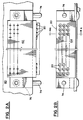
- Fig. 2a is a top view of the connector invention showing a row of contact elements with second ends extending appropriately out of the housing.
- Fig. 2b is a front view of the connector invention.
- Fig. 3a is a cross sectional view of the connector through line A-A of Figure 2b.
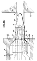
- Fig. 3b is an enlarged cross sectional view of the self-centering tapered funnel of the housing shown in Fig. 3a with a contact element located therein in an unengaged extended position, and in engaged depressed positions.
- Fig. 3c is a partially cut-away top view of the connector taken along line C-C of Figure 3a.
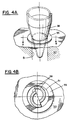
- Fig. 4a is a perspective enlarged view of the tapered end of a single preferred split-cone contact element in contact with a preferred embodiment of the mother card plated through hole.
- Fig. 4b is a cross sectional view of the tapered end of a single preferred split-cone contact element of the connector through line B-B of Fig. 4a.
- Fig. 4c is a force diagram for a typical contact element of the connector, showing both axial insertion (hold-in) and mating contact normal forces.
- Fig. 4d is a cross sectional view of an embodiment of the invention where two connectors are connected to a mid-plane.
- Figs. 5a1 - 5a3, 5b1 - 5b3, 5c1 - 5c3, and 5d1 - 5d3 show alternative embodiments of the tapered end of the contact element, and vertical and horizontal cross-sections therethrough.
- Fig. 6a is a side view of a contact element of the invention prior to its formation into a spring contact.
- Fig. 6b is partial cross sectional view of the connector of the invention where the contact element of Fig. 6a is shown in the process of being formed into a preloaded spring contact through the use of a tool and the housing.
- Figs. 7a and 7b are partially cut-away side views of the alternative connector of the selective contact actuation or ZIF embodiment of the invention.
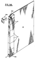
- Fig. 8a is a perspective view of a spring loaded jack screw for use in conjunction with a plurality of connectors so as to maintain the connectors in contact with the mother board.
- Fig. 8b is a side view of an alternative embodiment of a part of the spring loaded jack screw of Fig. 6a.
- Fig. 9a is a perspective view of a first magnet system for use in conjunction with a plurality of connectors so as to maintain the connectors in contact with the mother board.
- Fig. 9b is a perspective view of a second magnet system for use in conjunction with a plurality of connectors so as to maintain the connectors in contact with the mother board.
- Figs. 10 ⁇ a and 10 ⁇ b are respectively a partially cut-away perspective view and enlarged cross-sectional view of a first alternate embodiment of the mother board of the invention which incorporates an alignment grid which permits increased alignment tolerance for the connector invention.
- Fig. 11 is an enlarged cross-section of a second alternate embodiment of the mother board which includes a special compliant layer over a standard PCB board for enhancing contact performance.
- Figures 1, 2a, 2b, 3a - 3c, and 4a - 4c show a first preferred connector assembly of the invention.
- the connector assembly 10 ⁇ typically comprises a plurality of contact elements 20 ⁇ , and a dielectric housing 30 ⁇ for housing the contact elements.
- the contact elements 30 ⁇ are spring pins with first ends 32, second ends 34, and a middle bend section 36.
- the first ends 32 of pins 20 ⁇ extend through holes 39 in the daughter board 40 ⁇ and are preferably soldered to the back side 41 of the daughter board. At least a portion of the first ends 32 is preferably v-shaped to help align the first ends in the holes 39 of the daughter board 40 ⁇ .
- the shape of first ends 32 also provides stiffness, and helps in preloading the contacts as will be discussed hereinafter.
- the second ends 34 of the contact elements 30 ⁇ are basically comprised of a neck portion 35 which may be channel shaped for stiffness, and a tapered contact portion 38. As seen in Fig. 3b, connecting the neck portion 35 to the contact portion 38 is an angled portion 37 which acts in conjunction with the housing to provide self-alignment and preloading as will be described hereinafter.
- the mid-sections 36 of pins 20 ⁇ are preferably crimped to cause pins 20 ⁇ to form a spring.
- pins 20 ⁇ are preferably crimped to first form a one hundred eighty degree bend and then a minus ninety degree bend, and are thus essentially bent through ninety degrees. If desired, a simple bend of ninety degrees could be used, provided mid-sections 36 form spring elements.
- the mid-sections 36 resiliently deflect away from the mother board 50 ⁇ ; i.e. the mid-sections 36 are compliant along the mating axis. In so doing, the mid-sections 36 provide pins 30 ⁇ with a mating force.
- the contact portions 38 of the second ends 34 of contact elements 20 ⁇ are tapered in cross section, with the cross section becoming larger further away from the end or tip of the contact element.
- the contact portions 38 are used to make contact with the plated through holes 51 of the mother board 50 ⁇ .
- the contact portions 38 of the second ends 34 are the preferred split (bifurcated) cones (as seen in Figs. 4a and 4b)
- contact is made between the connector 10 ⁇ and the mother board 50 ⁇ at two points 53a, 53b (radius contact "points") for each contact element 20 ⁇ and through hole 51.
- the contact is made between the tapered portion (i.e. the contact portion 38) of the contact element 20 ⁇ and the rim of hole 51; i.e.
- contact portion 38 In making contact, because contact portion 38 is bifurcated, it resiliently compresses as it is pushed into hole 51, and therefore extends into hole 51 further than it might have otherwise. As a result, the surface of contact portion 38 wipes along the rim of hole 51 as it makes contact providing desired "wipe" and enhanced contact.
- the mother board 50 ⁇ provides a normal contact force F N /2 (shown as the hypotenuse of the triangle).
- Each normal contact force is the result of two perpendicular forces; an axial force of twenty-five grams opposite to the mating force (as required to provide an equal but opposite force to the axial mating force); and a force perpendicular to the axial force.
- the perpendicular forces to the axial forces are equal and opposite each other and therefore cancel.
- the tapered contact portion 38 of pin 20 ⁇ may take any of numerous embodiments.
- the most conventional candidates would be a sphere, a cone, a four edged pyramid, and a three edged pyramid or tetrahedron.
- each such contact portion is tapered and would therefore contact the hole.
- the contact, as seen in Figs. 5a3 - 5d3, might range from a three point contact for the tetrahedron, to irregular annular contact for the sphere and cone.
- the compliant bifurcated cone of Fig. 4a and 4b is the preferred embodiment, followed by the tetrahedron.
- the housing 30 ⁇ includes side walls 60 ⁇ which separate and electrically insulate each column of contact pins 20 ⁇ ; the side walls 60 ⁇ extending perpendicularly from top wall 62. Also extending perpendicularly from top wall 62 is front wall 64 having a plurality of openings 66 for permitting at least a portion of tapered contact portions 38 (and preferably the entire tapered contact portion) of contact pins 20 ⁇ to extend therethrough. Openings 66 are preferably tapered funnels which are arranged to interact with the angled portion 37 of the second ends 34 of the contact pins as will be hereinafter described.
- each guide wall extends slightly past the middle bent portion 36 of the pin contact below it, but only as far as the second end 34 of the pin above it.
- Fig. 3b explores the axial and lateral tolerances built into the connector contact pins relative to the plated through holes of the mother board.
- angled portions 37 contact the funnel-like openings 66 and thereby center themselves therein in a nominal position.
- the openings 66 act as a stop to the contact spring pins 20 ⁇ to cause the spring pins to be preloaded in the housing, as will be discussed hereinafter.
- the contact portions 38 of the pins 20 ⁇ extend out of the housing 30 ⁇ by a desired amount.
- the pins 20 ⁇ When the contact pins 20 ⁇ engage the mother board holes, the pins 20 ⁇ are pushed backward (as seen in phantom) such that the angled portion 37 of the second ends 34 of the pins no longer contacts the funnel-like openings 66 of the housing 30 ⁇ .
- lateral movement of the second end of the pin is expedited in all directions, as the passage for the second end of the pin defined by adjacent side walls 60 ⁇ and adjacent guide walls 68 of the housing 30 ⁇ is wider than the second ends 34 of the pins.
- the further pins 20 ⁇ are pushed backward, the more second ends 34 can move laterally in any direction in the housing passage.
- a tolerance zone or range for the misalignment of a pin relative to a hole is provided which can approach the radius of the hole in size (provided the housing passage and funnel-like opening are large enough).
- the tapering of the contact portion 38 of pin 20 ⁇ provides tolerance relative to the hole diameter, as contact along the tapered surface of the contact portion 38 is guaranteed.
- side walls 60 ⁇ of housing 30 ⁇ preferably include side-wall locking tabs 72 (preferably two per contact) which hold adjacent rows of contacts in a preloaded manner at different fixing points relative to the daughter board 40 ⁇ but at identical fixing points relative to the ninety-degree bend portion 36 of the contact elements 20 ⁇ .
- the locking tabs 72 provide a restriction between adjacent side walls 60 ⁇ through which the v-shaped first end 32 of pins 20 ⁇ are forced during assembly. After the v-shaped first end 32 deforms and passes through the tabs 72, they cannot return past the tabs 72.
- locking tabs 72 act to provide a preload to the spring contact elements 20 ⁇ as the spring contact elements 20 ⁇ are fixed in location on one end by the contact of angled portion 37 with the funnel-like opening 66, and on the other end by locking tabs.
- the locking tabs 72 also act to establish a fixing point which fixes a portion of first end 32 (the portion between the locking tab 72 and the daughter board) against movement in the axis of insertion.
- the tabs 72 act as a strain relief for the first end 32 - daughter board solder joint, as the first end 32 will not substantially move below tab 72.
- the v-shape of first end 32 also helps to stiffen first end 32 and to prevent movement at the solder joint.
- Housing 30 ⁇ may also include at least one integral guide pin 74.
- Guide pin 74 may act as a ground pin by having a ground wire (not shown) wrapped around it, and/or a make first pin for the connector.
- two guide pins 74 are located on either end of the connector and extend along the same axis as the second portion of pins 20 ⁇ .
- the guide pins extend out further than the contact portions 38 of pins 20 ⁇ and thus act in a shielding or protective capacity.
- the guide pins 74 are preferably arranged such that they extend into mating holes in the mother board, with the diameter of the mating holes being as large as or slightly greater than the diameter of non-tapered section of the guide pin.
- first and second guide pins may be oval in cross-section and oriented perpendicularly with respect to one another. In this manner, one guide pin acts as a horizontal guide, while the other acts as a vertical guide.
- the guide pin arrangement is preferably altered.
- a first connector 10 ⁇ a with spring contact elements 20 ⁇ a, and a second connector 10 ⁇ b with spring contact elements 20 ⁇ b are mating with the midplane 50 ⁇ a via plated through holes.
- Midplane 50 ⁇ a includes a guide hole 137 which is slightly larger in diameter than typical guide holes, and connector 10 ⁇ a includes a hollowed guide pin 74a which mates with guide hole 137.
- Connector 10 ⁇ b is a connector according to the teachings of the invention with a standard guide pin 74b which mates with hollowed guide pin 74a.
- the manufacture of the spring contacts for the preferred connector of the invention can be completed, and the spring contacts can be preloaded during the assembly of the connector.
- the contact element 20 ⁇ of the invention is seen in Fig. 6a prior to its insertion into the housing 30 ⁇ .
- Contact element 20 ⁇ includes contact portion 38, angled portion 37, second end 34, middle portion 36, and first end 32. As shown, part of first end 32 is v or u shaped, and part of second end 34 is ribbed or channel shaped. Middle portion 36 is provided with a "dog's-leg" bend.
- manufacture/assembly the contact element 20 ⁇ of Fig.
- first end 32 can only spring back to the vertical position of Fig. 6b because it is restrained by locking tabs 72.
- contact elements 30 ⁇ are preloaded.
- the first end 32 of contact element 20 ⁇ does not spring back to its original shape of Fig. 6a when locking tabs 72 are not present, but rather assumes the position of the spring contact elements of Fig. 1a, the process of bending the contact element 20 ⁇ is seen to form the contacts into spring contacts.
- a connector whose preloaded spring contacts are actually partially manufactured during assembly is provided.
- contact elements 20 ⁇ are preloaded spring contacts, with locking tabs 72 acting as fixing points, if the contact portions 28 of the spring contacts 20 ⁇ are withdrawn into the housing 30 ⁇ , the resulting connector functions as a ZIF connector; i.e. the connector housing can be brought into contact with the mother board with the use of nominal force.
- Two embodiments for retracting contact portions 28 are shown in Figs. 7a and 7b.
- retracting cams 180 ⁇ are provided and can be fixed to side walls 60 ⁇ . By rotating the cams as indicated, the middle portion 26 of the spring contacts 20 ⁇ is forced backward (as shown in phantom), thereby drawing contact portions 28 back towards or into housing 30 ⁇ .
- cams 180 ⁇ may be further rotated to release spring contact 20 ⁇ and permit mating. It will be appreciated that if a single cam is provided for each row of contacts, the rows may be selectively activated. If a cam is provided for each contact, each contact may be selectively activated. Similarly, in Fig. 7b, non-conductive retracting bars 185 which can move along the axis of the second portion 34 of spring contacts 20 ⁇ are provided to force middle portion 26, and hence contact portion 28, backward and provide a ZIF connector. If retracting bars 185 may also be perpendicularly retracted, sequential individual activation of contacts in a single row may be accomplished.
- Figs. 8a, 8b, 9a and 9b various means for establishing and maintaining force on the contact elements when they engage the holes in the mother board are provided.
- the daughter board is provided with a front panel 80 ⁇ , and a stiffening bar 82, with the stiffening bar preferably fastened to the connector housing 30 ⁇ or bearing against the connector housing at the back face (the face opposite front wall 64) thereof.
- a leaf spring 84 with ends abutting the stiffening bar 82 and a middle which bows away from the leaf spring in a direction away from the connectors.
- the stiffening bar, and the leaf spring 84 are holes 86, 88, and 89 for accepting a rod or shaft 90 ⁇ which extends past therethrough.
- a thumbscrew 92 or the like On one end of rod 90 ⁇ is a thumbscrew 92 or the like with an enlarged head which permits turning of the rod.
- Retaining rings 93 and 94 (which is shown in phantom) are also attached to rod 90 ⁇ , with the rings 93 and 94 located on the non-adjacent faces of stiffening bar 82 and leaf spring 84 respectively.
- the second end of rod 90 ⁇ is threaded and terminates in a shoulder.
- the threaded section of rod 90 ⁇ extends past the front face 64 of connectors 10 ⁇ , through a hole in mother board (back plane) 50 ⁇ and is arranged to engage a tapped bushing 95 located on a stiffening channel 97 which runs along the mother board 50 ⁇ , Stiffening channel 97 serves to stiffen the mother board 50 ⁇ so as to prevent bowing of the same due to the large forces exerted by the leaf spring in keeping connectors 10 ⁇ mated in the through holes of the mother board 50 ⁇ .
- a standard spring 84b is used between the stiffening bar 82a and retaining ring 94b. In essence, the system works in an identical manner to that of Fig. 8b.
- FIGs. 9a and 9b Other means of establishing and maintaining force on the connectors are shown in Figs. 9a and 9b.
- simple bar magnets 98a are attached to the daughter PCB 40 ⁇ , with one magnet on either side of the connectors 10 ⁇ .
- Identical poles of each magnet are arranged to face the mother board (not shown) which is provided with one or more steel plates 99a as an attracting surface.
- horseshoe magnets 98b are located alongside each connector 10 ⁇ .
- a steel strip 99b is provided on the mother board to provide an attracting surface for the magnets.
- Figs. 10 ⁇ a, 10 ⁇ b, and 11 changes to the mother board are shown for enhancing the invention.
- grid elements are provided on the surface 55 of the mother board 50 ⁇ around each hole 51.
- the grid elements 10 ⁇ 5 are shaped so as guide the contact portion 38 of the contact elements 20 ⁇ towards hole 51 without stubbing contact portion 38.
- the preferred grid structure shape is substantially parabolic. However, many other shapes can be utilized.
- Grid elements 10 ⁇ 5 provide the connector invention with additional misalignment tolerance relative to the mother board which is particularly useful where relatively large spacing is used between mother board holes. Without the grid elements, the maximum misalignment tolerance of the spring elements 20 ⁇ of connector 10 ⁇ with a hole 51 is the radius of the hole. With grid elements 10 ⁇ 5, the maximum alignment tolerance of the pins to the holes is significantly increased to one half the distance between the holes 51. Such an alignment tolerance is very large compared to other connectors of the art.
- an additional compliant layer 110 ⁇ is shown as an integral part of a specially laminated mother board 50 ⁇ .
- Compliant layer 110 ⁇ is preferably laminated to a conventional FR-4 printed circuit board and provides an appropriate matching compliance for the contact elements 20 ⁇ .
- through hole 51 of the mother board 50 ⁇ is provided with standard copper plating 112.
- gold over nickel (although other contact-quality platings could be used) plating layer 114 is provided atop the copper plating 112 and serves to provide the mating contact surface for the spring contacts 20 ⁇ .
- the compliant layer 110 ⁇ can be provided in situations where additional wipe is required, and/or where frequent insertion of daughter cards is expected.
- the housing and second ends of the spring elements were respectively described as having funnel-like openings in a front wall, and angled portions of the spring element second portions which cooperate with each other, it will be appreciated that geometries other than that shown could be utilized.
- the funnel need not be conical (i.e. the term "funnel-like" being used in its broad sense to suggest a narrow opening and widening out to a large open mouth), while the angled portion need not be straight, providing it does converge.
- the angled portion of the second end need not be circular in cross section, as fins could be utilized for centering purposes.
Landscapes
- Coupling Device And Connection With Printed Circuit (AREA)
- Multi-Conductor Connections (AREA)
Claims (33)
- Elektrischer Steckverbinder zum Bereitstellen einer rechtwinkligen Verbindung zwischen einer Tochter-Leiterplatte (40) und den durchkontaktierten Bohrungen (51) einer Basis-Leiterplatte (50), umfassend:a) mehrere Federkontaktelemente (20), wobei jedes Federkontaktelement einen ersten Teil (32) zum elektrischen Kontaktieren der Tochter-Leiterplatte (40), einen um einen Winkel von ungefähr neunzig Grad gebogenen mittleren Teil (36) und einen zweiten Teil (34), der einen spitz zulaufenden Kontaktteil (38) enthält, aufweist, wobei die Querschnittsfläche des spitz zulaufenden Kontaktteils (38) mit zunehmender Entfernung vom mittleren Teil (36) abnimmt, wobei der spitz zulaufende Teil mit einem Rand einer durchkontaktierten Bohrung (51) der Basis-Leiterplatte (50) zusammenpaßt; undb) ein dielektrisches Gehäuse (30) zum Aufnehmen der mehreren Federkontaktelemente (20) derart, daß die mehreren Federkontaktelemente (20) voneinander elektrisch isoliert sind, wobei der mittlere Teil (36) jedes der Federkontaktelemente (20) nachgiebig ist, um Bewegung des mittleren Teils (36) im wesentlichen entlang einer Achse, die senkrecht zu einer von der Basis-Leiterplatte (50) festgelegten Ebene verläuft, zu gestatten, wenn der spitz zulaufende Kontaktteil (38) des Federkontaktelements (20) die durchkontaktierte Bohrung (51) der Basis-Leiterplatte (50) in Eingriff nimmt.
- Elektrischer Steckverbinder nach Anspruch 1, bei dem das dielektrische Gehäuse (30) eine Vorderwand (64), die parallel zu und neben der Basis-Leiterplatte (50) verläuft, wenn der elektrische Verbinder mit der Basis-Leiterplatte zusammengesteckt wird, wobei die Vorderwand (64) mehrere Öffnungen (66) aufweist, die gestatten, daß mindestens ein Teil des spitz zulaufenden Kontaktteils (38) der Federkontaktelemente (20) sich dort hindurch erstreckt, und mehrere senkrecht zur Vorderwand (64) verlaufende Seitenwände (60) zum elektrischen Trennen von Säulen der mehreren Federkontaktelemente (20) umfaßt.
- Elektrischer Steckverbinder nach Anspruch 2, bei dem das dielektrische Gehäuse (30) mehrere Führungswände (68) umfaßt, wobei jede Führungswand senkrecht zur Vorderwand (64) und den Seitenwänden (60) und im wesentlichen parallel und neben dem zweiten Teil (34) eines der Federkontaktelemente (20) verläuft, wobei die Führungswände (68) Reihen der mehreren Federkontaktelemente (20) elektrisch trennen, wobei mindestens eine Führungswand (68) neben einem Federkontaktelement (20) sich von der Vorderwand (64) aus zum, aber nicht über den mittleren Teil (36) des Federkontaktelements (20) hinaus erstreckt.
- Elektrischer Steckverbinder nach Anspruch 2 oder 3, bei dem die Öffnungen (66) in der Vorderwand (64) des dielektrischen Gehäuses (30) eine im wesentlichen trichterähnliche Form aufweisen und der zweite Teil (34) des Federkontaktelements (20) einen konvergierenden Teil (37) zum Kontaktieren der trichterähnlichen Öffnung zum Anhalten des Federkontaktelements (20) an einer gewünschten Stelle umfaßt.
- Elektrischer Steckverbinder nach Anspruch 4, bei dem die trichterähnliche Öffnung (66) der Vorderwand (64) des dielektrischen Gehäuses (30) und der konvergierende Teil (37) des zweiten Teils (34) des Federkontaktelements (20) so angeordnet sind, daß sie bewirken, daß das Federkontaktelement (20) vorgespannt ist.
- Elektrischer Steckverbinder nach Anspruch 5, bei dem die Führungswände (68) und die Seitenwände (60) Durchgänge für die Federkontaktelemente (20) bilden, wobei jeder Durchgang im Querschnitt größer ist als der größte Querschnitt des im Durchgang befindlichen konvergierenden Teils (37) des Kontaktelements (20).
- Elektrischer Steckverbinder nach einem der Ansprüche 2 bis 6, bei dem die mehreren Seitenwände (60) Rastnasen (72) zum Halten der ersten Teile (32) der Federkontaktelemente (20) an Fixierpunkten aufweisen, die bewirken, daß die Federkontaktelemente (20) vorgespannt sind.
- Elektrischer Steckverbinder nach Anspruch 7, bei dem die ersten Teile (32) der Federkontaktelemente (20) mindestens einen Teil aufweisen, der im wesentlichen V-förmig ist, wobei der V-förmige Teil zwar im wesentlichen nachgiebig ist, so daß der V-förmige Teil von den Rastnasen (72) in eine erste Richtung gedrängt werden kann, aber doch starr genug, um sich einer Bewegung des V-förmigen Teils in einer der ersten Richtung entgegengesetzten zweiten Richtung an den Rastnasen (72) vorbei zu widersetzen.
- Elektrischer Steckverbinder nach Anspruch 7 oder 8, bei dem die Rastnasen (72) an den Seitenwänden (60) des dielektrischen Gehäuses (30) derart angeordnet sind, daß sie die ersten Teile (32) der Federkontaktelemente (20) bezüglich der Tochter-Leiterplatte (40) an unterschiedlichen Fixierpunkten, jedoch bezüglich der mittleren Teile (36) der Federkontaktelemente (20) an identischen Fixierpunkten halten.
- Elektrischer Steckverbinder nach einem vorausgehenden Anspruch, der weiterhin einen einstückig ausgebildeten Führungsstift (74) zum Zusammenstecken mit einer Führungsbohrung der Basis-Leiterplatte (50) umfaßt, wobei sich der Führungsstift (74) entlang einer parallel zu den Längsachsen der Federkontaktelemente (20) verlaufenden Achse erstreckt, wobei sich der einstückig ausgebildete Führungsstift (74) weiter als die Federkontaktelemente (20) nach außen erstreckt und mit der Führungsbohrung der Basis-Leiterplatte (50) zusammengesteckt wird, ehe die mehreren Federkontaktelemente (20) mit den Bohrungen (51) in der Basis-Leiterplatte (50) zusammengesteckt werden, und der einstückig ausgebildete Führungsstift (74) elektrisch angeschlossen ist.
- Elektrischer Steckverbinder nach einem vorausgehenden Anspruch, der weiterhin Herauszugsmittel (180) umfaßt, um mindestens einen der mittleren Teile (36) der Federkontaktelemente (20) in Eingriff zu nehmen und den mindestens einen mittleren Teil (36) lösbar in einer Position zu halten, wo der spitz zulaufende Kontaktteil (38) in Richtung des dielektrischen Gehäuses (30) zurückgezogen wird.
- Elektrischer Steckverbinder nach Anspruch 11, bei dem für jede Reihe der Federkontaktelemente (20) mindestens ein Herauszugsmittel (180) bereitgestellt ist; und das Herauszugsmittel entweder ein Nockenmittel oder eine Stange (185), das bzw. die von mindestens einer der Seitenwände (60) abgestützt ist, umfaßt.
- Elektrischer Steckverbinder nach Anspruch 4 oder 5 im Zusammenhang mit der Basis-Leiterplatte (50), bei dem die Basis-Leiterplatte (50) ein Ausrichtungs-Gittermittel (105) umfaßt, um einen Kontaktteil (38) des zweiten Teils (34) eines Federkontaktelements (20) in eine Durchgangsbohrung (51) hineinzuführen, ohne den Kontaktteil (38) an der Basis-Leiterplatte (50) herauszureißen, wobei das Ausrichtungsgitter (105) zusammen mit der trichterähnlichen Öffnung (66) und dem konvergierenden Teil (37) des zweiten Teils (34) des Federkontaktelements (20) das Federkontaktelement (20) mit einer Ausrichtungstoleranz versieht, die größer ist als der Radius der Durchgangsbohrung (51).
- Elektrischer Steckverbinder nach einem vorausgehenden Anspruch zusammen mit einem Befestigungsmittel, wobei das Befestigungsmittel Mittel zum Aufrechterhalten von Kraft auf dem elektrischen Steckverbinder umfaßt, um die mehreren Federkontaktelemente (20) im Eingriff in den durchkontaktierten Bohrungen (51) der Basis-Leiterplatte (50) zu halten; wobei das Befestigungsmittel ein erstes Mittel, das an eine Rückseite des elektrischen Verbinders anstößt, ein zweites Mittel, das an der Basis-Leiterplatte angebracht ist, und ein Befestigungsmittel umfaßt, das das erste und das zweite Mittel in Eingriff nimmt, um das erste und das zweite Mittel aufeinanderzu zu ziehen; und wobei das erste Mittel eine Verstärkungsstange (82) mit einem ersten Loch darin umfaßt; wobei das zweite Mittel eine mit Innengewinde versehene Durchführung (95) umfaßt; und wobei das Befestigungsmittel einen mit einem Gewinde versehenen Stab (90), der mit der mit Innengewinde versehenen Durchführung (95) zusammenpaßt, und ein an dem mit Gewinde versehenen Stab angebrachtes Arretiermittel, das verhindert, daß der Stab durch die erste Bohrung der Verstärkungsstange zurückgezogen wird, umfaßt.
- Elektrischer Steckverbinder nach einem der vorhergehenden Ansprüche zusammen mit einem Befestigungsmittel nach Anspruch 14, bei dem das zweite Mittel weiterhin einen Verstärkungskanal (97), der die mit Innengewinde versehene Durchführung enthält, umfaßt; und wobei das Befestigungsmittel weiterhin Federmittel (84b) und ein zweites Arretiermittel umfaßt, wobei das Federmittel die Verstärkungsstange (82) auf derjenigen Seite der Verstärkungsstange in Eingriff nimmt, die der Seite der Verstärkungsstange gegenüberliegt, die an die Verbinder (20) stößt, wobei das zweite Arretiermittel an dem mit Gewinde versehenen Stab (90) angebracht ist, um das Federmittel in einer zusammengedrückten Position zu halten.
- Elektrischer Steckverbinder zum Bereitstellen einer elektrischen Verbindung zwischen einer ersten Leiterplatte (40) und durchkontaktierten Bohrungen (51) einer zweiten Leiterplatte (50), umfassend:a) mehrere Federkontaktelementmittel (20), wobei jedes Federkontaktelementmittel (20) einen ersten Teil (32) zum elektrischen Kontaktieren der ersten Leiterplatte (40) und einen zweiten Teil (34), der einen spitz zulaufenden Kontaktteil (38) zum Zusammenstecken mit einem Rand einer durchkontaktierten Bohrung (51) der zweiten Leiterplatte (50) enthält, aufweist, wobei das Federkontaktelementmittel (20) seitlich Toleranz hat, so daß der spitz zulaufende Kontaktteil (38) sich seitlich auf im wesentlichen frei treibende Weise bewegen kann, so daß er im Rand der durchkontaktierten Bohrung (51) der zweiten Leiterplatte (50) positioniert wird; undb) ein dielektrisches Gehäuse (30) zum Aufnehmen der mehreren Federkontaktelemente (20), bei dem mindestens zwei der Federkontaktelementmittel (20) voneinander elektrisch isoliert sind,wobei die zum Zusammenstecken der mehreren Federkontaktelementmittel (20) mit den Rändern der durchkontaktierten Bohrungen (51) erforderliche axiale Steckkraft zu den normalen Kontaktkräften in Beziehung steht, die erzeugt werden, wenn die mehreren Federkontaktelementmittel (20) mit den Rändern der durchkontaktierten Bohrungen (51) zusammengesteckt werden, und wobei die normale Kontaktkraft größer ist als die Steckkraft.
- Elektrischer Steckverbinder nach Anspruch 16, bei dem die normale Kontaktkraft mit der Steckkraft im wesentlichen gemäß der Beziehung FN = FA/sin θ in Beziehung steht, wobei FN die normale Kontaktkraft ist, FA die Steckkraft ist und θ der Konuswinkel des spitz zulaufenden Teils (38) des Federkontaktelementmittels (20) ist.
- Elektrischer Steckverbinder nach Anspruch 16 oder 17, bei dem das dielektrische Gehäuse (30) eine Vorderwand (64), die parallel zu und neben der zweiten Platte (50) verläuft, wenn der elektrische Verbinder mit der zweiten Platte (50) zusammengesteckt wird, wobei die Vorderwand (64) mehrere Öffnungen (66) aufweist, die gestatten, daß mindestens ein Teil des spitz zulaufenden Kontaktteils (38) der Federkontaktelemente (20) sich dort hindurch erstreckt, mehrere senkrecht zur Vorderwand (64) verlaufende Seitenwände (60) zum elektrischen Trennen von Säulen der mehreren Federkontaktelementmittel (20) und mehrere Führungswände (68) umfaßt, wobei jede Führungswand senkrecht zur Vorderwand (64) und den Seitenwänden (60) und im wesentlichen parallel und neben dem zweiten Teil (34) des einen der Federkontaktelementmittel (20) verläuft, wobei die Führungswände (68) Reihen der mehreren Federkontaktelementmittel (20) elektrisch trennen.
- Elektrischer Steckverbinder nach Anspruch 18, bei dem der zweite Teil (34) des Federkontaktelementmittels (20) einen geformten Teil (37) enthält und die Öffnungen (66) in der Vorderwand (64) so geformt sind, daß sie bewirken, daß der geformte Teil (37) die Öffnung (66) kontaktiert, um das Federkontaktelementmittel (20) in einer gewünschten Stelle derart anzuhalten, daß die Federkontaktelementmittel (20) vorgespannt sind.
- Elektrischer Steckverbinder nach Anspruch 18 oder 19, bei dem die Führungswände (68) und die Seitenwände (60) Durchgänge für die Federkontaktmittel (20) bilden, wobei jeder Durchgang so angeordnet ist, daß ein darin befindliches Federkontaktelementmittel (20) sich seitlich bewegen kann, wenn das Federkontaktelementmittel (20) den Rand kontaktiert.
- Elektrischer Steckverbinder nach einem der Ansprüche 16 bis 20, wobei die mehreren Federkontaktelementmittel (20) in mindestens zwei Reihen angeordnet sind, und weiterhin mit Rastmitteln (72) zum Halten der ersten Teile der Federkontaktelementmittel (20) einer ersten Reihe an anderen Fixierpunkten als die Federkontaktelementmittel einer zweiten Reihe derart, daß die Federkontaktelementmittel der ersten Reihe und der zweiten Reihe im wesentlichen identische Federparameter aufweisen.
- Elektrischer Steckverbinder nach einem vorausgehenden Anspruch, wobei der spitz zulaufende Kontaktteil (38) des Kontaktelements (20) einen nachgiebigen, geschlitzten Kegel umfaßt.
- Elektrischer Steckverbinder nach einem der Ansprüche 16 bis 21, der weiterhin Herauszugsmittel (180) umfaßt, um die Federkontaktelementmittel (20) in Eingriff zu nehmen und um die Federkontaktelementmittel (20) lösbar in einer Position zu halten, wo der spitz zulaufende Kontaktteil (38) in Richtung des dielektrischen Gehäuses (30) zurückgezogen wird.
- Elektrischer Steckverbinder nach einem der Ansprüche 16 bis 21 und 23 zusammen mit der zweiten Leiterplatte (50), bei dem die zweite Leiterplatte (50) ein Ausrichtungs-Gittermittel (105) zum Führen eines Kontaktteils (38) des zweiten Teils (34) eines Federkontaktelementmittels (20) in eine Durchgangsbohrung (51) hinein umfaßt, ohne den Kontaktteil (38) an der zweiten Leiterplatte (50) herauszureißen.
- Elektrischer Steckverbinder nach Anspruch 1, 3 und 16 zusammen mit einem Befestigungsmittel, wobei das Befestigungsmittel Mittel zum Aufrechterhalten von Kraft auf dem elektrischen Steckverbinder umfaßt, um die mehreren Federkontaktelementmittel (20) in den durchkontaktierten Bohrungen (51) der zweiten Leiterplatte (50) in Eingriff zu halten.
- Elektrischer Steckverbinder nach einem vorausgehenden Anspruch zusammen mit einem Befestigungsmittel nach Anspruch 25, wobei das Befestigungsmittel mindestens einen an dem Verbinder oder der ersten Leiterplatte angebrachten Magnet (98a) und ein Mittel, das zu dem an der zweiten Platte angebrachten Magnet hingezogen wird, umfaßt.
- Elektrischer Steckverbinder nach einem vorausgehenden Anspruch zusammen mit einem Befestigungsmittel nach Anspruch 25, wobei das Befestigungsmittel erste Mittel (82), die an den elektrischen Verbinder anstoßen, zweite Mittel, die an der zweiten Leiterplatte angebracht sind, und Befestigungsmittel umfaßt, die die ersten und die zweiten Mittel in Eingriff nehmen, um die ersten und die zweiten Mittel aufeinanderzu zu ziehen.
- Verfahren zum Zusammenbauen eines elektrischen Steckverbinders aus Ausgangsbauteilen einschließlich eines dielektrischen Gehäuses (30) mit einer Vorderwand (64) mit mehreren Öffnungen (66) und mehreren ersten Wänden (60), die mehrere an der Vorderwand endende Durchgänge bilden, und mehreren Kontaktelementen (20) mit einem ersten Teil (32) zum elektrischen Kontaktieren einer Tochter-Leiterplatte (40), einem mittleren Teil (36), der über einen Winkel von ungefähr neunzig Grad gebogen werden kann, um eine Feder zu bilden, und einem zweiten Teil (34) einschließlich eines spitz zulaufenden Kontaktteils (38), wobei das Verfahren folgendes umfaßt:a) Einsetzen der mehreren Kontaktelemente (20) in die mehreren Durchgänge zu gewünschten Stellen derart, daß mindestens ein Teil des spitz zulaufenden Kontaktteils (38) der Kontaktelemente (20) sich durch die Öffnungen (66) erstreckt, und derart, daß die zweiten Teile (32) der Kontaktelemente (20) das dielektrische Gehäuse (30) in Eingriff nehmen;b) Halten der Kontaktelemente (20) bei ungefähr den mittleren Teilen (36) der Kontaktelemente;c) während des Haltens der Kontaktelemente (20), Biegen der Kontaktelemente an den mittleren Teilen (36) um ungefähr neunzig Grad derart, daß die Kontaktelemente zu Federkontaktelementen werden, und derart, daß die ersten Teile (32) der Federkontaktelemente das dielektrische Gehäuse (30) in Eingriff nehmen; undd) Lösen des Halts an ungefähr den mittleren Teilen (36) der Federkontaktelemente (20).
- Verfahren nach Anspruch 28, bei dem der Schritt des Haltens der Kontaktelemente (20) das Einsetzen eines ersten Werkzeugs (140) in das dielektrische Gehäuse (30) umfaßt, wobei das erste Werkzeug die Kontaktelemente (20) an ungefähr den mittleren Teilen (36) der Kontaktelemente hält; und der Schritt des Biegens der Kontaktelemente (20) umfaßt, mindestens die ersten Teile (32) der Kontaktelemente (20) mit einem zweiten Werkzeug in Eingriff zu nehmen und zu bewirken, daß sich das zweite Werkzeug auf eine Art bewegt, daß es die Kontaktelemente so biegt, daß sie zu Federkontaktelementen werden, und dann das zweite Werkzeug herauszuziehen.
- Verfahren nach Anspruch 29, bei dem die Vorderwandöffnungen (66) trichterähnliche Form aufweisen; und der zweite Teil (34) jedes der Kontaktelemente (20) weiterhin einen konvergierenden Teil (37) aufweist, wobei mindestens ein Teil des konvergierenden Teils nicht durch eine trichterähnliche Öffnung hindurchpaßt, so daß in dem Einsetzschritt der Kontakt des konvergierenden Teils (37) mit der trichterähnlichen Öffnung (66) einen Anschlag zum Begrenzen der gewünschten Stelle bildet.
- Verfahren nach Anspruch 30, bei dem das dielektrische Gehäuse (30) mehrere zur Vorderwand (64) senkrechte Seitenwände (60) und mehrere zur Vorderwand und den Seitenwänden senkrechte Führungswände (68) umfaßt, wobei die Seitenwände und die Führungswände Durchgänge bilden, und die Seitenwände (60) weiterhin Rastmittel (72) zum Halten der ersten Teile (32) der Federkontaktelemente an Fixierpunkten umfassen und der Schritt des Biegens der Kontaktelemente (20) das Biegen der Kontaktelemente derart umfaßt, daß die ersten Teile (32) an den Seitenwand-Verriegelungsmitteln (72) vorbeigeschoben und von ihnen in Position verriegelt werden.
- Verfahren nach Anspruch 31, wobei die mehreren ersten Wände (60) mindestens eine erste und eine zweite Reihe von Durchgängen in dem dielektrischen Gehäuse (30) festlegen und das Verfahren weiterhin das Einsetzen, Halten, Biegen und Lösen, wie in Schritten a-d dargelegt, für eine erste Mehrheit von Kontaktelementen in einer ersten Reihe von Durchgängen und dann das Einsetzen, Halten, Biegen und Lösen, wie in Schritten a-d dargelegt, für eine zweite Mehrheit von Kontakten in einer zweiten Reihe von Durchgängen umfaßt.
- Verfahren nach Anspruch 32, bei dem die Rastmittel (72) an den Seitenwänden (60) des dielektrischen Gehäuses (30) so angeordnet sind, daß sie die ersten Teile (32) der Federkontaktelemente (20) zwar bezüglich der Tochter-Leiterplatte (40) an verschiedenen Fixierpunkten, jedoch bezüglich der mittleren Teile der Federkontaktelemente (20) an identischen Fixierpunkten halten.
Applications Claiming Priority (3)
| Application Number | Priority Date | Filing Date | Title |
|---|---|---|---|
| US07/366,546 US4966556A (en) | 1989-06-13 | 1989-06-13 | Electrical connector for direct connection to plated through holes in circuit board |
| US366546 | 1989-06-13 | ||
| PCT/US1990/003298 WO1990016097A1 (en) | 1989-06-13 | 1990-06-11 | Electrical connector for direct connection to plated through holes in circuit board |
Publications (3)
| Publication Number | Publication Date |
|---|---|
| EP0479852A1 EP0479852A1 (de) | 1992-04-15 |
| EP0479852A4 EP0479852A4 (en) | 1993-01-13 |
| EP0479852B1 true EP0479852B1 (de) | 1997-03-12 |
Family
ID=23443479
Family Applications (1)
| Application Number | Title | Priority Date | Filing Date |
|---|---|---|---|
| EP90909875A Expired - Lifetime EP0479852B1 (de) | 1989-06-13 | 1990-06-11 | Elektrischer verbinder zur direkten verbindung von durchkontaktierten bohrungen von leiterplatten |
Country Status (7)
| Country | Link |
|---|---|
| US (1) | US4966556A (de) |
| EP (1) | EP0479852B1 (de) |
| JP (1) | JPH04506279A (de) |
| AU (1) | AU5920590A (de) |
| CA (1) | CA2060313C (de) |
| DE (1) | DE69030183T2 (de) |
| WO (1) | WO1990016097A1 (de) |
Families Citing this family (20)
| Publication number | Priority date | Publication date | Assignee | Title |
|---|---|---|---|---|
| US5366380A (en) * | 1989-06-13 | 1994-11-22 | General Datacomm, Inc. | Spring biased tapered contact elements for electrical connectors and integrated circuit packages |
| US5425649A (en) * | 1989-06-13 | 1995-06-20 | General Datacomm, Inc. | Connector system having switching and testing functions using tapered spring contact elements and actuators therefor |
| US20020004320A1 (en) * | 1995-05-26 | 2002-01-10 | David V. Pedersen | Attaratus for socketably receiving interconnection elements of an electronic component |
| US5597317A (en) * | 1995-08-11 | 1997-01-28 | W. L. Gore & Associates, Inc. | Surface mating electrical connector |
| JP3506202B2 (ja) * | 1997-06-30 | 2004-03-15 | 住友電装株式会社 | 基板用コネクタ |
| US6146924A (en) * | 1999-08-06 | 2000-11-14 | Vanguard International Semiconductor Corporation | Magnetic insert into mold cavity to prevent resin bleeding from bond area of pre-mold (open cavity) plastic chip carrier during molding process |
| US20020076990A1 (en) * | 2000-12-15 | 2002-06-20 | Sumitomo Wiring Systems Ltd. | Apparatus for processing a stacked-type connector of a wire harness, a housing holder, apparatus and method and for stacking housings of a stacked-type connectors, and apparatus for pressing a joint portion of stacked-type connector |
| US7000309B1 (en) * | 2002-06-28 | 2006-02-21 | Western Digital Technologies, Inc. | Method of assembling a disk drive by electrically grounding a disk drive cover |
| JP2005072385A (ja) * | 2003-08-26 | 2005-03-17 | Sumitomo Wiring Syst Ltd | バスバーのタブとプリント基板の半田接続構造 |
| CN2770142Y (zh) * | 2004-12-25 | 2006-04-05 | 富士康(昆山)电脑接插件有限公司 | 背板连接器 |
| US7435109B1 (en) * | 2007-11-26 | 2008-10-14 | Yokowo Co., Ltd. | Spring connector |
| CN101574773B (zh) * | 2008-05-08 | 2010-12-15 | 华通电脑股份有限公司 | 印刷电路板的定位销装配装置 |
| HK1209237A1 (en) | 2012-09-03 | 2016-03-24 | I-Blades, Inc. | Method and system for smart contact arrays and stacked devices |
| US8764458B1 (en) * | 2012-09-10 | 2014-07-01 | Amazon Technologies, Inc. | Spring connector and corresponding guide element |
| US9703321B2 (en) | 2013-07-09 | 2017-07-11 | I-Blades, Inc. | Snap on wearable module |
| GB2527084A (en) * | 2014-06-11 | 2015-12-16 | Ibm | Cable securing apparatus and method of securing a cable |
| US9690056B2 (en) * | 2014-06-25 | 2017-06-27 | Samtec, Inc. | Connector assembly |
| US10279696B2 (en) * | 2015-10-19 | 2019-05-07 | International Business Machines Corporation | Electric vehicle automatic charging station |
| CN106450820B (zh) * | 2016-11-01 | 2019-03-15 | 夏成文 | 一种卡座及与该卡座适配的插座 |
| CN121315614A (zh) * | 2023-10-11 | 2026-01-13 | 江苏神马电力股份有限公司 | 一种自动定位压接系统 |
Family Cites Families (66)
| Publication number | Priority date | Publication date | Assignee | Title |
|---|---|---|---|---|
| US3215968A (en) * | 1960-12-21 | 1965-11-02 | Adolf L Herrmann | Printed circuit board connector |
| US3144527A (en) * | 1961-09-13 | 1964-08-11 | Manuel J Tolegian | Magnetic electrical coupling |
| NL136808C (de) * | 1965-05-07 | |||
| US3407378A (en) * | 1966-05-24 | 1968-10-22 | Hersey Sparling Meter Company | Electrical contact system |
| US3404362A (en) * | 1966-07-29 | 1968-10-01 | Bendix Corp | Selective indexing guide device for electrical connectors of printed circuit cards |
| GB1150233A (en) * | 1966-09-19 | 1969-04-30 | Clarke & Smith Controls Ltd | Improvements in or relating to Electrical Connectintg Devices. |
| US3430182A (en) * | 1967-04-27 | 1969-02-25 | Nasa | Electrical feed-through connection for printed circuit boards and printed cable |
| US3550062A (en) * | 1967-12-26 | 1970-12-22 | Gen Electric | Connector and mounting device for printed wiring boards |
| US3504328A (en) * | 1968-01-03 | 1970-03-31 | Berg Electronics Inc | Circuit board eyelet |
| US3601762A (en) * | 1969-08-15 | 1971-08-24 | Vernitron Corp | Electrical connector |
| US3783433A (en) * | 1971-01-18 | 1974-01-01 | Litton Systems Inc | Solderless electrical connection system |
| US4012093A (en) * | 1971-08-25 | 1977-03-15 | The Deutsch Company Electronic Components Division | Connector arrangement for thin, deflectable conductors |
| US3810258A (en) * | 1972-07-11 | 1974-05-07 | W Mathauser | Quick connect electrical coupler |
| DE2344239B2 (de) * | 1973-09-01 | 1977-11-03 | Luther, Erich, 3050 Wunstorf; Maelzer, Fritz; Maelzer, Martin; 7910 Reutti Post Neu-Ulm; Türkkan, Tamer, 3011 Laatzen | Kontaktvorrichtung zum anschliessen einer gedruckten schaltung an ein pruefgeraet |
| US3885215A (en) * | 1974-01-07 | 1975-05-20 | Unit Process Assemblies | Electrode assembly for measuring the effective thickness of thru-hole plating in circuit board workpieces or the like |
| US4042880A (en) * | 1974-01-07 | 1977-08-16 | Unit Process Assemblies, Inc. | Electrode assembly for measuring the effective thickness of thru-hole plating circuit board workpieces |
| US4004298A (en) * | 1975-03-31 | 1977-01-25 | Sinai Hospital Of Detroit | Magnetically aligned releasable connector |
| US4050769A (en) * | 1976-03-18 | 1977-09-27 | Elfab Corporation | Electrical connector |
| US4164704A (en) * | 1976-11-01 | 1979-08-14 | Metropolitan Circuits, Inc. | Plural probe circuit card fixture using a vacuum collapsed membrane to hold the card against the probes |
| CA1078038A (en) * | 1976-11-22 | 1980-05-20 | Richard C. Holt | Electrical interconnection boards with lead sockets mounted therein and method for making same |
| ZA773036B (en) * | 1977-05-23 | 1978-08-30 | L Mei | Elastomeric electrical contact |
| GB1590458A (en) * | 1977-10-28 | 1981-06-03 | Ferranti Ltd | Electric connectors |
| US4321532A (en) * | 1978-03-16 | 1982-03-23 | Luna L Jack | Repairable spring probe assembly |
| FR2432782A1 (fr) * | 1978-08-02 | 1980-02-29 | Chaillot Gustave | Connecteurs de securite et dispositifs equipes de tels connecteurs |
| US4270826A (en) * | 1979-02-01 | 1981-06-02 | Thomas & Betts Corporation | Zero insertion force connector |
| US4245189A (en) * | 1979-06-14 | 1981-01-13 | Upa Technology, Inc. | Probe assembly for measuring conductivity of plated through holes |
| US4701703A (en) * | 1979-08-13 | 1987-10-20 | Philip M. Hinderstein | Bed-of-pins test fixture |
| US4528500A (en) * | 1980-11-25 | 1985-07-09 | Lightbody James D | Apparatus and method for testing circuit boards |
| US4443756A (en) * | 1980-11-25 | 1984-04-17 | Lightbody James D | Apparatus and method for testing circuit boards |
| US4381134A (en) * | 1981-03-13 | 1983-04-26 | Bell Telephone Laboratories, Incorporated | Electrical connector for plated-through holes |
| FR2507829A1 (fr) * | 1981-06-12 | 1982-12-17 | Cit Alcatel | Connecteur a force d'insertion nulle pour carte de circuit imprime |
| US4448466A (en) * | 1981-11-12 | 1984-05-15 | Ncr Corporation | Low insertion force connector for printed circuit boards |
| US4428640A (en) * | 1981-12-24 | 1984-01-31 | Industrial Electronic Hardware | Protective means for multiple pin connectors |
| US4571542A (en) * | 1982-06-30 | 1986-02-18 | Japan Synthetic Rubber Co., Ltd. | Method and unit for inspecting printed wiring boards |
| US4510553A (en) * | 1983-01-24 | 1985-04-09 | Burroughs Corporation | Electromechanical assembly for aligning, discharging, and sequentially engaging conductors of a P.C. board with a backplane |
| US4548452A (en) * | 1983-06-29 | 1985-10-22 | International Business Machines Corporation | High-density electrical contact pad pattern |
| DE3318135A1 (de) * | 1983-05-18 | 1984-11-22 | Erni Elektroapparate Gmbh, 7321 Adelberg | Loetfreie elektrische verbindung |
| US4479685A (en) * | 1983-06-20 | 1984-10-30 | Exxon Production Research Co. | Flexible magnetic electrical connector and cable incorporating that connector |
| US4541678A (en) * | 1983-07-01 | 1985-09-17 | Trw Inc. | Printed circuit board indexing and locking device |
| US4526429A (en) * | 1983-07-26 | 1985-07-02 | Augat Inc. | Compliant pin for solderless termination to a printed wiring board |
| US4691979A (en) * | 1983-08-04 | 1987-09-08 | Manda R & D | Compliant press-fit electrical contact |
| US4504101A (en) * | 1983-08-29 | 1985-03-12 | Gte Automatic Electric Inc. | Low insertion force connection arrangement |
| US4498722A (en) * | 1983-12-05 | 1985-02-12 | Amp Incorporated | Latch device for ZIF card edge connectors |
| US4533203A (en) * | 1983-12-07 | 1985-08-06 | Amp Incorporated | Connector for printed circuit boards |
| US4606589A (en) * | 1984-01-12 | 1986-08-19 | H & V Services | Compliant pin |
| US4587596A (en) * | 1984-04-09 | 1986-05-06 | Amp Incorporated | High density mother/daughter circuit board connector |
| US4675600A (en) * | 1984-05-17 | 1987-06-23 | Geo International Corporation | Testing apparatus for plated through-holes on printed circuit boards, and probe therefor |
| FR2565737B3 (fr) * | 1984-06-12 | 1986-09-19 | Feinmetall Gmbh | Element de contact pour adaptateur de controle pour effectuer des controles electriques de pieces a controler notamment de circuits imprimes |
| JPS6129080A (ja) * | 1984-07-19 | 1986-02-08 | アルプス電気株式会社 | フイルム被覆端子およびその製造法 |
| EP0177731A3 (de) * | 1984-09-26 | 1987-10-28 | Siemens Aktiengesellschaft | Einschiebbare elektrische Baugruppe |
| DE3441480A1 (de) * | 1984-11-13 | 1986-05-15 | MANIA Elektronik Automatisation Entwicklung und Gerätebau GmbH, 6384 Schmitten | Kontaktstift |
| DE3500227A1 (de) * | 1985-01-05 | 1986-07-10 | Riba-Prüftechnik GmbH, 7801 Schallstadt | Tastnadel |
| US4793817A (en) * | 1985-02-27 | 1988-12-27 | Karl Neumayer, Erzeugung Und Vertreib Von Kabeln, Drahten Isolierten Leitungen Und Elektromaterial Gesellschaft Mit Beschrankter Haftung | Contact pin |
| US4724383A (en) * | 1985-05-03 | 1988-02-09 | Testsystems, Inc. | PC board test fixture |
| FR2585516B1 (fr) * | 1985-07-25 | 1988-03-18 | Legrand Sa | Bloc de jonction a raccordement lateral |
| DE3528912A1 (de) * | 1985-08-12 | 1987-02-19 | Winchester Electronics Divisio | Steckverbinder fuer leiterkarten |
| ATE36197T1 (de) * | 1985-09-16 | 1988-08-15 | Mania Gmbh | Vorrichtung zum elektronischen pruefen von leiterplatten oder dergleichen. |
| US4735587A (en) * | 1986-02-12 | 1988-04-05 | Specialty Electronics, Inc. | Pin header with board retention tail |
| DE8706546U1 (de) * | 1986-05-12 | 1987-09-17 | Feinmetall Gmbh, 7033 Herrenberg | Federkontaktstift |
| US4744764A (en) * | 1986-05-27 | 1988-05-17 | Rogers Corporation | Connector arrangement |
| US4697864A (en) * | 1986-06-19 | 1987-10-06 | Amp Incorporated | Printed circuit board receptacle for sealed connector |
| US4755149A (en) * | 1986-08-15 | 1988-07-05 | Amp Incorporated | Blind mating connector |
| US4795977A (en) * | 1987-03-19 | 1989-01-03 | Pacific Western Systems, Inc. | Interface system for interfacing a device tester to a device under test |
| US4793816A (en) * | 1987-07-20 | 1988-12-27 | Industrial Electronic Hardware | Terminal protector for circuit board connector |
| US4789352A (en) * | 1987-12-02 | 1988-12-06 | Amp Incorporated | Power connector having linearly moving cam for daughter card |
| US4795362A (en) * | 1988-03-03 | 1989-01-03 | Gte Communication Systems, Inc. | Circuit connector for use with printed wiring board |
-
1989
- 1989-06-13 US US07/366,546 patent/US4966556A/en not_active Expired - Lifetime
-
1990
- 1990-06-11 EP EP90909875A patent/EP0479852B1/de not_active Expired - Lifetime
- 1990-06-11 WO PCT/US1990/003298 patent/WO1990016097A1/en not_active Ceased
- 1990-06-11 CA CA002060313A patent/CA2060313C/en not_active Expired - Fee Related
- 1990-06-11 DE DE69030183T patent/DE69030183T2/de not_active Expired - Fee Related
- 1990-06-11 JP JP2509873A patent/JPH04506279A/ja active Pending
- 1990-06-11 AU AU59205/90A patent/AU5920590A/en not_active Abandoned
Also Published As
| Publication number | Publication date |
|---|---|
| CA2060313A1 (en) | 1990-12-14 |
| CA2060313C (en) | 2001-08-14 |
| WO1990016097A1 (en) | 1990-12-27 |
| EP0479852A4 (en) | 1993-01-13 |
| EP0479852A1 (de) | 1992-04-15 |
| DE69030183T2 (de) | 1997-10-09 |
| DE69030183D1 (de) | 1997-04-17 |
| US4966556A (en) | 1990-10-30 |
| JPH04506279A (ja) | 1992-10-29 |
| AU5920590A (en) | 1991-01-08 |
Similar Documents
| Publication | Publication Date | Title |
|---|---|---|
| US4966556A (en) | Electrical connector for direct connection to plated through holes in circuit board | |
| EP0132664B1 (de) | Federnder Stift für Lötfreie Verbindung mit einer gedruckten Schaltung | |
| US5366380A (en) | Spring biased tapered contact elements for electrical connectors and integrated circuit packages | |
| EP0384580B1 (de) | HDI-Kontakt für Oberflächenmontage | |
| CN102640355B (zh) | 具有焊料构件的电触头以及将焊料构件安装到电触头的方法 | |
| JP2996256B2 (ja) | 複数ピン構成要素を回路板へ装着する装置及び方法 | |
| CN1067178C (zh) | 电路板和可边缘装配的连接器及制造电路板边缘的方法 | |
| TWI408848B (zh) | 高效能電連接器 | |
| US5256073A (en) | Electrical connectors for direct connection to plated through holes in circuit board | |
| US11005204B2 (en) | High speed electrical connector assembly | |
| US5482474A (en) | Edge-mountable circuit board connector | |
| WO1996002963A1 (en) | Electrical connector hold-down | |
| EP0331293B1 (de) | Elektrischer Endstückstift mit nachgiebigem Teil | |
| WO1989008339A1 (en) | Tolerance forgiving boardlock | |
| EP0499431B1 (de) | Lanzenförmige Niederhaltevorrichtung | |
| US5009606A (en) | Separable electrical connector | |
| US4718166A (en) | Method of making a connector | |
| EP0546673A2 (de) | Verbinder mit Haltemitteln | |
| EP0305729A2 (de) | Steckverbinder für Leiterplatten | |
| KR101029668B1 (ko) | 표면장착 헤더 조립체 | |
| US5199908A (en) | Electrical contact | |
| EP0364104B1 (de) | Zylindrische Miniaturendkontaktbüchse | |
| US20030190827A1 (en) | Electrical connector having retention contact tails and non-retention contact tails for retaining to a pcb prior to soldering as well as reducing force of inserting the contact tails to the pcb | |
| US6241564B1 (en) | Carrier plate for forming a plug contact | |
| EP0101539A2 (de) | Fingerverbinder für gedruckte Schaltungskarten und Herstellungsverfahren |
Legal Events
| Date | Code | Title | Description |
|---|---|---|---|
| PUAI | Public reference made under article 153(3) epc to a published international application that has entered the european phase |
Free format text: ORIGINAL CODE: 0009012 |
|
| 17P | Request for examination filed |
Effective date: 19911227 |
|
| AK | Designated contracting states |
Kind code of ref document: A1 Designated state(s): DE ES FR GB IT NL SE |
|
| 111Z | Information provided on other rights and legal means of execution |
Free format text: DE ES FR GB IT NL SE |
|
| A4 | Supplementary search report drawn up and despatched |
Effective date: 19921123 |
|
| AK | Designated contracting states |
Kind code of ref document: A4 Designated state(s): DE ES FR GB IT NL SE |
|
| 17Q | First examination report despatched |
Effective date: 19940623 |
|
| GRAG | Despatch of communication of intention to grant |
Free format text: ORIGINAL CODE: EPIDOS AGRA |
|
| GRAH | Despatch of communication of intention to grant a patent |
Free format text: ORIGINAL CODE: EPIDOS IGRA |
|
| GRAH | Despatch of communication of intention to grant a patent |
Free format text: ORIGINAL CODE: EPIDOS IGRA |
|
| GRAA | (expected) grant |
Free format text: ORIGINAL CODE: 0009210 |
|
| AK | Designated contracting states |
Kind code of ref document: B1 Designated state(s): DE ES FR GB IT NL SE |
|
| PG25 | Lapsed in a contracting state [announced via postgrant information from national office to epo] |
Ref country code: IT Free format text: LAPSE BECAUSE OF FAILURE TO SUBMIT A TRANSLATION OF THE DESCRIPTION OR TO PAY THE FEE WITHIN THE PRE;WARNING: LAPSES OF ITALIAN PATENTS WITH EFFECTIVE DATE BEFORE 2007 MAY HAVE OCCURRED AT ANY TIME BEFORE 2007. THE CORRECT EFFECTIVE DATE MAY BE DIFFERENT FROM THE ONE RECORDED.SCRIBED TIME-LIMIT Effective date: 19970312 Ref country code: NL Free format text: LAPSE BECAUSE OF FAILURE TO SUBMIT A TRANSLATION OF THE DESCRIPTION OR TO PAY THE FEE WITHIN THE PRESCRIBED TIME-LIMIT Effective date: 19970312 Ref country code: ES Free format text: THE PATENT HAS BEEN ANNULLED BY A DECISION OF A NATIONAL AUTHORITY Effective date: 19970312 |
|
| REF | Corresponds to: |
Ref document number: 69030183 Country of ref document: DE Date of ref document: 19970417 |
|
| PG25 | Lapsed in a contracting state [announced via postgrant information from national office to epo] |
Ref country code: SE Effective date: 19970612 |
|
| ET | Fr: translation filed | ||
| NLV1 | Nl: lapsed or annulled due to failure to fulfill the requirements of art. 29p and 29m of the patents act | ||
| PLBE | No opposition filed within time limit |
Free format text: ORIGINAL CODE: 0009261 |
|
| STAA | Information on the status of an ep patent application or granted ep patent |
Free format text: STATUS: NO OPPOSITION FILED WITHIN TIME LIMIT |
|
| 26N | No opposition filed | ||
| PGFP | Annual fee paid to national office [announced via postgrant information from national office to epo] |
Ref country code: GB Payment date: 19990609 Year of fee payment: 10 |
|
| PGFP | Annual fee paid to national office [announced via postgrant information from national office to epo] |
Ref country code: FR Payment date: 19990610 Year of fee payment: 10 |
|
| PGFP | Annual fee paid to national office [announced via postgrant information from national office to epo] |
Ref country code: DE Payment date: 19990614 Year of fee payment: 10 |
|
| PG25 | Lapsed in a contracting state [announced via postgrant information from national office to epo] |
Ref country code: GB Free format text: LAPSE BECAUSE OF NON-PAYMENT OF DUE FEES Effective date: 20000611 |
|
| GBPC | Gb: european patent ceased through non-payment of renewal fee |
Effective date: 20000611 |
|
| PG25 | Lapsed in a contracting state [announced via postgrant information from national office to epo] |
Ref country code: FR Free format text: LAPSE BECAUSE OF NON-PAYMENT OF DUE FEES Effective date: 20010228 |
|
| REG | Reference to a national code |
Ref country code: FR Ref legal event code: ST |
|
| PG25 | Lapsed in a contracting state [announced via postgrant information from national office to epo] |
Ref country code: DE Free format text: LAPSE BECAUSE OF NON-PAYMENT OF DUE FEES Effective date: 20010403 |