EP0480182A2 - Circuit pour systèmes optiques anti-bruit - Google Patents
Circuit pour systèmes optiques anti-bruit Download PDFInfo
- Publication number
- EP0480182A2 EP0480182A2 EP91115233A EP91115233A EP0480182A2 EP 0480182 A2 EP0480182 A2 EP 0480182A2 EP 91115233 A EP91115233 A EP 91115233A EP 91115233 A EP91115233 A EP 91115233A EP 0480182 A2 EP0480182 A2 EP 0480182A2
- Authority
- EP
- European Patent Office
- Prior art keywords
- signal
- current
- sample
- component
- steady
- Prior art date
- Legal status (The legal status is an assumption and is not a legal conclusion. Google has not performed a legal analysis and makes no representation as to the accuracy of the status listed.)
- Withdrawn
Links
Images


Classifications
-
- G—PHYSICS
- G01—MEASURING; TESTING
- G01J—MEASUREMENT OF INTENSITY, VELOCITY, SPECTRAL CONTENT, POLARISATION, PHASE OR PULSE CHARACTERISTICS OF INFRARED, VISIBLE OR ULTRAVIOLET LIGHT; COLORIMETRY; RADIATION PYROMETRY
- G01J1/00—Photometry, e.g. photographic exposure meter
- G01J1/10—Photometry, e.g. photographic exposure meter by comparison with reference light or electric value provisionally void
- G01J1/16—Photometry, e.g. photographic exposure meter by comparison with reference light or electric value provisionally void using electric radiation detectors
-
- G—PHYSICS
- G01—MEASURING; TESTING
- G01S—RADIO DIRECTION-FINDING; RADIO NAVIGATION; DETERMINING DISTANCE OR VELOCITY BY USE OF RADIO WAVES; LOCATING OR PRESENCE-DETECTING BY USE OF THE REFLECTION OR RERADIATION OF RADIO WAVES; ANALOGOUS ARRANGEMENTS USING OTHER WAVES
- G01S7/00—Details of systems according to groups G01S13/00, G01S15/00, G01S17/00
- G01S7/48—Details of systems according to groups G01S13/00, G01S15/00, G01S17/00 of systems according to group G01S17/00
- G01S7/491—Details of non-pulse systems
- G01S7/493—Extracting wanted echo signals
-
- H—ELECTRICITY
- H01—ELECTRIC ELEMENTS
- H01S—DEVICES USING THE PROCESS OF LIGHT AMPLIFICATION BY STIMULATED EMISSION OF RADIATION [LASER] TO AMPLIFY OR GENERATE LIGHT; DEVICES USING STIMULATED EMISSION OF ELECTROMAGNETIC RADIATION IN WAVE RANGES OTHER THAN OPTICAL
- H01S3/00—Lasers, i.e. devices using stimulated emission of electromagnetic radiation in the infrared, visible or ultraviolet wave range
- H01S3/10—Controlling the intensity, frequency, phase, polarisation or direction of the emitted radiation, e.g. switching, gating, modulating or demodulating
- H01S3/13—Stabilisation of laser output parameters, e.g. frequency or amplitude
- H01S3/1303—Stabilisation of laser output parameters, e.g. frequency or amplitude by using a passive reference, e.g. absorption cell
Definitions
- the present invention concerns noise cancellation circuitry for use with optical measurement systems.
- the invention relates to a shot-noise limited, all electronic noise cancellation system which is suitable for use with a laser measurement system.
- LIDAR laser-based spectroscopy
- LIDAR light, generated by a laser is detected by electronic apparatus to make a measurement.
- Shot noise is a random current fluctuation that occurs when light is detected.
- Conventional photodetectors such as PIN diodes, pass current from their anode to their cathode in proportion to the number of photons that strike the detector. Each photon can generate only one electron.
- the random current fluctuations occur because the arrival of photons at the photodetector may be accurately modeled as a Poisson process. For any given time interval, there is an average number of photons that are expected to arrive at the detector and a standard deviation representing nominal variations from the average. It is this variation in the arrival of photons, causing a corresponding variation in the current passed by the photodetector, which causes the shot noise.
- the level of noise signals is usually the highest at low modulation frequencies, many high-precision optical measurement systems apply some sort of modulation to the beam. This makes the output signals of the measurement system periodic in time at a frequency that is sufficiently far above the low-frequency noise signals to substantially reduce the effect of the noise on the measurement.
- Another method of reducing noise is to take a sample of the output beam and apply negative feedback to the laser operating current or to an external optical attenuator to keep the photocurrent, derived from the sample beam, constant.
- These systems tend to be complicated or expensive and can, at best, bring the signal-to-noise ratio of the output beam up to the signal-to-shot-noise ratio of the sample beam. Since, in these systems, the sample beam is usually appreciably weaker than the output beam and, so contains relatively more shot-noise, this method may not provide acceptable levels of noise reduction. In addition, since these systems depend on feedback, the effective bandwidth of the noise-reduced beam is often relatively small.
- a laser beam is typically split into a signal beam and a sample beam.
- the signal beam is passed through the optical system to one detector while the sample beam is passed around the optical system to another detector.
- optical systems Due to the wide bandwidth, the optical system does not introduce any differential gain or differential phase to the modulation of the beam as long as the relative path delays between the signal and sample beams are small. In this arrangement, the instantaneous fractional excess amplitude noise of the sample beam is substantially the same as that of the signal beam.
- the linearity of the photodetectors ensures that this is true for the photocurrents as well; thus if the DC components of the two photocurrents cancel, the excess noise components of the photocurrents also cancel at all frequencies of interest.
- the optical system is desirably adjusted so that the photocurrents from the detected signal and sample beams are exactly equal.
- the result of the subtraction operation is a current representing the variations in the signal beam, without the DC component or any of the excess noise signal components of the signal beam.
- Subtracter can be designed to have relatively wide bandwidths since the photocurrents may be subtracted directly without prior conversion to voltages.
- Dividing noise cancellation systems at first may appear to be more desirable than subtractive systems since they do not need precise adjustment and since they cancel fractional rather than absolute noise deviations.
- dividers tend to be relatively slow, limiting the bandwidth of the noise suppressed signal.
- dividing may add significant amounts of noise to the signal.
- U.S. Patent No. 4,896,222 to Fukai relates to a system in which the sample photocurrent is electrically corrected and then subtracted from the signal photocurrent.
- U.S. Patent No. 4,718,121 to Epworth concerns a noise reduction system which uses variable gain amplifiers to reduce laser noise by subtraction.
- This system operates on two beat-frequency signals, one of which is the sum of a signal beam and a local oscillator beam and the other is the difference between these two beams.
- the system measures the noise and adjusts the gains of the two amplifiers to cancel the noise when the signals are summed.
- U.S. Patent No. 4,150,402 to Tietze et al. relates to a system which uses the sample photocurrent as a control signal for a variable gain amplifier which amplifies the signal photocurrent.
- the present invention is embodied in a noise suppression system which balances the photocurrents derived from a signal beam and a sample beam provided by an optical system. With the currents balanced, any residual difference current is a signal representing the information content of the signal beam and is substantially free of any noise components having amplitudes greater than the shot noise in the signal and sample photocurrents.
- the circuitry which balances the two photocurrents includes circuitry configured to subdivide either the signal photocurrent or the sample photocurrent to produce a balanced output photocurrent having the same direct current component as the other one of the signal and sample photocurrents.
- the noise suppression system further includes circuitry which combines the two balanced signals to produce an output signal representing the information components of the signal current, substantially free of noise signal components.
- the circuitry includes a feedback circuit which is responsive to the output signal of the combining circuit for biasing the signal subdividing circuit to maintain the balance between the current signal that it provides and the other photocurrent signal.
- the photocurrents derived from the sample and signal beams are in a ratio of N to 1 where N is greater than 2, and the circuitry further subdivides the photocurrent derived from the sample beam to achieve further shot noise reduction when the balanced sample photocurrent and signal photocurrent are combined.
- a laser 110 is controlled by control circuitry 112 to produce an output beam of light, 111.
- the beam 111 is split by a half-silvered mirror or other suitable beam sampling device 116 into a signal beam 128 and a sample beam 126.
- the signal beam 128 is passed through a gas sample 118, and in so doing, is transformed into a modified signal beam 128'.
- the beam 128' is then reflected from a mirror 120 to reach the signal beam input port of a detector 122.
- the sample beam 126 is reflected from a mirror 124 to reach the sample beam input port of the detector 122.
- a computer 114 sends control signals to the laser controller 112 which may, for example, tune the frequency of the beam provided by the laser 110 through a range of frequencies.
- the computer 114 is also coupled to the detector 122 to capture a linear output signal, LO, provided thereby.
- the computer 114 is optionally coupled to receive a log output signal, LOGO as shown by the phantom connection. This signal is described below in reference to Fig. 3.
- the computer 114 can derive information regarding, for example, the molecular structure of the gas sample 118.
- the beam sampler 116 is configured to pass slightly less than half of the incident beam 111 as the signal beam 128 and to reflect slightly more than half of the beam 111 as the sample beam 126.
- the signal beam is passed with little or no attenuation of its average light intensity through the gas sample 118.
- the sampler 116 should be selected to reflect only enough of the incident beam 111 so that the illumination provided by the sample beam 126 arriving at the detector 122 is somewhat greater than that of the largest steady-state component of the beam 128'.
- An application of this type is one in which the signal beam is reflected off of a target to generate the modified signal beam 128'. For example, if the beam 128 is reflected off of an integrated circuit to expose or to perform measurements on photoresist.
- the signal beam 128' and sample beam 126 are converted into photocurrents.
- the sample beam photocurrent is subdivided, by an electronically controlled pair of transistors, configured as a differential pair, into two currents. One of these currents has substantially the same steady-state current amplitude as the signal photocurrent. This current is subtracted from the signal photocurrent to produce an output signal having only insignificant levels of the direct current (DC) and excess noise components of the signal photocurrent.
- DC direct current
- the adjustment which controls the balancing of the sample and signal photocurrents is controlled by using negative feedback to ensure that the difference of their DC components is zero. This embodiment is described below with reference to Fig. 3.
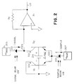
- Fig. 2 is a schematic diagram, partly in block diagram form of exemplary circuitry which may be used as the detector 122, shown in Fig. 1.
- a signal photodiode 210 and a sample photodiode 212 are activated by the respective signal beam 128' and sample beam 126 to pass current provided by sources of operational power 205 and 207, respectively.
- the photocurrent passed by the photodiode 210, less the collector current I C2 of transistor Q2, is applied to the summing junction of a conventional transresistance amplifier A1.
- the amplifier A1 converts the net current at its summing junction to a voltage signal, LO which is the linear output signal of the detector 122.
- the operational potentials provided by the respective sources 205 and 207 depend on the type of photodetectors used.
- the photodetectors 210 and 212 are silicon PIN diodes and the sources 205 and 207 provide +12 volts and -12 volts, respectively.
- the sample photocurrent passed by the photodiode 212 is applied to joined emitter electrodes of a pair of bipolar transistors, Q1 and Q2 which are configured as a differential pair.
- the transistors Q1 and Q2 are fast, matched transistors having current gain - bandwidth products (f T ) of approximately 5 GHz.
- the collector and base electrodes of the transistor Q1 are coupled to a source of reference potential (e.g. ground), the base electrode of transistor Q2 is coupled to a source of bias potential 214.
- the source 214 may be of either polarity and has one terminal coupled to ground and its other terminal coupled to the base electrode of the transistor Q2.
- the base of transistor Q1 is coupled to ground.
- the base electrode of transistor Q2 may be coupled to ground and the base electrode of transistor Q1 may not be connected to the collector electrode of Q1; in which case, the collector electrode of transistor Q2 is connected to a source of potential greater than is applied to the base electrode of transistor Q1.
- the key features of the circuit configuration shown in Fig. 1 are that there is a differential potential applied between the base electrodes of transistors Q1 and Q2 and that this differential potential controls the proportion of the sample photocurrent which is applied to the summing junction 220.
- bipolar transistors are used in the exemplary embodiment of the invention, it is contemplated that other types of variable conductive devices, such as field effect transistors may be used in a similar configuration to perform the current division operation.
- a portion, I C2 , of the sample photocurrent is passed by the transistor Q2 to the summing junction 220 while the remainder of the sample photocurrent, I C1 , is shunted to ground.
- the optical system is configured so that the sample beam is stronger than the signal beam.
- the sample photocurrent is always greater than the signal photocurrent.
- the magnitude of the DC component of the current I C2 is controlled to be substantially equal in magnitude to the DC component of the signal photocurrent by shunting the excess sample photocurrent to ground.
- the potential ⁇ V BE developed across the source 214 represents a difference in the respective base-emitter voltages, V BE 's, of the transistors Q1 and Q2.
- V BE 's base-emitter voltages
- the respective collector currents passed by the transistors, I C1 and I C2 are defined by the equation (1) where q is the electron charge, T is absolute temperature and k is Boltzmann's constant.
- the voltage source 214 may be variable and may be manually adjusted to achieve a DC level of zero in the signal LO provided by the amplifier A1.
- the circuitry shown in Fig. 2 ensures that the noise components and the direct current components of the laser beam are cancelled in the output signal LO.
- the shot noise components of the photocurrents are uncorrelated and combine additively in power in the signal LO.
- the noise floor of the signal LO is limited to approximately 3 dB above the shot noise level of the signal photocurrent.
- the bandwidth of the signal LO is limited by the bandwidth of the amplifier A1. For optimum performance, it is desirable to select an amplifier A1 which has a relatively wide bandwidth and which adds only a small amount of noise to the signals it amplifies.
- the collector currents of the transistors Q1 and Q2 are exponential functions of the voltage ⁇ V BE , the transconductances of the transistors Q1 and Q2 are proportional to their collector currents. Consequently, any fluctuation in the sample photocurrent is subdivided in substantially the same ratio as the DC component. Thus, by cancelling the DC components of the photocurrents, all variations in the signal and sample photocurrents which are related to excess noise components of the incident laser beams are also cancelled.
- Fig. 3 is a schematic diagram, partly in block diagram form which illustrates an alternative embodiment of the circuitry shown in Fig. 2.
- the circuit in Fig. 3 includes a feedback loop to control the current division performed by the transistors Q1 and Q2 to ensure substantial cancellation of the DC component of the signal photocurrent and, thus, the noise components as well.
- a transistor Q3 is inserted as a cascode stage to isolate the summing junction of the transresistance amplifier A1 from the capacitance of the photodiode 210, which, as is well known, may cause the amplifier to become unstable.
- the feedback loop in the circuitry shown in Fig. 3 includes an integrating servo amplifier which includes a resistor 312, a capacitor 310 and an operational amplifier A2.
- the frequency bandwidth of the feedback loop in the exemplary embodiment of the invention is approximately 10 Hz. In this embodiment of the invention, this frequency bandwidth is determined by the values of the resistor 312 and capacitor 310 and by the gain of the feedback loop as reduced by the voltage divider network formed by the resistors 314 and 316. The inventor has found that this bandwidth is sufficient in many cases to track the relatively low frequency drifts in the signal photocurrent which affect the DC component of the difference signal. It is contemplated, however, that by choosing different component values for the capacitor 310 and the resistors 312, 314 and 316, this bandwidth may be made narrower or considerably wider if desired.
- the circuit configuration shown in Fig. 3 maintains a balance between the portion of the sample photocurrent passed by the transistor Q2 and the signal photocurrent passed through the cascode transistor Q3 which is sufficient to substantially cancel all but the shot noise components of the two photocurrents.
- This circuit is effective out to very high frequencies regardless of the bandwidth of the feedback loop since, as set forth above, the relative instantaneous noise fluctuations of the sample and signal photocurrents are essentially exactly proportional to their DC levels.
- the cancellation bandwidth limit is determined by the unity gain frequencies (f T ) of the transistors Q1, Q2 and Q3.
- the ⁇ V BE for the transistors Q1 and Q2 provides an alternative output signal from the detector 122.
- this signal is proportional to the base voltage of the transistor Q2 as referenced to ground.
- the output signal LOGO available at the output terminal of the servo amplifier A2, is proportional to the ⁇ V BE of the transistors Q1 and Q2.
- LOGO is proportional to ⁇ V BE as the ratio of the sum of the values of resistors 314 and 316 to the value of resistor 316.
- this signal is used as the output signal of the detector, then the performance of the detector is much like that of one of the divider noise cancelling circuits, described above. This is because the intermodulation noise of the signal current is suppressed in the signal LOGO, since the amplitude of LOGO depends only on the ratio of the signal photocurrent (I signal ) to the sample photocurrent (I sample ).
- LOGO output signal An important feature of the LOGO output signal is that, unlike the output of a divider circuit, the level of noise in the signal LOGO does not increase as the loop bandwidth is approached, since the DC cancellation effectively guarantees the cancellation of additive noise at all frequencies of interest. Only the suppression of noise intermodulation decreases. In a conventional divider circuit, by contrast, the level of excess noise in the output signal increases with frequency out to the bandwidth of the feedback loop.
- the bandwidth of the LOGO output signal is limited by the bandwidth of the feedback loop, it may be desirable to decrease the time constant of the integrating servo amplifier A2 by decreasing the value of the capacitor 310, the value of the resistor 312 or both.
- transistors Q1 and Q2 are described as matched transistors, unmatched transistors may also be used if strict temperature stability of the output signal LOGO is not required.
- the circuit shown in Fig. 3 has been successfully implemented using unmatched transistors, each having an f T of approximately 5 GHz. Satisfactory performance has also been obtained using several different types of transistors having lower values of f T .
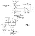
- Fig. 4 illustrates a variation of the circuitry shown in Fig. 2 in which the noise floor of the output signal is reduced to approximately 1 dB above the shot-noise level.
- the beam sampler 116 shown in Fig. 1 is selected to provide four times as much power in the sample beam 126 as is provided in the signal beam 128'.
- the proportion of the beam 111 that is reflected by the sampler 116 depends on the losses in the signal beam for the chosen application.
- a sample photocurrent is produced which has a signal to shot-noise ratio that is 6 dB greater than the signal to shot-noise ratio of the sample photocurrent produced by the embodiments shown in Figs. 2 and 3.
- a resistor network including resistors 410 and 412 is inserted between the collector electrode of the transistor Q2 and the summing junction 220 and a voltage source 414 has been inserted between the base electrode of transistor Q1 and ground.
- the resistors 410 and 412 shunt three-fourths of the sample photocurrent to ground so that only one-fourth of the detected sample photocurrent is passed to the summing junction 220.
- the effect of the voltage source 214 is to bias the transistor Q1 so that a current I C2 , which is substantially four times the signal photocurrent, can be passed by the transistor Q2.
- the voltage source 214 may be a variable voltage source which may be adjusted to produce a zero DC level in the output signal LO', or may be replaced by the feedback system of Fig. 3, including the servo amplifier.
- the signal to shot-noise ratio of the subdivided sample photocurrent that is applied to the summing junction 220 in this embodiment of the invention is 6 dB greater than the signal to shot-noise ratio of the sample photocurrents applied to the junction 220 in the previous embodiments.
- the resistor network does not degrade the signal to shot-noise ratio of the subdivided sample current. Consequently, the sum of the uncorrelated shot noise components of the signal and sample photocurrents at the summing junction 220 is only about 1 dB greater than the shot-noise component of the signal photocurrent alone.
- the circuit shown in Fig. 2 is modified by coupling an equal quantity of one or more diodes (not shown) in a forward-biased configuration, between the respective emitter electrodes of the transistors Q1 and Q2 and the junction 222. These diodes provide voltage feedback to correlate the currents I C1 and I C2 to achieve substantially the same shot noise reduction advantage as is achieved by the circuitry shown in Fig. 4.
- the system shown in Fig. 4 assumes that the loss in the optical system is large so that the splitting off #of the sample beam from the signal beam does not weaken the signal beam appreciably. Alternatively, the system assumes that excess laser power is available so that the sample beam may be made significantly more powerful than the signal beam without reducing the effectiveness of the signal beam.
- the optimal ratio between the sample and signal beams For weaker lasers and more efficient optical systems, it is useful to know the optimal ratio between the sample and signal beams.
- the method of selecting the optimum ratio assumes that the resistive divider formed by the transistors 410 and 412 is noiseless, that the current wasted through Q1 is negligible and that the noise to signal ratio in the output signal LO is the RMS sum of the noise to signal ratios of the sample and signal photocurrents.
- the optimal power reflectance, ⁇ opt of the beam sampler 116, for a given power efficiency, pe, of the optical system through which the signal beam provided by the beam sampler is to pass is given by equation (3).
- NF 20 log10(1 + ⁇ pe ⁇ ) (4)
- the sample beam should be limited to have a magnitude that is, for example, between 10% and 100% greater than is needed to cancel the signal photocurrent.
- the current division circuitry was configured to operate on the sample photocurrent. It is contemplated however that a differential pair of transistors (not shown) of opposite polarity to the transistors Q1 and Q2 may be used to subdivide the signal photocurrent in the same way that the transistors Q1 and Q2 subdivide the sample photocurrent. It is further contemplated two current dividers may be used in a feedback configuration such as that shown in Fig. 3 where output signals of one polarity are applied to the current divider coupled to receive the signal photocurrent while output signals of the other polarity are applied to the current divider coupled to receive the sample photocurrent. This configuration may be desirable when it is difficult to determine the maximum signal beam intensity at the detector.
- noise suppression systems described above are electronic devices, their primary application is in optical systems. Most laser-based optical systems are subject to excess laser noise and drift. Heroic measures are often taken to reduce the effects of these aberrations.
- noise suppression system examples include: infra-red absorption spectroscopy, using a lead salt diode laser; detection of phase features in photoresist and of particles having dimensions less than 0.1 micron through scanning optical microscopy; homodyne detection of submicron aerosol particles by light scattering or extinction; detection of residual stress in thin films by detecting stress-induced birefringence; and thermoreflectance thermometry.
- a noise suppression system according to this invention may also be beneficial in coherent detection LIDAR (optical radar), laser scanning microscopy of biological specimens and various forms of interferometry, especially those that involve fringe tracking.
- Some diode lasers exhibit position dependent noise due to the relatively low finesse of their resonators. Consequently, these lasers have relatively poor rejection of higher order Gaussian modes compared to most gas lasers. With lasers that exhibit a variation in noise level across the beam, it is important to ensure that both the signal and sample detectors see all of the beam cross section. With lasers that exhibit different levels of noise in different polarization states, it may be desirable to add a polarizer at the laser output to ensure that the sample and signal beams arise from the same polarization component of the beam produced by the laser.
Landscapes
- Physics & Mathematics (AREA)
- Engineering & Computer Science (AREA)
- Electromagnetism (AREA)
- General Physics & Mathematics (AREA)
- Radar, Positioning & Navigation (AREA)
- Remote Sensing (AREA)
- Computer Networks & Wireless Communication (AREA)
- Plasma & Fusion (AREA)
- Optics & Photonics (AREA)
- Spectroscopy & Molecular Physics (AREA)
- Investigating Or Analysing Materials By Optical Means (AREA)
- Lasers (AREA)
- Optical Radar Systems And Details Thereof (AREA)
- Photometry And Measurement Of Optical Pulse Characteristics (AREA)
Applications Claiming Priority (2)
| Application Number | Priority Date | Filing Date | Title |
|---|---|---|---|
| US07/594,178 US5134276A (en) | 1990-10-09 | 1990-10-09 | Noise cancelling circuitry for optical systems with signal dividing and combining means |
| US594178 | 1990-10-09 |
Publications (2)
| Publication Number | Publication Date |
|---|---|
| EP0480182A2 true EP0480182A2 (fr) | 1992-04-15 |
| EP0480182A3 EP0480182A3 (en) | 1992-05-20 |
Family
ID=24377849
Family Applications (1)
| Application Number | Title | Priority Date | Filing Date |
|---|---|---|---|
| EP19910115233 Withdrawn EP0480182A3 (en) | 1990-10-09 | 1991-09-10 | Noise cancelling circuitry for optical systems |
Country Status (3)
| Country | Link |
|---|---|
| US (1) | US5134276A (fr) |
| EP (1) | EP0480182A3 (fr) |
| JP (1) | JP2662113B2 (fr) |
Cited By (4)
| Publication number | Priority date | Publication date | Assignee | Title |
|---|---|---|---|---|
| CN105699955A (zh) * | 2014-12-09 | 2016-06-22 | 英特希尔美国公司 | 用于光学式邻近侦测器的精确度估计 |
| EP3255790A1 (fr) * | 2016-04-04 | 2017-12-13 | Biosense Webster (Israel), Ltd. | Amplificateur d'isolement linéaire avec annulation de la tension de sortie cc |
| US20200163562A1 (en) * | 2017-09-08 | 2020-05-28 | Intel Corporation | Low noise front-end for a heart rate monitor using photo-plethysmography |
| CN115684129A (zh) * | 2022-10-28 | 2023-02-03 | 嘉庚创新实验室 | 一种拉曼光谱信号降噪处理方法、装置及拉曼光谱仪 |
Families Citing this family (31)
| Publication number | Priority date | Publication date | Assignee | Title |
|---|---|---|---|---|
| US5540825A (en) * | 1993-08-02 | 1996-07-30 | Iowa State University Research Foundation, Inc. | Noise suppressing capillary separation system |
| DE69712053T2 (de) * | 1996-05-14 | 2002-11-14 | Honeywell International Inc., Morristown | Gegen umwelteinflüsse unempfindlicher optischer sensor mit verbesserter störsignalunterdrückung |
| US5793230A (en) * | 1997-02-26 | 1998-08-11 | Sandia Corporation | Sensor readout detector circuit |
| US6091504A (en) * | 1998-05-21 | 2000-07-18 | Square One Technology, Inc. | Method and apparatus for measuring gas concentration using a semiconductor laser |
| US6141136A (en) * | 1999-08-27 | 2000-10-31 | Kalibjian; Ralph | Active phase-shift control in optical-hybrid etalons |
| AU1751701A (en) | 1999-11-04 | 2001-05-14 | L'air Liquide, Societe Anonyme A Directoire Et Conseil De Surveillance Pour L'etude Et L'exploitation Des Procedes Georges Claude | Method for continuously monitoring chemical species and temperature in hot process gases |
| US7005645B2 (en) | 2001-11-30 | 2006-02-28 | Air Liquide America L.P. | Apparatus and methods for launching and receiving a broad wavelength range source |
| US6741348B2 (en) | 2002-04-29 | 2004-05-25 | The Curators Of The University Of Missouri | Ultrasensitive spectrophotometer |
| US20040120549A1 (en) * | 2002-12-24 | 2004-06-24 | Chung-Shan Institute Of Science And Technology | Half-plane predictive cancellation method for laser radar distance image noise |
| US7409117B2 (en) | 2004-02-11 | 2008-08-05 | American Air Liquide, Inc. | Dynamic laser power control for gas species monitoring |
| US7268881B2 (en) * | 2004-02-17 | 2007-09-11 | The Curators Of The University Of Missouri | Light scattering detector |
| US7903252B2 (en) * | 2005-01-13 | 2011-03-08 | The Curators Of The University Of Missouri | Noise cancellation in fourier transform spectrophotometry |
| US7262844B2 (en) * | 2005-01-13 | 2007-08-28 | The Curators Of The University Of Missouri | Ultrasensitive spectrophotometer |
| US7616316B1 (en) | 2006-02-27 | 2009-11-10 | Southwest Sciences Incorporated | Gas measurement over extreme dynamic range of concentrations |
| CN101755204A (zh) | 2006-03-09 | 2010-06-23 | 全技术联合公司 | 蒸发光散射检测器 |
| GB0624361D0 (en) * | 2006-12-06 | 2007-01-17 | Michelson Diagnostics Ltd | Multiple beam source for a multi-beam interferometer and multi-beam interferometer |
| US7710568B1 (en) | 2007-09-28 | 2010-05-04 | Southwest Sciences Incorporated | Portable natural gas leak detector |
| WO2009152321A1 (fr) * | 2008-06-11 | 2009-12-17 | The Curators Of The University Of Missouri | Détecteur de chromatographie en phase liquide et régulateur de débit pour ledit détecteur |
| US7920265B1 (en) | 2008-07-29 | 2011-04-05 | Kla-Tencor Corporation | Apparatus and method for noise reduction in modulated optical reflectance metrology system |
| US7943915B2 (en) * | 2008-10-10 | 2011-05-17 | Ge Infrastructure Sensing, Inc. | Method of calibrating a wavelength-modulation spectroscopy apparatus |
| US7957001B2 (en) * | 2008-10-10 | 2011-06-07 | Ge Infrastructure Sensing, Inc. | Wavelength-modulation spectroscopy method and apparatus |
| US8488973B2 (en) * | 2010-02-11 | 2013-07-16 | Silicon Audio, Inc. | Signal processing within an optical microphone |
| JP5666617B2 (ja) * | 2010-03-17 | 2015-02-12 | ライトラボ・イメージング・インコーポレーテッド | 干渉センシングおよび画像取得システムのための強度雑音を低減する方法および装置 |
| WO2012168239A1 (fr) | 2011-06-06 | 2012-12-13 | Carl Zeiss Meditec Ag | Systèmes et procédés pour la détection compensée améliorée en imagerie tomographique par cohérence optique |
| GB201114330D0 (en) * | 2011-08-19 | 2011-10-05 | Michelson Diagnostics Ltd | Detector circuits for interferometers |
| WO2015030202A1 (fr) * | 2013-08-30 | 2015-03-05 | 国立大学法人電気通信大学 | Dispositif de mesure optique, procédé de mesure optique, et système d'imagerie microscopique |
| US9494462B2 (en) | 2015-02-13 | 2016-11-15 | Northrop Grumman Systems Corporation | Balanced intensity differential photo detector |
| US10809128B2 (en) | 2017-03-31 | 2020-10-20 | The Regents Of The University Of California | General noise suppression scheme with reference detection in optical heterodyne spectroscopy |
| US10310085B2 (en) | 2017-07-07 | 2019-06-04 | Mezmeriz Inc. | Photonic integrated distance measuring pixel and method of distance measurement |
| JP7567112B2 (ja) * | 2020-05-18 | 2024-10-16 | 株式会社エーティーエー | 差分検出共役補償cars計測装置 |
| AT528255A1 (de) | 2024-04-30 | 2025-11-15 | Mio Hannes | Strukturanalysevorrichtung |
Family Cites Families (16)
| Publication number | Priority date | Publication date | Assignee | Title |
|---|---|---|---|---|
| US3446972A (en) * | 1966-07-18 | 1969-05-27 | Kollmorgen Corp | Automatic gain control for photomultiplier tubes employing a monitoring photocell |
| US3626092A (en) * | 1969-07-15 | 1971-12-07 | Ibm | Video amplifier for optical scanners |
| US4032801A (en) * | 1975-10-10 | 1977-06-28 | Honeywell Inc. | Electromagnetic radiation intensity comparator apparatus |
| JPS5379586A (en) * | 1976-12-23 | 1978-07-14 | Fujitsu Ltd | Photo detector bias circuit |
| DE2705308C2 (de) * | 1977-02-09 | 1979-04-19 | Bodenseewerk Perkin-Elmer & Co Gmbh, 7770 Ueberlingen | Vorrichtung zum Aufheizen eines Graphitrohres in einer Graphitrohrküvette eines Atomabsorptionsspektrometers |
| US4150402A (en) * | 1977-04-07 | 1979-04-17 | Xerox Corporation | Method and apparatus for reducing the effect of laser noise in a scanning laser read system |
| US4185278A (en) * | 1977-09-22 | 1980-01-22 | HF Systems, Incorporated | Obscuration type smoke detector |
| US4190747A (en) * | 1978-04-05 | 1980-02-26 | Bell Telephone Laboratories, Incorporated | Signal corrected optocoupled device |
| US4491730A (en) * | 1980-08-14 | 1985-01-01 | Panametrics, Inc. | Method and apparatus for feedback stabilized photometric detection in fluids |
| US4467203A (en) * | 1981-10-19 | 1984-08-21 | Panametrics, Inc. | Low noise amplifier and method for energy biased radiation sensitive receiver |
| US4485301A (en) * | 1982-02-01 | 1984-11-27 | Sprague Electric Company | Linear two-terminal integrated circuit photo sensor |
| JPS6129223A (ja) * | 1984-07-19 | 1986-02-10 | Matsushita Electric Ind Co Ltd | 光−電気変換回路 |
| GB2172164B (en) * | 1985-03-07 | 1989-02-22 | Stc Plc | Balanced coherent receiver |
| JPS63238452A (ja) * | 1987-03-26 | 1988-10-04 | Nec Corp | 光学式液質測定装置 |
| JPS6467073A (en) * | 1987-09-07 | 1989-03-13 | Fuji Photo Film Co Ltd | Picture signal correcting method |
| JP2641923B2 (ja) * | 1988-10-31 | 1997-08-20 | 日本電気株式会社 | 光受信器初段回路 |
-
1990
- 1990-10-09 US US07/594,178 patent/US5134276A/en not_active Expired - Lifetime
-
1991
- 1991-07-11 JP JP3196065A patent/JP2662113B2/ja not_active Expired - Fee Related
- 1991-09-10 EP EP19910115233 patent/EP0480182A3/en not_active Withdrawn
Cited By (4)
| Publication number | Priority date | Publication date | Assignee | Title |
|---|---|---|---|---|
| CN105699955A (zh) * | 2014-12-09 | 2016-06-22 | 英特希尔美国公司 | 用于光学式邻近侦测器的精确度估计 |
| EP3255790A1 (fr) * | 2016-04-04 | 2017-12-13 | Biosense Webster (Israel), Ltd. | Amplificateur d'isolement linéaire avec annulation de la tension de sortie cc |
| US20200163562A1 (en) * | 2017-09-08 | 2020-05-28 | Intel Corporation | Low noise front-end for a heart rate monitor using photo-plethysmography |
| CN115684129A (zh) * | 2022-10-28 | 2023-02-03 | 嘉庚创新实验室 | 一种拉曼光谱信号降噪处理方法、装置及拉曼光谱仪 |
Also Published As
| Publication number | Publication date |
|---|---|
| US5134276A (en) | 1992-07-28 |
| JP2662113B2 (ja) | 1997-10-08 |
| EP0480182A3 (en) | 1992-05-20 |
| JPH06341897A (ja) | 1994-12-13 |
Similar Documents
| Publication | Publication Date | Title |
|---|---|---|
| US5134276A (en) | Noise cancelling circuitry for optical systems with signal dividing and combining means | |
| Hobbs | Ultrasensitive laser measurements without tears | |
| US5123024A (en) | Apparatus and method for controlling the light intensity of a laser diode | |
| US4659930A (en) | Radiation hard visible light readout circuit | |
| US4263555A (en) | Signal detection system | |
| US7920265B1 (en) | Apparatus and method for noise reduction in modulated optical reflectance metrology system | |
| EP0452557B1 (fr) | Circuit de mesure du niveau d'un signal comprenant des moyens de correction de décalage | |
| US8867929B2 (en) | Optical receiver using single ended voltage offset measurement | |
| US9494462B2 (en) | Balanced intensity differential photo detector | |
| Fonck et al. | Low‐noise photodiode detector for optical fluctuation diagnostics | |
| US20240168140A1 (en) | Device for converting a photonic signal, associated lidar and method | |
| US4889985A (en) | Combined optical power meter and receiver | |
| US7939790B1 (en) | Method and apparatus for controlling the gain of an avalanche photodiode with fluctuations in temperature | |
| JP2001013005A (ja) | 光電変換率調節可能な光量検出回路 | |
| US20170048001A1 (en) | Apparatus and Method for Isolating an Optical Signal by Subtracting the Atmospheric Background in Real Time | |
| JPH0722209B2 (ja) | 光増幅器の絶対雑光指数決定装置および決定方法 | |
| US20200233065A1 (en) | Optical detector with dc compensation | |
| JP2001503145A (ja) | 装置のノイズ測定システム | |
| US5535044A (en) | Optical frequency mixing apparatus | |
| EP0460273A1 (fr) | Amplificateur à gain stabilisé | |
| US20070069822A1 (en) | Device for measuring very short current pulses | |
| Puryga et al. | Broadband Signal Amplification Paths for Semiconductor Radiation and Particle Detectors | |
| Cox et al. | Some limits on the performance of an analog optical link | |
| Seto et al. | Algorithm of auto-balancing noise-canceling based on noise correlation for high-speed balancing, high-dynamic range, and robustness against DC-offset drift | |
| Altmann et al. | Fast current amplifier for background-limited operation of photovoltaic InSb detectors |
Legal Events
| Date | Code | Title | Description |
|---|---|---|---|
| PUAI | Public reference made under article 153(3) epc to a published international application that has entered the european phase |
Free format text: ORIGINAL CODE: 0009012 |
|
| PUAL | Search report despatched |
Free format text: ORIGINAL CODE: 0009013 |
|
| AK | Designated contracting states |
Kind code of ref document: A2 Designated state(s): DE FR GB |
|
| AK | Designated contracting states |
Kind code of ref document: A3 Designated state(s): DE FR GB |
|
| STAA | Information on the status of an ep patent application or granted ep patent |
Free format text: STATUS: THE APPLICATION IS DEEMED TO BE WITHDRAWN |
|
| 18D | Application deemed to be withdrawn |
Effective date: 19921121 |