EP0480231B1 - Module optique émetteur-récepteur - Google Patents
Module optique émetteur-récepteur Download PDFInfo
- Publication number
- EP0480231B1 EP0480231B1 EP91116202A EP91116202A EP0480231B1 EP 0480231 B1 EP0480231 B1 EP 0480231B1 EP 91116202 A EP91116202 A EP 91116202A EP 91116202 A EP91116202 A EP 91116202A EP 0480231 B1 EP0480231 B1 EP 0480231B1
- Authority
- EP
- European Patent Office
- Prior art keywords
- optical
- resonator
- modulation
- transceiver module
- optical transceiver
- Prior art date
- Legal status (The legal status is an assumption and is not a legal conclusion. Google has not performed a legal analysis and makes no representation as to the accuracy of the status listed.)
- Expired - Lifetime
Links
- 230000003287 optical effect Effects 0.000 title claims description 66
- 230000005540 biological transmission Effects 0.000 claims description 23
- 238000000034 method Methods 0.000 claims description 3
- 230000010355 oscillation Effects 0.000 claims description 3
- 230000008878 coupling Effects 0.000 description 6
- 238000010168 coupling process Methods 0.000 description 6
- 238000005859 coupling reaction Methods 0.000 description 6
- 238000005452 bending Methods 0.000 description 3
- 239000003365 glass fiber Substances 0.000 description 3
- 238000005253 cladding Methods 0.000 description 1
- 238000004891 communication Methods 0.000 description 1
- 239000000835 fiber Substances 0.000 description 1
- 238000003384 imaging method Methods 0.000 description 1
- 230000000737 periodic effect Effects 0.000 description 1
- 239000010453 quartz Substances 0.000 description 1
- VYPSYNLAJGMNEJ-UHFFFAOYSA-N silicon dioxide Inorganic materials O=[Si]=O VYPSYNLAJGMNEJ-UHFFFAOYSA-N 0.000 description 1
Images

Classifications
-
- G—PHYSICS
- G02—OPTICS
- G02F—OPTICAL DEVICES OR ARRANGEMENTS FOR THE CONTROL OF LIGHT BY MODIFICATION OF THE OPTICAL PROPERTIES OF THE MEDIA OF THE ELEMENTS INVOLVED THEREIN; NON-LINEAR OPTICS; FREQUENCY-CHANGING OF LIGHT; OPTICAL LOGIC ELEMENTS; OPTICAL ANALOGUE/DIGITAL CONVERTERS
- G02F1/00—Devices or arrangements for the control of the intensity, colour, phase, polarisation or direction of light arriving from an independent light source, e.g. switching, gating or modulating; Non-linear optics
- G02F1/01—Devices or arrangements for the control of the intensity, colour, phase, polarisation or direction of light arriving from an independent light source, e.g. switching, gating or modulating; Non-linear optics for the control of the intensity, phase, polarisation or colour
- G02F1/21—Devices or arrangements for the control of the intensity, colour, phase, polarisation or direction of light arriving from an independent light source, e.g. switching, gating or modulating; Non-linear optics for the control of the intensity, phase, polarisation or colour by interference
-
- H—ELECTRICITY
- H01—ELECTRIC ELEMENTS
- H01S—DEVICES USING THE PROCESS OF LIGHT AMPLIFICATION BY STIMULATED EMISSION OF RADIATION [LASER] TO AMPLIFY OR GENERATE LIGHT; DEVICES USING STIMULATED EMISSION OF ELECTROMAGNETIC RADIATION IN WAVE RANGES OTHER THAN OPTICAL
- H01S3/00—Lasers, i.e. devices using stimulated emission of electromagnetic radiation in the infrared, visible or ultraviolet wave range
- H01S3/10—Controlling the intensity, frequency, phase, polarisation or direction of the emitted radiation, e.g. switching, gating, modulating or demodulating
- H01S3/105—Controlling the intensity, frequency, phase, polarisation or direction of the emitted radiation, e.g. switching, gating, modulating or demodulating by controlling the mutual position or the reflecting properties of the reflectors of the cavity, e.g. by controlling the cavity length
-
- H—ELECTRICITY
- H04—ELECTRIC COMMUNICATION TECHNIQUE
- H04B—TRANSMISSION
- H04B10/00—Transmission systems employing electromagnetic waves other than radio-waves, e.g. infrared, visible or ultraviolet light, or employing corpuscular radiation, e.g. quantum communication
- H04B10/25—Arrangements specific to fibre transmission
- H04B10/2589—Bidirectional transmission
- H04B10/25891—Transmission components
-
- G—PHYSICS
- G02—OPTICS
- G02F—OPTICAL DEVICES OR ARRANGEMENTS FOR THE CONTROL OF LIGHT BY MODIFICATION OF THE OPTICAL PROPERTIES OF THE MEDIA OF THE ELEMENTS INVOLVED THEREIN; NON-LINEAR OPTICS; FREQUENCY-CHANGING OF LIGHT; OPTICAL LOGIC ELEMENTS; OPTICAL ANALOGUE/DIGITAL CONVERTERS
- G02F1/00—Devices or arrangements for the control of the intensity, colour, phase, polarisation or direction of light arriving from an independent light source, e.g. switching, gating or modulating; Non-linear optics
- G02F1/01—Devices or arrangements for the control of the intensity, colour, phase, polarisation or direction of light arriving from an independent light source, e.g. switching, gating or modulating; Non-linear optics for the control of the intensity, phase, polarisation or colour
- G02F1/21—Devices or arrangements for the control of the intensity, colour, phase, polarisation or direction of light arriving from an independent light source, e.g. switching, gating or modulating; Non-linear optics for the control of the intensity, phase, polarisation or colour by interference
- G02F1/213—Fabry-Perot type
-
- G—PHYSICS
- G02—OPTICS
- G02F—OPTICAL DEVICES OR ARRANGEMENTS FOR THE CONTROL OF LIGHT BY MODIFICATION OF THE OPTICAL PROPERTIES OF THE MEDIA OF THE ELEMENTS INVOLVED THEREIN; NON-LINEAR OPTICS; FREQUENCY-CHANGING OF LIGHT; OPTICAL LOGIC ELEMENTS; OPTICAL ANALOGUE/DIGITAL CONVERTERS
- G02F2203/00—Function characteristic
- G02F2203/02—Function characteristic reflective
Definitions
- the invention relates to an optical transmission and reception module, a method for modulating the module and an optical transmission system with such modules.
- Such modulators are used in optical communication systems in which a line terminal device, without containing a light source, generates the signal to be transmitted.
- the optical carrier for such a transmission signal is generated in a center and fed to the line end device via an optical waveguide, modulated there, and the resulting transmission signal is preferably transmitted via the same optical waveguide.
- the described reflection modulator consists of an electro-optically active waveguide coupler which can be operated as a switch and is contained in an integrated optical circuit.
- the optical waveguide for message transmission is on a first one Connection of the first branch and the mirror surface arranged on a first connection of the second branch.
- light entering the modulator from the optical waveguide can be reflected back into the optical waveguide via the mirror surface. If one considers the light entering the modulator as an optical carrier and the switching as modulation, it can be said that an optical transmission signal is generated by modulating the carrier.
- the disadvantage of the known optical reflection modulator is that the adjustment between the optical waveguide and the integrated optical circuit in which the reflection modulator is located must be very precise and is technologically correspondingly complex.
- the invention has for its object to provide an optical reflection waveguide in which this disadvantage is eliminated.
- a particular advantage of the invention lies in the use of the reflection modulator in a transmission and reception module. It is advantageous that no coupler for dividing the carrier power is partly necessary for the photodiode and partly for the mirror surface, and that in the transmitting and receiving module, in the mode of operation as a transmitting module, no disturbing reflections from the surface of the photodiode are added to the transmitted signal become.
- Another advantage of the invention is that the required components are available on the market as series products.
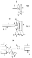
- the basic principle of the optical reflection modulator is shown in FIG. In the following, the optical reflection modulator is simply called the modulator for the sake of simplicity.
- the modulator 1 has the following parts: an end face of a optical waveguide 2 through which light emerges. This end surface is called second mirror surface 4 below.
- a first mirror surface 3 is arranged opposite it.
- the mirror surfaces 3 and 4 lie parallel to one another and thus form a Fabry-Perot resonator 5 with a resonator length x between the two mirror surfaces 3 and 4.
- the resonator length x is an optical length, ie the refractive index of a medium contained in the Fabry-Perot resonator 5 is taken into account.
- the variation of the resonator length x only represents a special type of detuning of the Fabry-Perot resonator 5.
- the resonator 5 can also be tilted out by one of the two Mirror surfaces 3, 4 out of their plane, or by deforming one of the two mirror surfaces 3, 4, or in another way or in combination of the above-mentioned possibilities.
- the implementation of a modulator using some of the aforementioned detuning options is shown below in the exemplary embodiments.
- the resonator 5 can contain imaging optics in the beam path between the two mirror surfaces 3 and 4.
- a glass fiber optical waveguide is advantageously used as the optical waveguide 2.
- the second mirror surface 4 is an end surface of the glass fiber optical waveguide, which is preferably at right angles to the glass fiber cladding.
- the quality of the resonator 5 can be adjusted by changing the reflectance of the mirror surfaces 3, 4 in a known manner, for example by applying selected layers.
- the modulator 20 has a thickness oscillator 8 in the form of a piezoelectric transducer with electrical connections 7, to which a modulation voltage U m , ie the modulation signal, can be applied.
- the first mirror surface 3 is connected to the piezoelectric transducer 8 in such a way that the resonator length x changes when the modulation voltage U m is applied .
- FIG. 4 shows the second exemplary embodiment of a modular gate 30, in which the detuning is likewise carried out by varying the resonator length x.
- a birefringent medium 9 is arranged between two electrodes E, to which the modulation voltage U m is applied, the refractive index n of which can be changed by applying the modulation voltage U m .
- the resonator length x changes due to the change in the refractive index of the medium 9.
- the first mirror surface 3 lies on a surface of the medium 9 which is at right angles to the surfaces on which the electrodes E bear.
- the second mirror surface 4 is located on the side of the medium 9 that lies opposite the first mirror surface 3.
- the third exemplary embodiment of a modular gate 10 is shown in FIG. 5.
- this modulator 10 only the thickness transducer 8 is replaced by a flexural transducer 6, preferably a quartz oscillator, compared to the modulator 20 from FIG. 3.
- the Fabry-Perot resonator 5 is detuned by a combination of the variation in the resonator length x and the tilting of the first mirror surface 3 out of its rest plane.
- FIG. 6 shows a transmission and reception module 40, which is provided with a modulator according to the invention, here the modulator 20 of the second exemplary embodiment.
- a modulator according to the invention, here the modulator 20 of the second exemplary embodiment.
- a signal diode for example a PIN photodiode, is arranged on the thickness transducer 8 for message signals.
- the first mirror surface 3 forms the entry surface of the light into the photodiode 11.
- the generated photocurrent I P flows through the connections 12.
- the photodiode 11 detects the incident light with the power P T minus the reflected portion. Since the generated photocurrent I P depends only slightly on the resonator length x, there is no disturbing modulation of the photocurrent I P by varying the resonator length x. A typical value of the disturbance is less than 1 dB.
- a particular advantage of the modulator 10, 20, 30 over the known modulator lies in the uncomplicated coupling between the optical waveguide 2 and the Fabry-Perot resonator 5.
- the modulators 10, 20, 30 only require coupling with the quality of an average waveguide -Photodiode coupling, whereas for the known modulator, due to its "integrated optical waveguide", a coupling with the higher quality of a waveguide-laser coupling is necessary.
- the arrangement of a bending oscillator 6 in a transmitting and receiving module 40 reduces the coupling problem compared to the known transmitting and receiving module at least in the direction of adjustment, which lies in the direction of movement of the bending oscillator 6.
- the complete mode of operation of the transmitting and receiving module is explained using an exemplary embodiment of an optical message transmission system ON.
- the reflected and modulated with the frequency f 1 signal is now transmitted via the same optical waveguide AL and the star distributor S to the central station Z and is fed there via an 3dB power coupler K to an optical receiver module E. This is followed by an electrical receiver that filters and demodulates the desired band, for example with the modulation frequency f 1.
- the operating point is preferably from one of the antinodes of the standing wave by the distance ⁇ 0 / 8.
- NRZ Network Return to Zero
- These signals can be amplitude, phase or frequency modulated.
- the optical message transmission system ON enables a single laser module L located in the center Z to supply a plurality of subscribers T i via the star distributor S, which in turn can transmit signals directed to the center Z by modulating the received carrier.
- the identification of the individual subscriber signals in the central Z is carried out by using different frequencies f 1 of the subcarrier.
- the transmission in the downward direction is broadband in the exemplary embodiment, e.g. for cable television and telephony; the transmission in the upward direction is narrowband, e.g. for telephony only.
- symmetrical broadband transmission is also possible, in particular when using the modulator 30 of the second exemplary embodiment.
Landscapes
- Physics & Mathematics (AREA)
- Electromagnetism (AREA)
- Optics & Photonics (AREA)
- Engineering & Computer Science (AREA)
- Nonlinear Science (AREA)
- Computer Networks & Wireless Communication (AREA)
- Plasma & Fusion (AREA)
- Signal Processing (AREA)
- General Physics & Mathematics (AREA)
- Mechanical Light Control Or Optical Switches (AREA)
- Optical Communication System (AREA)
- Semiconductor Lasers (AREA)
- Optical Modulation, Optical Deflection, Nonlinear Optics, Optical Demodulation, Optical Logic Elements (AREA)
Claims (11)
- Module optique émetteur-récepteur, comprenant un guide d'ondes (2) optique, un équipement de modulation et une photodiode (11),- où l'équipement de modulation contient un résonateur (5) optique dont l'accord peut être modifié, comprenant une première et une deuxième surface de miroir (3, 4), qui sont disposées l'une en face de l'autre, et où la deuxième surface de miroir (4) représente la surface extrême du guide d'ondes (2) optique,- où la lumière quittant la surface extrême du guide d'ondes (2) optique, après avoir parcouru le résonateur (5), peut être mise en évidence dans une photodiode (11) disposée derrière la première surface de miroir (3), et- où la lumière présente dans le résonateur (5) est couplée en réaction, par le biais de la deuxième surface miroir (4), dans le guide d'ondes (2) optique et, à titre de porteuse, peut être modulée avec un signal de modulation par une modification de l'accord du résonateur (5).
- Module optique émetteur-récepteur selon la revendication 1, caractérisé en ce que les normales de surface de la première et de la deuxième surface de miroir (3, 4) sont parallèles à l'état de repos, ce qui signifie que le résonateur (5) est un résonateur Fabry-Perot.
- Module optique émetteur-récepteur selon la revendication 1, caractérisé en ce que les normales de surface de la première et de la deuxième surface de miroir (3, 4) ne sont pas parallèles à l'état de repos.
- Module optique émetteur-récepteur selon l'une des revendications 1 à 3, caractérisé en ce que la longueur optique du résonateur peut être modifiée sous la commande du signal de modulation.
- Module optique émetteur-récepteur selon la revendication 4, caractérisé en ce que, entre les miroirs (3, 4), est disposé un milieu biréfringent (9) avec indice de réfraction variable, pour faire varier la longueur optique.
- Module optique émetteur-récepteur selon l'une des revendications 1 à 5, caractérisé en ce qu'au moins l'une des deux surfaces de miroir (3, 4) est disposée de façon à pouvoir opérer un déplacement angulaire sous la commande du signal de modulation.
- Module optique émetteur-récepteur selon l'une des revendications 1 à 6, caractérisé en ce que la première surface de miroir (3), pour faire varier l'accord du résonateur, est disposée sur un équipement oscillant (6, 8) mécanique pouvant être commandé par le signal de modulation.
- Module optique émetteur-récepteur selon la revendication 1, caractérisé en ce que la première surface de miroir (3) est la surface d'entrée de la lumière dans la photodiode (11).
- Procédé de modulation d'un module optique émetteur-récepteur selon l'une des revendications 1 à 8, caractérisé en ce que la modulation de la porteuse s'effectue avec une excursion de modulation de la longueur de résonateur (x) qui est supérieure à la demi-longueur d'onde (λ₀) de la porteuse.
- Procédé de modulation de la lumière au moyen d'un module optique émetteur-récepteur selon l'une des revendications 1 à 7, caractérisé en ce que la modulation s'effectue par variation de la longueur de résonateur (X) avec une excursion de modulation inférieure à un quart de la longueur d'onde λ₀ de la lumière et en ce que le point de travail est éloigné d'une distance λ₀/8 d'un des ventres d'oscillation de l'onde stationnaire.
- Système de transmission optique comprenant un central et plusieurs abonnés, dans lequel les abonnés sont équipés de modules optiques émetteur-récepteur selon l'une des revendications 1 à 8 pour la production d'un signal d'émission, dans lequel la porteuse du signal d'émission optique de plusieurs abonnés peut être produite dans un module laser du central et dans lequel cette porteuse peut être modulée chez les différents abonnés, la porteuse chez les différents abonnés (Ti, i = 1, 2, ... N) pouvant être munie d'une sous-porteuse et la fréquence des sous-porteuses des différents abonnés (Ti, i = 1, 2, ... N) étant différente.
Applications Claiming Priority (2)
| Application Number | Priority Date | Filing Date | Title |
|---|---|---|---|
| DE4031970A DE4031970A1 (de) | 1990-10-09 | 1990-10-09 | Optischer reflexionsmodulator |
| DE4031970 | 1990-10-09 |
Publications (3)
| Publication Number | Publication Date |
|---|---|
| EP0480231A2 EP0480231A2 (fr) | 1992-04-15 |
| EP0480231A3 EP0480231A3 (en) | 1992-06-10 |
| EP0480231B1 true EP0480231B1 (fr) | 1995-12-27 |
Family
ID=6415910
Family Applications (1)
| Application Number | Title | Priority Date | Filing Date |
|---|---|---|---|
| EP91116202A Expired - Lifetime EP0480231B1 (fr) | 1990-10-09 | 1991-09-24 | Module optique émetteur-récepteur |
Country Status (6)
| Country | Link |
|---|---|
| US (1) | US5253099A (fr) |
| EP (1) | EP0480231B1 (fr) |
| JP (1) | JPH04263212A (fr) |
| CA (1) | CA2053022C (fr) |
| DE (2) | DE4031970A1 (fr) |
| ES (1) | ES2084077T3 (fr) |
Families Citing this family (18)
| Publication number | Priority date | Publication date | Assignee | Title |
|---|---|---|---|---|
| WO1994006052A1 (fr) | 1992-09-10 | 1994-03-17 | Fujitsu Limited | Systeme de circuit optique et ses constituants |
| US6693736B1 (en) | 1992-09-10 | 2004-02-17 | Fujitsu Limited | Optical circuit system and components of same |
| EP0599375B1 (fr) * | 1992-11-20 | 1999-03-03 | Ascom Tech Ag | Modulateur de lumière |
| EP0599154A1 (fr) * | 1992-11-20 | 1994-06-01 | Ascom Tech Ag | Modulateur pour un faisceau de lumière |
| EP0729051A3 (fr) * | 1995-02-21 | 1998-06-17 | Ascom Tech Ag | Modulateur optique à réflection |
| US5796880A (en) * | 1996-11-18 | 1998-08-18 | Lucent Technologies Inc. | Technique for modulating optical signals in optical communications |
| US20060176916A1 (en) * | 2003-01-23 | 2006-08-10 | Eckhard Zanger | Laser resonator and frequency-converted laser |
| GB2399921B (en) * | 2003-03-26 | 2005-12-28 | Schlumberger Holdings | Borehole telemetry system |
| GB2418028B (en) * | 2003-05-07 | 2007-08-01 | Qinetiq Ltd | Dynamic optical reflector and interrogation system |
| US7606537B2 (en) * | 2004-02-10 | 2009-10-20 | Colin Dugald Brodhead | System and method for transmitting data via wave reflection |
| JP5017765B2 (ja) * | 2004-03-30 | 2012-09-05 | 日本電気株式会社 | 光変調器とその製造方法並びに変調光学系とこれを用いた光インターコネクト装置並びに光通信装置 |
| US7348893B2 (en) * | 2004-12-22 | 2008-03-25 | Schlumberger Technology Corporation | Borehole communication and measurement system |
| GB0515523D0 (en) * | 2005-07-28 | 2005-12-07 | Bae Systems Plc | Transponder |
| GB0521253D0 (en) * | 2005-10-19 | 2005-11-30 | Qinetiq Ltd | Optical angle detection |
| US8224189B1 (en) | 2007-02-02 | 2012-07-17 | Sunlight Photonics Inc. | Retro-directive target for free-space optical communication and method of producing the same |
| US8204384B2 (en) * | 2008-11-21 | 2012-06-19 | Cubic Corporation | Phase-modulating communication device |
| US8498502B2 (en) | 2010-12-17 | 2013-07-30 | Fujitsu Limited | Device for phase modulation |
| US11018778B1 (en) | 2020-05-20 | 2021-05-25 | Verizon Patent And Licensing Inc. | System and method to prevent unauthorized voice detection via fiber links |
Family Cites Families (11)
| Publication number | Priority date | Publication date | Assignee | Title |
|---|---|---|---|---|
| US4209689A (en) * | 1969-06-04 | 1980-06-24 | Hughes Aircraft Company | Laser secure communications system |
| US3863064A (en) * | 1972-01-03 | 1975-01-28 | Philco Ford Corp | Differential retrocommunicator |
| US4446543A (en) * | 1979-07-02 | 1984-05-01 | The United States Of America As Represented By The Secretary Of The Navy | Optical resonator single-mode fiber hydrophone |
| US4268116A (en) * | 1979-10-26 | 1981-05-19 | Optelecom Incorporated | Method and apparatus for radiant energy modulation in optical fibers |
| US4358851A (en) * | 1980-02-28 | 1982-11-09 | Xerox Corporation | Fiber optic laser device and light emitter utilizing the device |
| US4577924A (en) * | 1982-06-03 | 1986-03-25 | General Dynamics Electronics Division | Optical recursive filter |
| US4744625A (en) * | 1982-09-30 | 1988-05-17 | Gte Laboratories Incorporated | Methods of and apparatus for providing frequency modulated light |
| US4533829A (en) * | 1983-07-07 | 1985-08-06 | The United States Of America As Represented By The Secretary Of The Air Force | Optical electromagnetic radiation detector |
| US4937833A (en) * | 1985-03-25 | 1990-06-26 | The United States Of America As Represented By The Secretary Of The Navy | Analog frequency modulated laser using magnetostriction |
| FR2585849B1 (fr) * | 1985-07-30 | 1988-12-30 | Suisse Electro Microtech Centr | Systeme de detection a fibre optique incorporant un capteur a modulation d'intensite |
| GB2190789B (en) * | 1986-04-17 | 1990-05-09 | Plessey Co Plc | System for optically coupling components of integrated circuits |
-
1990
- 1990-10-09 DE DE4031970A patent/DE4031970A1/de not_active Withdrawn
-
1991
- 1991-09-16 US US07/760,469 patent/US5253099A/en not_active Expired - Fee Related
- 1991-09-24 DE DE59107145T patent/DE59107145D1/de not_active Expired - Fee Related
- 1991-09-24 ES ES91116202T patent/ES2084077T3/es not_active Expired - Lifetime
- 1991-09-24 EP EP91116202A patent/EP0480231B1/fr not_active Expired - Lifetime
- 1991-09-30 JP JP3278668A patent/JPH04263212A/ja active Pending
- 1991-10-08 CA CA002053022A patent/CA2053022C/fr not_active Expired - Fee Related
Also Published As
| Publication number | Publication date |
|---|---|
| ES2084077T3 (es) | 1996-05-01 |
| CA2053022A1 (fr) | 1992-04-10 |
| US5253099A (en) | 1993-10-12 |
| EP0480231A3 (en) | 1992-06-10 |
| EP0480231A2 (fr) | 1992-04-15 |
| DE59107145D1 (de) | 1996-02-08 |
| JPH04263212A (ja) | 1992-09-18 |
| CA2053022C (fr) | 1998-11-24 |
| DE4031970A1 (de) | 1992-04-16 |
Similar Documents
| Publication | Publication Date | Title |
|---|---|---|
| EP0480231B1 (fr) | Module optique émetteur-récepteur | |
| DE3232430C2 (de) | Optisches Nachrichtenübertragungssystem | |
| DE69320101T2 (de) | Unterdrücken von Rauschen und Verzerrungen in einem Lichtwellenleitersystem | |
| DE3787902T2 (de) | Optischer Sender mit einem optischen Frequenzdiskriminator. | |
| DE60222889T2 (de) | Wellenlängensteuerung mit dither-modulation und rückkopplung | |
| DE69032875T2 (de) | Optische Verteilung von analogen und digitalen Signalen mittels optischen Modulatoren mit komplementären Ausgängen | |
| DE69007812T2 (de) | Laser mit verteilter Rückkoppelung für frequenzmodulierte Kommunikationssysteme. | |
| DE3501967C2 (de) | Optische Datenverbindung | |
| EP0383138A2 (fr) | Dispositif pour la réception optique directe d'une pluralité de longueurs d'ondes | |
| DE69611995T2 (de) | Verfahren und vorrichtung zur übertragung von signalen in optischen fasern | |
| DE4415176A1 (de) | Vorrichtung und Verfahren zur Dispersionskompensation in einem faseroptischen Übertragungssystem | |
| EP0096327A1 (fr) | Réseau de distribution | |
| EP0354567A2 (fr) | Ensemble émission-réception pour un système de communication bidirectionnel cohérent et optique | |
| DE19722370A1 (de) | Empfänger für ein optisches Nachrichtenübertragungssystem und Verfahren zu dessen Betrieb | |
| DE69221457T2 (de) | Einrichtung, in der Frequenzerhöhung von elektromagnetischer Strahlung auftritt, und eine solche Einrichtung enthaltendes Gerät zum optischen Abtasten einer Informationsebene | |
| DE3637809A1 (de) | Sender fuer kohaerente lichtwellen | |
| DE60308244T2 (de) | Verfahren und Vorrichtung zur Erzeugung eines optischen Pulszugs mit unterdrücktem Träger und Gitter-Vorrichtung | |
| EP0644668B1 (fr) | Module d'émmission-réception pour transmission bidirectionnelle optique à plusieurs canaux | |
| DE69114282T2 (de) | Optischer signalregenerator und optisches übertragungssystem, das diesen benutzt. | |
| EP0349766A2 (fr) | Système de transmission d'informations optique, concernant en particulier le raccordement d'abonnés | |
| EP0320688B1 (fr) | Dispositif émetteur-récepteur à rétroréflexion pour système de communication bidirectionnel à fibre optique | |
| EP1378074B1 (fr) | Dispositif et systeme de transmission optique de donnees entre des satellites | |
| US5526159A (en) | Method and circuit arrangement for electric compensation of signal distortion caused by laser chirp and fiber dispersion | |
| DE60107088T2 (de) | Ein CS-RZ optischer Taktgenerator und ein resynchronisierter optischer Multiplexer, der solch einen Generator enthält | |
| DE60200221T2 (de) | Optischer Sender, System und Verfahren zur Übertragung von Signalen mit hohen Datenraten |
Legal Events
| Date | Code | Title | Description |
|---|---|---|---|
| PUAI | Public reference made under article 153(3) epc to a published international application that has entered the european phase |
Free format text: ORIGINAL CODE: 0009012 |
|
| AK | Designated contracting states |
Kind code of ref document: A2 Designated state(s): BE CH DE ES FR GB IT LI NL |
|
| PUAL | Search report despatched |
Free format text: ORIGINAL CODE: 0009013 |
|
| AK | Designated contracting states |
Kind code of ref document: A3 Designated state(s): BE CH DE ES FR GB IT LI NL |
|
| 17P | Request for examination filed |
Effective date: 19920520 |
|
| RAP3 | Party data changed (applicant data changed or rights of an application transferred) |
Owner name: ALCATEL N.V. Owner name: ALCATEL SEL AKTIENGESELLSCHAFT |
|
| 17Q | First examination report despatched |
Effective date: 19931130 |
|
| GRAA | (expected) grant |
Free format text: ORIGINAL CODE: 0009210 |
|
| AK | Designated contracting states |
Kind code of ref document: B1 Designated state(s): BE CH DE ES FR GB IT LI NL |
|
| REF | Corresponds to: |
Ref document number: 59107145 Country of ref document: DE Date of ref document: 19960208 |
|
| REG | Reference to a national code |
Ref country code: CH Ref legal event code: NV Representative=s name: JUERG ULRICH C/O ALCATEL STR AG |
|
| ITF | It: translation for a ep patent filed | ||
| GBT | Gb: translation of ep patent filed (gb section 77(6)(a)/1977) |
Effective date: 19960222 |
|
| ET | Fr: translation filed | ||
| REG | Reference to a national code |
Ref country code: ES Ref legal event code: FG2A Ref document number: 2084077 Country of ref document: ES Kind code of ref document: T3 |
|
| PLBE | No opposition filed within time limit |
Free format text: ORIGINAL CODE: 0009261 |
|
| STAA | Information on the status of an ep patent application or granted ep patent |
Free format text: STATUS: NO OPPOSITION FILED WITHIN TIME LIMIT |
|
| 26N | No opposition filed | ||
| PGFP | Annual fee paid to national office [announced via postgrant information from national office to epo] |
Ref country code: GB Payment date: 20000814 Year of fee payment: 10 |
|
| PGFP | Annual fee paid to national office [announced via postgrant information from national office to epo] |
Ref country code: CH Payment date: 20000816 Year of fee payment: 10 |
|
| PGFP | Annual fee paid to national office [announced via postgrant information from national office to epo] |
Ref country code: NL Payment date: 20000824 Year of fee payment: 10 |
|
| PGFP | Annual fee paid to national office [announced via postgrant information from national office to epo] |
Ref country code: DE Payment date: 20000830 Year of fee payment: 10 |
|
| PGFP | Annual fee paid to national office [announced via postgrant information from national office to epo] |
Ref country code: FR Payment date: 20000831 Year of fee payment: 10 |
|
| PGFP | Annual fee paid to national office [announced via postgrant information from national office to epo] |
Ref country code: BE Payment date: 20000911 Year of fee payment: 10 |
|
| PGFP | Annual fee paid to national office [announced via postgrant information from national office to epo] |
Ref country code: ES Payment date: 20000922 Year of fee payment: 10 |
|
| PG25 | Lapsed in a contracting state [announced via postgrant information from national office to epo] |
Ref country code: GB Free format text: LAPSE BECAUSE OF NON-PAYMENT OF DUE FEES Effective date: 20010924 |
|
| PG25 | Lapsed in a contracting state [announced via postgrant information from national office to epo] |
Ref country code: ES Free format text: LAPSE BECAUSE OF NON-PAYMENT OF DUE FEES Effective date: 20010925 |
|
| PG25 | Lapsed in a contracting state [announced via postgrant information from national office to epo] |
Ref country code: LI Free format text: LAPSE BECAUSE OF NON-PAYMENT OF DUE FEES Effective date: 20010930 Ref country code: CH Free format text: LAPSE BECAUSE OF NON-PAYMENT OF DUE FEES Effective date: 20010930 Ref country code: BE Free format text: LAPSE BECAUSE OF NON-PAYMENT OF DUE FEES Effective date: 20010930 |
|
| REG | Reference to a national code |
Ref country code: GB Ref legal event code: IF02 |
|
| BERE | Be: lapsed |
Owner name: ALCATEL N.V. Effective date: 20010930 |
|
| PG25 | Lapsed in a contracting state [announced via postgrant information from national office to epo] |
Ref country code: NL Free format text: LAPSE BECAUSE OF NON-PAYMENT OF DUE FEES Effective date: 20020401 |
|
| PG25 | Lapsed in a contracting state [announced via postgrant information from national office to epo] |
Ref country code: DE Free format text: LAPSE BECAUSE OF NON-PAYMENT OF DUE FEES Effective date: 20020501 |
|
| GBPC | Gb: european patent ceased through non-payment of renewal fee |
Effective date: 20010924 |
|
| REG | Reference to a national code |
Ref country code: CH Ref legal event code: PL |
|
| PG25 | Lapsed in a contracting state [announced via postgrant information from national office to epo] |
Ref country code: FR Free format text: LAPSE BECAUSE OF NON-PAYMENT OF DUE FEES Effective date: 20020531 |
|
| NLV4 | Nl: lapsed or anulled due to non-payment of the annual fee |
Effective date: 20020401 |
|
| REG | Reference to a national code |
Ref country code: FR Ref legal event code: ST |
|
| NLV4 | Nl: lapsed or anulled due to non-payment of the annual fee |
Effective date: 20020401 |
|
| REG | Reference to a national code |
Ref country code: ES Ref legal event code: FD2A Effective date: 20021011 |
|
| PG25 | Lapsed in a contracting state [announced via postgrant information from national office to epo] |
Ref country code: IT Free format text: LAPSE BECAUSE OF NON-PAYMENT OF DUE FEES;WARNING: LAPSES OF ITALIAN PATENTS WITH EFFECTIVE DATE BEFORE 2007 MAY HAVE OCCURRED AT ANY TIME BEFORE 2007. THE CORRECT EFFECTIVE DATE MAY BE DIFFERENT FROM THE ONE RECORDED. Effective date: 20050924 |