EP0480274B1 - Wahrnehmung und Messung von Beschleunigung - Google Patents
Wahrnehmung und Messung von Beschleunigung Download PDFInfo
- Publication number
- EP0480274B1 EP0480274B1 EP91116641A EP91116641A EP0480274B1 EP 0480274 B1 EP0480274 B1 EP 0480274B1 EP 91116641 A EP91116641 A EP 91116641A EP 91116641 A EP91116641 A EP 91116641A EP 0480274 B1 EP0480274 B1 EP 0480274B1
- Authority
- EP
- European Patent Office
- Prior art keywords
- layer
- thin metal
- signal
- metal layer
- spacer
- Prior art date
- Legal status (The legal status is an assumption and is not a legal conclusion. Google has not performed a legal analysis and makes no representation as to the accuracy of the status listed.)
- Expired - Lifetime
Links
- 230000001133 acceleration Effects 0.000 title description 11
- 238000005259 measurement Methods 0.000 title description 2
- 238000000034 method Methods 0.000 claims description 18
- 229910052751 metal Inorganic materials 0.000 claims description 14
- 239000002184 metal Substances 0.000 claims description 14
- 230000008569 process Effects 0.000 claims description 11
- 125000006850 spacer group Chemical group 0.000 claims description 10
- 239000000758 substrate Substances 0.000 claims description 8
- 238000004519 manufacturing process Methods 0.000 claims description 6
- WFKWXMTUELFFGS-UHFFFAOYSA-N tungsten Chemical compound [W] WFKWXMTUELFFGS-UHFFFAOYSA-N 0.000 claims description 6
- 229910052721 tungsten Inorganic materials 0.000 claims description 6
- 239000010937 tungsten Substances 0.000 claims description 6
- 229910000838 Al alloy Inorganic materials 0.000 claims description 3
- XAGFODPZIPBFFR-UHFFFAOYSA-N aluminium Chemical compound [Al] XAGFODPZIPBFFR-UHFFFAOYSA-N 0.000 claims description 3
- 229920000642 polymer Polymers 0.000 claims description 3
- 229910052710 silicon Inorganic materials 0.000 claims description 3
- 239000010703 silicon Substances 0.000 claims description 3
- 229910052782 aluminium Inorganic materials 0.000 claims description 2
- 229910001385 heavy metal Inorganic materials 0.000 claims 6
- 238000000059 patterning Methods 0.000 claims 3
- 238000000151 deposition Methods 0.000 claims 2
- 238000001020 plasma etching Methods 0.000 claims 1
- 238000009987 spinning Methods 0.000 claims 1
- 230000007704 transition Effects 0.000 description 6
- 230000001419 dependent effect Effects 0.000 description 3
- 238000012545 processing Methods 0.000 description 3
- 239000004065 semiconductor Substances 0.000 description 3
- KRHYYFGTRYWZRS-UHFFFAOYSA-N Fluorane Chemical compound F KRHYYFGTRYWZRS-UHFFFAOYSA-N 0.000 description 2
- VYPSYNLAJGMNEJ-UHFFFAOYSA-N Silicium dioxide Chemical compound O=[Si]=O VYPSYNLAJGMNEJ-UHFFFAOYSA-N 0.000 description 2
- 238000010586 diagram Methods 0.000 description 2
- 238000010237 hybrid technique Methods 0.000 description 2
- 239000000463 material Substances 0.000 description 2
- 229910044991 metal oxide Inorganic materials 0.000 description 2
- 150000004706 metal oxides Chemical class 0.000 description 2
- XUIMIQQOPSSXEZ-UHFFFAOYSA-N Silicon Chemical compound [Si] XUIMIQQOPSSXEZ-UHFFFAOYSA-N 0.000 description 1
- 239000004411 aluminium Substances 0.000 description 1
- 230000000295 complement effect Effects 0.000 description 1
- 230000002950 deficient Effects 0.000 description 1
- 238000001514 detection method Methods 0.000 description 1
- 238000006073 displacement reaction Methods 0.000 description 1
- 230000000694 effects Effects 0.000 description 1
- 238000011156 evaluation Methods 0.000 description 1
- 230000006872 improvement Effects 0.000 description 1
- 239000012528 membrane Substances 0.000 description 1
- 229910021421 monocrystalline silicon Inorganic materials 0.000 description 1
- 229910021420 polycrystalline silicon Inorganic materials 0.000 description 1
- 238000011002 quantification Methods 0.000 description 1
- 230000004044 response Effects 0.000 description 1
- 230000035945 sensitivity Effects 0.000 description 1
- 235000012239 silicon dioxide Nutrition 0.000 description 1
- 239000000377 silicon dioxide Substances 0.000 description 1
- 230000026683 transduction Effects 0.000 description 1
- 238000010361 transduction Methods 0.000 description 1
- 238000001039 wet etching Methods 0.000 description 1
Images


Classifications
-
- G—PHYSICS
- G01—MEASURING; TESTING
- G01P—MEASURING LINEAR OR ANGULAR SPEED, ACCELERATION, DECELERATION, OR SHOCK; INDICATING PRESENCE, ABSENCE, OR DIRECTION, OF MOVEMENT
- G01P3/00—Measuring linear or angular speed; Measuring differences of linear or angular speeds
- G01P3/36—Devices characterised by the use of optical means, e.g. using infrared, visible, or ultraviolet light
-
- G—PHYSICS
- G01—MEASURING; TESTING
- G01P—MEASURING LINEAR OR ANGULAR SPEED, ACCELERATION, DECELERATION, OR SHOCK; INDICATING PRESENCE, ABSENCE, OR DIRECTION, OF MOVEMENT
- G01P15/00—Measuring acceleration; Measuring deceleration; Measuring shock, i.e. sudden change of acceleration
- G01P15/02—Measuring acceleration; Measuring deceleration; Measuring shock, i.e. sudden change of acceleration by making use of inertia forces using solid seismic masses
- G01P15/08—Measuring acceleration; Measuring deceleration; Measuring shock, i.e. sudden change of acceleration by making use of inertia forces using solid seismic masses with conversion into electric or magnetic values
- G01P15/135—Measuring acceleration; Measuring deceleration; Measuring shock, i.e. sudden change of acceleration by making use of inertia forces using solid seismic masses with conversion into electric or magnetic values by making use of contacts which are actuated by a movable inertial mass
-
- B—PERFORMING OPERATIONS; TRANSPORTING
- B81—MICROSTRUCTURAL TECHNOLOGY
- B81B—MICROSTRUCTURAL DEVICES OR SYSTEMS, e.g. MICROMECHANICAL DEVICES
- B81B3/00—Devices comprising flexible or deformable elements, e.g. comprising elastic tongues or membranes
- B81B3/0002—Arrangements for avoiding sticking of the flexible or moving parts
-
- B—PERFORMING OPERATIONS; TRANSPORTING
- B81—MICROSTRUCTURAL TECHNOLOGY
- B81C—PROCESSES OR APPARATUS SPECIALLY ADAPTED FOR THE MANUFACTURE OR TREATMENT OF MICROSTRUCTURAL DEVICES OR SYSTEMS
- B81C1/00—Manufacture or treatment of devices or systems in or on a substrate
- B81C1/00015—Manufacture or treatment of devices or systems in or on a substrate for manufacturing microsystems
- B81C1/00222—Integrating an electronic processing unit with a micromechanical structure
- B81C1/00246—Monolithic integration, i.e. micromechanical structure and electronic processing unit are integrated on the same substrate
-
- G—PHYSICS
- G01—MEASURING; TESTING
- G01P—MEASURING LINEAR OR ANGULAR SPEED, ACCELERATION, DECELERATION, OR SHOCK; INDICATING PRESENCE, ABSENCE, OR DIRECTION, OF MOVEMENT
- G01P15/00—Measuring acceleration; Measuring deceleration; Measuring shock, i.e. sudden change of acceleration
- G01P15/02—Measuring acceleration; Measuring deceleration; Measuring shock, i.e. sudden change of acceleration by making use of inertia forces using solid seismic masses
- G01P15/08—Measuring acceleration; Measuring deceleration; Measuring shock, i.e. sudden change of acceleration by making use of inertia forces using solid seismic masses with conversion into electric or magnetic values
- G01P15/0802—Details
-
- B—PERFORMING OPERATIONS; TRANSPORTING
- B81—MICROSTRUCTURAL TECHNOLOGY
- B81B—MICROSTRUCTURAL DEVICES OR SYSTEMS, e.g. MICROMECHANICAL DEVICES
- B81B2201/00—Specific applications of microelectromechanical systems
- B81B2201/02—Sensors
- B81B2201/0228—Inertial sensors
- B81B2201/0235—Accelerometers
Definitions
- This invention relates to a structure having the features of claim 1. This structure is suitable for being used as an accelerator sensor element. Further, the invention relates to a process for fabrication of such a sensor element.
- the accelerometers in use are typically of one of two types.
- the first type uses strain-sensing techniques. These have piezo-electric or piezo-resistive material that senses either the stress induced by the inertial mass, or the strain induced by the spring supporting the mass.
- the second type are position-sensing. These measure the displacement of an accelerated mass connected to a restoring spring.
- accelerometers typically have a sensor element with a mass on the order of a gram. Hybrid techniques are necessary to integrate the transducer with the readout circuitry. These two factors contribute to two problems with this type of accelerometers. They are large in size, by integrated circuit standards. Also, they require expensive tail-end processing, making them expensive by semiconductor industry standards.
- accelerometers typically have masses and springs fabricated from single crystal or polycrystalline silicon.
- the sensors are on a silicon dioxide membrane.
- the silicon substrate is etched away with an anisotropic or orientation-dependent etch.
- the supporting oxide is then freed by wet-etching with hydrofluoric acid.
- Document US-A-4,855,544 discloses a micro-mechanically produced accelerator consisting of a plurality of individual sensor cells responsive to different levels of acceleration. This structure containing the sensor cells is not provided with any additional circuitry for addressing the cells and for processing the signals generated by the cells.
- Document FR-A- 2 626 077 discloses a plurality of deflection elements which are connected to an evaluation circuit which is not described to be fabricated in the substrate on which the deflection elements are formed.
- FIGURE 1 shows the block diagram of the accelerometer chip.
- FIGURE 2 is a cross-sectional view of a single accelerometer element showing the circuit.
- FIGURE 3 shows a portion of the addressing and encoding circuitry.
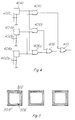
- FIGURE 4 shows the fault tolerant circuitry.
- FIGURE 5 shows the top view of a portion of the accelerometer element array.
- FIGURE 6 shows the processing levels in a cross-section of a single element.
- FIG. 1 is a block diagram of the accelerometer.
- the CMOS (Complementary Metal Oxide Semiconductor) shift register 102 pulses the array of deflection elements 104. If an element is deflected, it grounds the shift register pulse, causing a high signal to be passed to the comparator array 106. If an element is not deflected, the a low pulse is passed.
- the deflection elements are constructed such that they progress from a higher mass to a lower mass. This enables the elements in the array to be deflected by lower accelerations and the elements with a lower mass require higher accelerations. Each acceleration then has a set of masses it is capable of deflecting, and a set that it is not capable of deflecting.
- the comparator array 106 then compares the incoming signals for a difference between two, one low and one high. This is the transition point of the acceleration. The transition point is then passed on as a high signal to the decoder 108. The decoder then takes the high signal and generates a unique seven-bit word corresponding to the value of the acceleration.
- Figure 2 shows a cross-sectional view of one of the elements in the deflection array.
- Line 210 is pulsed high from the shift register. If mass 202 is sufficiently deflected on hinge 204, it touches contact 206. This then grounds the line 212, sending a low signal. This causes the transistor 214 to turn off and pass a high signal onto line 208.
- Line 208 connects to the comparator array circuitry, which includes latches to hold the deflection element output.
- CMOS N-channel Metal Oxide Semiconductor decoding and addressing circuitry
- the CMOS shift register 302 pulses high signals. If element 304B is deflected and touches grounded contact 306B, the high signal is grounded and a high signal is passed. Latch 308B is used to hold the signals for the comparator array.
- the signal is latched at 308B, it is passed into the exclusive OR gates (XOR) 310B and 310A. At the same time the signal from deflection element 304A is latched into 308A. The signal from 308A is then passed to the XOR gate 310A. If the signals from 308A and 308B ar both low, 310A will output a low signal. If 308B is low (deflected), and 308A is high (undeflected), and the fault checking shows this to be a true transition, the output will be a high signal. The high signal is then passed into the decoding circuitry. Through a series of transistors uniquely jumpered together as seen by 312, the single high signal is used to generate a unique digital word. This word is output through the wires 314.
- XOR exclusive OR gates
- Figure 4 shows an embodiment of fault tolerant circuitry using the redundant elements 402A, 402B and 462C.
- the monolithic manufacture of these elements reduces the possibility of defective elements and increases the chip yield. Yet it is still wise to incorporate some method for checking for stuck elements. The increased yield allows for redundant columns of elements to be produced.
- FIG. 5 A top view of a few of the deflection elements is shown in Figure 5.
- the mass 506, in this case tungsten is supported on hinges 502.
- the hinges are sitting on support metal 508.
- the support posts used in typical flexure beam deformable mirror devices (DMDs) can be used, but are not necessary. Since the only output of interest is the contact made at the underlying surface, the degree of deflection is not important, as long as contact is made.
- a side view of the sensor elements are shown in Figure 6.
- the fabrication process is very similar to that of DMDs.
- the address circuitry 612 is built upon the ground plane 610.
- the oxide contact 608 is then fabricated upon the address circuitry.
- a polymer spacer 604 is spun on the entire wafer.
- a thin layer of hinge aluminium 602 is deposited and the deflection element 614, including hinges and plate is photolithographically patterned and plasma etched.
- a thick layer of tungsten is deposited and formed differently for each element as the deflection mass 606.
- the deflection differences can be done in one of many ways.
- the tungsten can be patterned so a different mass is on each deflection element.
- different thickness of hinges can be used with the same masses on each. Either method will achieve the desired effect of a different deflection for each element, dependent on the acceleration.
- the element consists of a square of aluminum alloy approximately 50 »m on a side.
- the square is supported on four sides by narrow hinges. This causes the square to be limited to movement only up and down in a piston-like movement.
- Modelling of the architecture indicates that sensitivity to accelerations in the range 1 m/s2 to 100 m/s2 can be obtained with hinges approximately 50 »m long, 1 »m wide and 650 ⁇ thick.
- the mass of the element is determined by a photolithographically patterned tungsten mass 1-2 »m thick deposited on the aluminum element.
Landscapes
- Engineering & Computer Science (AREA)
- Physics & Mathematics (AREA)
- General Physics & Mathematics (AREA)
- Manufacturing & Machinery (AREA)
- Microelectronics & Electronic Packaging (AREA)
- Computer Hardware Design (AREA)
- Electromagnetism (AREA)
- Power Engineering (AREA)
- Pressure Sensors (AREA)
- Micromachines (AREA)
Claims (15)
- Struktur, enthaltend das folgende:a) ein Substrat;b) eine Adressierungsschaltung mit einem Schieberegister zur Erzeugung eines Signals, einen Transistor zum Empfangen dieses Signals, einen Zwischenspeicher zum Empfangen eines von dem Transistor erzeugten Signals;c) eine auf dem Substrat angebrachte Masseebene;d) eine Abstandsschicht, die über die Adressierungsschaltung eine Mulde bildet;e) eine von der Abstandsschicht getragene dünne Metallschicht, wobei die dünne Metallschicht Scharniere enthält, die einen mit ihnen verbunden Zentralbereich festlegen;f) einen elektrischen Kontakt, der auf der Adressierungsschaltung gebildet ist, so daß der Zentralbereich der dünnen Metallschicht dann, wenn er abgelenkt wird, eine elektrische Verbindung mit dem elektrischen Kontakt herstellt und ein Signal erzeugt, wobei die von der Abstandsschicht gebildete Mulde auch über dem elektrischen Kontakt liegt;g) eine Schicht aus schwerem Metall, die auf der dünnen Metallschicht gebildet ist, wobei die schwere Metallschicht so strukturiert ist, daß sie nur den Zentralbereich der dünnen Metallschicht bedeckt.
- Struktur nach Anspruch 1, bei welcher das Substrat aus Silizium besteht.
- Struktur nach Anspruch 1, bei welcher die Adressierungsschaltung eine CMOS-Schaltung ist.
- Struktur nach Anspruch 1, bei welcher der Kontaktpunkt eine Aluminiumlegierung ist.
- Struktur nach Anspruch 1, bei welcher die Abstandsschicht ein durch Plasmaätzen entfernbarer Polymer ist.
- Struktur nach Anspruch 1, bei welchem das dünne Metall eine Aluminiumlegierung ist.
- Struktur nach Anspruch 1, bei welcher das schwere Metall Wolfram ist.
- Verfahren zum Herstellen von Sensorelementen, die aus Strukturen gemäß einem der Ansprüche 1-7 bestehen, enthaltend das folgenende:a) Bilden einer Masse ebenen Schicht auf einem Scheibensubstrat;b) Herstellen einer Adressierungsschaltung und elektrischer Kontakte auf der Masseebene, wobei die Adressierungsschaltung einen Schieberegister zum Erzeugen eines Signals, einen Transistor zum Empfangen dieses Signals, einen Zwischenspeicher zum Empfangen eines von dem Transistor erzeugten Signals und ein Logikgatter zum Interpretieren des Transsistorsignals enthält;c) Aufschleudern einer Abstandsschicht auf die gesamte Scheibe;d) Ablagern einer Schicht aus einem dünnen Metall auf der Abstandsschicht ;e) Strukturieren der dünnen Metallschicht in der Weise, daß mehrere Zentralbereiche gebildet werden, die mit von der dünnen Metallschicht getragenen Scharnieren verbunden sind, die jeweils ein Ablenkelement repräsentieren;f) Ablagern einer Schicht aus einem schweren Metall auf der dünnen Metallschicht;g) Bilden mehrerer Chips auf der Scheibe;h) Strukturieren und Bilden der schweren Metallschicht, in der Weise, daß mehrere Ablenkelemente eines Chips eine unterschiedliche Masse haben;i) Unterteilen der Scheibe in einzelne Chips;j) Unterätzen der dünnen Metallschicht im Bereich jedes Ablenkelements, so daß die Abstandsschicht eine über der Adressierungsschaltung und dem jedem Ablenkelement zugeordneten elektrischen Kontakt angeordnete Mulde bildet.
- Verfahren nach Anspruch 8, bei welchem das Substrat aus Silizium besteht.
- Verfahren nach Anspruch 8, bei welchem die Adressierungsschaltung eine CMOS-Schaltung ist und die elektrischen Kontakte aus Oxid bestehen.
- Verfahren nach Anspruch 8, bei welchem die Abstandsschicht ein Polymer ist.
- Verfahren nach Anspruch 8, bei welchem das dünne Metall Aluminium ist.
- Verfahren nach Anspruch 8, bei welchem das Unterätzen ein Plasmaätzen ist.
- Verfahren nach Anspruch 8, bei welchem das schwere Metall Wolfram ist.
- Verfahren nach Anspruch 8, bei welchem das Strukturieren der dünnen Metallschicht photolithographisch erfolgt.
Priority Applications (1)
| Application Number | Priority Date | Filing Date | Title |
|---|---|---|---|
| EP94105604A EP0613009A3 (de) | 1990-10-12 | 1991-09-30 | System zur Feststellung und Messung von Beschleunigung. |
Applications Claiming Priority (2)
| Application Number | Priority Date | Filing Date | Title |
|---|---|---|---|
| US07/596,841 US5192395A (en) | 1990-10-12 | 1990-10-12 | Method of making a digital flexure beam accelerometer |
| US596841 | 1996-02-05 |
Related Child Applications (1)
| Application Number | Title | Priority Date | Filing Date |
|---|---|---|---|
| EP94105604.6 Division-Into | 1991-09-30 |
Publications (2)
| Publication Number | Publication Date |
|---|---|
| EP0480274A1 EP0480274A1 (de) | 1992-04-15 |
| EP0480274B1 true EP0480274B1 (de) | 1995-04-26 |
Family
ID=24388936
Family Applications (2)
| Application Number | Title | Priority Date | Filing Date |
|---|---|---|---|
| EP91116641A Expired - Lifetime EP0480274B1 (de) | 1990-10-12 | 1991-09-30 | Wahrnehmung und Messung von Beschleunigung |
| EP94105604A Withdrawn EP0613009A3 (de) | 1990-10-12 | 1991-09-30 | System zur Feststellung und Messung von Beschleunigung. |
Family Applications After (1)
| Application Number | Title | Priority Date | Filing Date |
|---|---|---|---|
| EP94105604A Withdrawn EP0613009A3 (de) | 1990-10-12 | 1991-09-30 | System zur Feststellung und Messung von Beschleunigung. |
Country Status (6)
| Country | Link |
|---|---|
| US (2) | US5192395A (de) |
| EP (2) | EP0480274B1 (de) |
| JP (1) | JPH0661509A (de) |
| KR (1) | KR100221296B1 (de) |
| DE (1) | DE69109225T2 (de) |
| TW (1) | TW275727B (de) |
Families Citing this family (192)
| Publication number | Priority date | Publication date | Assignee | Title |
|---|---|---|---|---|
| US5526688A (en) * | 1990-10-12 | 1996-06-18 | Texas Instruments Incorporated | Digital flexure beam accelerometer and method |
| DE69317462T2 (de) * | 1992-04-30 | 1998-08-27 | Texas Instruments Inc | Digitaler Beschleunigungsmesser |
| US6674562B1 (en) | 1994-05-05 | 2004-01-06 | Iridigm Display Corporation | Interferometric modulation of radiation |
| US5445412A (en) * | 1994-03-07 | 1995-08-29 | Automotive Systems Laboratory, Inc. | Vehicle impact detection system |
| DE4411130A1 (de) * | 1994-03-30 | 1995-10-05 | Siemens Ag | Sensoreinheit mit mindestens einem Beschleunigungssensor, z. B. zur Kfz-Airbagauslösung, und Verfahren zu seiner Herstellung |
| US6680792B2 (en) * | 1994-05-05 | 2004-01-20 | Iridigm Display Corporation | Interferometric modulation of radiation |
| US7460291B2 (en) | 1994-05-05 | 2008-12-02 | Idc, Llc | Separable modulator |
| US7297471B1 (en) | 2003-04-15 | 2007-11-20 | Idc, Llc | Method for manufacturing an array of interferometric modulators |
| US7138984B1 (en) | 2001-06-05 | 2006-11-21 | Idc, Llc | Directly laminated touch sensitive screen |
| US7550794B2 (en) * | 2002-09-20 | 2009-06-23 | Idc, Llc | Micromechanical systems device comprising a displaceable electrode and a charge-trapping layer |
| US8014059B2 (en) * | 1994-05-05 | 2011-09-06 | Qualcomm Mems Technologies, Inc. | System and method for charge control in a MEMS device |
| US7123216B1 (en) * | 1994-05-05 | 2006-10-17 | Idc, Llc | Photonic MEMS and structures |
| US5591910A (en) * | 1994-06-03 | 1997-01-07 | Texas Instruments Incorporated | Accelerometer |
| CA2149933A1 (en) | 1994-06-29 | 1995-12-30 | Robert M. Boysel | Micro-mechanical accelerometers with improved detection circuitry |
| US5658636A (en) * | 1995-01-27 | 1997-08-19 | Carnegie Mellon University | Method to prevent adhesion of micromechanical structures |
| US5659195A (en) * | 1995-06-08 | 1997-08-19 | The Regents Of The University Of California | CMOS integrated microsensor with a precision measurement circuit |
| US7471444B2 (en) * | 1996-12-19 | 2008-12-30 | Idc, Llc | Interferometric modulation of radiation |
| DE19842378C2 (de) * | 1997-09-20 | 2000-12-28 | Stoeger Automation Gmbh | Pneumatisches Handschraubgerät |
| US6058778A (en) * | 1997-10-24 | 2000-05-09 | Stmicroelectronics, Inc. | Integrated sensor having plurality of released beams for sensing acceleration |
| US8928967B2 (en) | 1998-04-08 | 2015-01-06 | Qualcomm Mems Technologies, Inc. | Method and device for modulating light |
| WO1999052006A2 (en) | 1998-04-08 | 1999-10-14 | Etalon, Inc. | Interferometric modulation of radiation |
| US7532377B2 (en) | 1998-04-08 | 2009-05-12 | Idc, Llc | Movable micro-electromechanical device |
| WO2003007049A1 (en) * | 1999-10-05 | 2003-01-23 | Iridigm Display Corporation | Photonic mems and structures |
| US6962771B1 (en) * | 2000-10-13 | 2005-11-08 | Taiwan Semiconductor Manufacturing Company, Ltd. | Dual damascene process |
| US6589625B1 (en) | 2001-08-01 | 2003-07-08 | Iridigm Display Corporation | Hermetic seal and method to create the same |
| US6794119B2 (en) * | 2002-02-12 | 2004-09-21 | Iridigm Display Corporation | Method for fabricating a structure for a microelectromechanical systems (MEMS) device |
| US6574033B1 (en) | 2002-02-27 | 2003-06-03 | Iridigm Display Corporation | Microelectromechanical systems device and method for fabricating same |
| US7781850B2 (en) * | 2002-09-20 | 2010-08-24 | Qualcomm Mems Technologies, Inc. | Controlling electromechanical behavior of structures within a microelectromechanical systems device |
| TW200413810A (en) | 2003-01-29 | 2004-08-01 | Prime View Int Co Ltd | Light interference display panel and its manufacturing method |
| TW594360B (en) * | 2003-04-21 | 2004-06-21 | Prime View Int Corp Ltd | A method for fabricating an interference display cell |
| TW570896B (en) | 2003-05-26 | 2004-01-11 | Prime View Int Co Ltd | A method for fabricating an interference display cell |
| US7221495B2 (en) * | 2003-06-24 | 2007-05-22 | Idc Llc | Thin film precursor stack for MEMS manufacturing |
| TW200506479A (en) * | 2003-08-15 | 2005-02-16 | Prime View Int Co Ltd | Color changeable pixel for an interference display |
| TWI231865B (en) * | 2003-08-26 | 2005-05-01 | Prime View Int Co Ltd | An interference display cell and fabrication method thereof |
| TWI232333B (en) * | 2003-09-03 | 2005-05-11 | Prime View Int Co Ltd | Display unit using interferometric modulation and manufacturing method thereof |
| TW593126B (en) | 2003-09-30 | 2004-06-21 | Prime View Int Co Ltd | A structure of a micro electro mechanical system and manufacturing the same |
| US7012726B1 (en) | 2003-11-03 | 2006-03-14 | Idc, Llc | MEMS devices with unreleased thin film components |
| US7142346B2 (en) | 2003-12-09 | 2006-11-28 | Idc, Llc | System and method for addressing a MEMS display |
| US7161728B2 (en) | 2003-12-09 | 2007-01-09 | Idc, Llc | Area array modulation and lead reduction in interferometric modulators |
| US7532194B2 (en) * | 2004-02-03 | 2009-05-12 | Idc, Llc | Driver voltage adjuster |
| US7119945B2 (en) | 2004-03-03 | 2006-10-10 | Idc, Llc | Altering temporal response of microelectromechanical elements |
| US7706050B2 (en) * | 2004-03-05 | 2010-04-27 | Qualcomm Mems Technologies, Inc. | Integrated modulator illumination |
| US7720148B2 (en) * | 2004-03-26 | 2010-05-18 | The Hong Kong University Of Science And Technology | Efficient multi-frame motion estimation for video compression |
| US7476327B2 (en) * | 2004-05-04 | 2009-01-13 | Idc, Llc | Method of manufacture for microelectromechanical devices |
| US7060895B2 (en) * | 2004-05-04 | 2006-06-13 | Idc, Llc | Modifying the electro-mechanical behavior of devices |
| US7164520B2 (en) * | 2004-05-12 | 2007-01-16 | Idc, Llc | Packaging for an interferometric modulator |
| US7256922B2 (en) * | 2004-07-02 | 2007-08-14 | Idc, Llc | Interferometric modulators with thin film transistors |
| TWI233916B (en) * | 2004-07-09 | 2005-06-11 | Prime View Int Co Ltd | A structure of a micro electro mechanical system |
| KR101313117B1 (ko) * | 2004-07-29 | 2013-09-30 | 퀄컴 엠이엠에스 테크놀로지스, 인크. | 간섭 변조기의 미소기전 동작을 위한 시스템 및 방법 |
| US7551159B2 (en) | 2004-08-27 | 2009-06-23 | Idc, Llc | System and method of sensing actuation and release voltages of an interferometric modulator |
| US7889163B2 (en) * | 2004-08-27 | 2011-02-15 | Qualcomm Mems Technologies, Inc. | Drive method for MEMS devices |
| US7560299B2 (en) * | 2004-08-27 | 2009-07-14 | Idc, Llc | Systems and methods of actuating MEMS display elements |
| US7515147B2 (en) * | 2004-08-27 | 2009-04-07 | Idc, Llc | Staggered column drive circuit systems and methods |
| US7499208B2 (en) | 2004-08-27 | 2009-03-03 | Udc, Llc | Current mode display driver circuit realization feature |
| US7602375B2 (en) * | 2004-09-27 | 2009-10-13 | Idc, Llc | Method and system for writing data to MEMS display elements |
| US7719500B2 (en) * | 2004-09-27 | 2010-05-18 | Qualcomm Mems Technologies, Inc. | Reflective display pixels arranged in non-rectangular arrays |
| US7327510B2 (en) | 2004-09-27 | 2008-02-05 | Idc, Llc | Process for modifying offset voltage characteristics of an interferometric modulator |
| US7304784B2 (en) * | 2004-09-27 | 2007-12-04 | Idc, Llc | Reflective display device having viewable display on both sides |
| US7813026B2 (en) * | 2004-09-27 | 2010-10-12 | Qualcomm Mems Technologies, Inc. | System and method of reducing color shift in a display |
| US7920135B2 (en) * | 2004-09-27 | 2011-04-05 | Qualcomm Mems Technologies, Inc. | Method and system for driving a bi-stable display |
| US20060065366A1 (en) * | 2004-09-27 | 2006-03-30 | Cummings William J | Portable etch chamber |
| WO2006037044A1 (en) * | 2004-09-27 | 2006-04-06 | Idc, Llc | Method and device for multistate interferometric light modulation |
| US7675669B2 (en) | 2004-09-27 | 2010-03-09 | Qualcomm Mems Technologies, Inc. | Method and system for driving interferometric modulators |
| US7369296B2 (en) * | 2004-09-27 | 2008-05-06 | Idc, Llc | Device and method for modifying actuation voltage thresholds of a deformable membrane in an interferometric modulator |
| US7349136B2 (en) * | 2004-09-27 | 2008-03-25 | Idc, Llc | Method and device for a display having transparent components integrated therein |
| US7460246B2 (en) * | 2004-09-27 | 2008-12-02 | Idc, Llc | Method and system for sensing light using interferometric elements |
| US7130104B2 (en) * | 2004-09-27 | 2006-10-31 | Idc, Llc | Methods and devices for inhibiting tilting of a mirror in an interferometric modulator |
| US7355780B2 (en) | 2004-09-27 | 2008-04-08 | Idc, Llc | System and method of illuminating interferometric modulators using backlighting |
| US7692839B2 (en) * | 2004-09-27 | 2010-04-06 | Qualcomm Mems Technologies, Inc. | System and method of providing MEMS device with anti-stiction coating |
| US20060076634A1 (en) | 2004-09-27 | 2006-04-13 | Lauren Palmateer | Method and system for packaging MEMS devices with incorporated getter |
| US7359066B2 (en) * | 2004-09-27 | 2008-04-15 | Idc, Llc | Electro-optical measurement of hysteresis in interferometric modulators |
| US7446927B2 (en) * | 2004-09-27 | 2008-11-04 | Idc, Llc | MEMS switch with set and latch electrodes |
| US7343080B2 (en) | 2004-09-27 | 2008-03-11 | Idc, Llc | System and method of testing humidity in a sealed MEMS device |
| US7583429B2 (en) | 2004-09-27 | 2009-09-01 | Idc, Llc | Ornamental display device |
| US7710629B2 (en) * | 2004-09-27 | 2010-05-04 | Qualcomm Mems Technologies, Inc. | System and method for display device with reinforcing substance |
| US7259449B2 (en) * | 2004-09-27 | 2007-08-21 | Idc, Llc | Method and system for sealing a substrate |
| US7936497B2 (en) * | 2004-09-27 | 2011-05-03 | Qualcomm Mems Technologies, Inc. | MEMS device having deformable membrane characterized by mechanical persistence |
| US8878825B2 (en) * | 2004-09-27 | 2014-11-04 | Qualcomm Mems Technologies, Inc. | System and method for providing a variable refresh rate of an interferometric modulator display |
| US7545550B2 (en) * | 2004-09-27 | 2009-06-09 | Idc, Llc | Systems and methods of actuating MEMS display elements |
| US7653371B2 (en) * | 2004-09-27 | 2010-01-26 | Qualcomm Mems Technologies, Inc. | Selectable capacitance circuit |
| US7417783B2 (en) * | 2004-09-27 | 2008-08-26 | Idc, Llc | Mirror and mirror layer for optical modulator and method |
| US7535466B2 (en) * | 2004-09-27 | 2009-05-19 | Idc, Llc | System with server based control of client device display features |
| US20060176487A1 (en) * | 2004-09-27 | 2006-08-10 | William Cummings | Process control monitors for interferometric modulators |
| US7289259B2 (en) * | 2004-09-27 | 2007-10-30 | Idc, Llc | Conductive bus structure for interferometric modulator array |
| US20060077126A1 (en) * | 2004-09-27 | 2006-04-13 | Manish Kothari | Apparatus and method for arranging devices into an interconnected array |
| US7345805B2 (en) * | 2004-09-27 | 2008-03-18 | Idc, Llc | Interferometric modulator array with integrated MEMS electrical switches |
| US8310441B2 (en) | 2004-09-27 | 2012-11-13 | Qualcomm Mems Technologies, Inc. | Method and system for writing data to MEMS display elements |
| US20060065622A1 (en) * | 2004-09-27 | 2006-03-30 | Floyd Philip D | Method and system for xenon fluoride etching with enhanced efficiency |
| US7299681B2 (en) * | 2004-09-27 | 2007-11-27 | Idc, Llc | Method and system for detecting leak in electronic devices |
| US7368803B2 (en) * | 2004-09-27 | 2008-05-06 | Idc, Llc | System and method for protecting microelectromechanical systems array using back-plate with non-flat portion |
| US20060067650A1 (en) * | 2004-09-27 | 2006-03-30 | Clarence Chui | Method of making a reflective display device using thin film transistor production techniques |
| US7916103B2 (en) | 2004-09-27 | 2011-03-29 | Qualcomm Mems Technologies, Inc. | System and method for display device with end-of-life phenomena |
| US20060066932A1 (en) * | 2004-09-27 | 2006-03-30 | Clarence Chui | Method of selective etching using etch stop layer |
| US7679627B2 (en) | 2004-09-27 | 2010-03-16 | Qualcomm Mems Technologies, Inc. | Controller and driver features for bi-stable display |
| US7302157B2 (en) * | 2004-09-27 | 2007-11-27 | Idc, Llc | System and method for multi-level brightness in interferometric modulation |
| US7136213B2 (en) * | 2004-09-27 | 2006-11-14 | Idc, Llc | Interferometric modulators having charge persistence |
| US7424198B2 (en) * | 2004-09-27 | 2008-09-09 | Idc, Llc | Method and device for packaging a substrate |
| US7369294B2 (en) * | 2004-09-27 | 2008-05-06 | Idc, Llc | Ornamental display device |
| US7564612B2 (en) * | 2004-09-27 | 2009-07-21 | Idc, Llc | Photonic MEMS and structures |
| US20060103643A1 (en) * | 2004-09-27 | 2006-05-18 | Mithran Mathew | Measuring and modeling power consumption in displays |
| US7586484B2 (en) * | 2004-09-27 | 2009-09-08 | Idc, Llc | Controller and driver features for bi-stable display |
| US7429334B2 (en) * | 2004-09-27 | 2008-09-30 | Idc, Llc | Methods of fabricating interferometric modulators by selectively removing a material |
| US7668415B2 (en) * | 2004-09-27 | 2010-02-23 | Qualcomm Mems Technologies, Inc. | Method and device for providing electronic circuitry on a backplate |
| US7893919B2 (en) | 2004-09-27 | 2011-02-22 | Qualcomm Mems Technologies, Inc. | Display region architectures |
| US7373026B2 (en) * | 2004-09-27 | 2008-05-13 | Idc, Llc | MEMS device fabricated on a pre-patterned substrate |
| US7554714B2 (en) * | 2004-09-27 | 2009-06-30 | Idc, Llc | Device and method for manipulation of thermal response in a modulator |
| US7724993B2 (en) * | 2004-09-27 | 2010-05-25 | Qualcomm Mems Technologies, Inc. | MEMS switches with deforming membranes |
| US7453579B2 (en) | 2004-09-27 | 2008-11-18 | Idc, Llc | Measurement of the dynamic characteristics of interferometric modulators |
| US7843410B2 (en) * | 2004-09-27 | 2010-11-30 | Qualcomm Mems Technologies, Inc. | Method and device for electrically programmable display |
| US7161730B2 (en) | 2004-09-27 | 2007-01-09 | Idc, Llc | System and method for providing thermal compensation for an interferometric modulator display |
| US7372613B2 (en) | 2004-09-27 | 2008-05-13 | Idc, Llc | Method and device for multistate interferometric light modulation |
| US7317568B2 (en) * | 2004-09-27 | 2008-01-08 | Idc, Llc | System and method of implementation of interferometric modulators for display mirrors |
| US7310179B2 (en) | 2004-09-27 | 2007-12-18 | Idc, Llc | Method and device for selective adjustment of hysteresis window |
| US8124434B2 (en) * | 2004-09-27 | 2012-02-28 | Qualcomm Mems Technologies, Inc. | Method and system for packaging a display |
| US7289256B2 (en) * | 2004-09-27 | 2007-10-30 | Idc, Llc | Electrical characterization of interferometric modulators |
| US7532195B2 (en) * | 2004-09-27 | 2009-05-12 | Idc, Llc | Method and system for reducing power consumption in a display |
| US7630119B2 (en) * | 2004-09-27 | 2009-12-08 | Qualcomm Mems Technologies, Inc. | Apparatus and method for reducing slippage between structures in an interferometric modulator |
| US7420725B2 (en) | 2004-09-27 | 2008-09-02 | Idc, Llc | Device having a conductive light absorbing mask and method for fabricating same |
| US20060066596A1 (en) * | 2004-09-27 | 2006-03-30 | Sampsell Jeffrey B | System and method of transmitting video data |
| US7321456B2 (en) * | 2004-09-27 | 2008-01-22 | Idc, Llc | Method and device for corner interferometric modulation |
| US7944599B2 (en) | 2004-09-27 | 2011-05-17 | Qualcomm Mems Technologies, Inc. | Electromechanical device with optical function separated from mechanical and electrical function |
| US7405924B2 (en) | 2004-09-27 | 2008-07-29 | Idc, Llc | System and method for protecting microelectromechanical systems array using structurally reinforced back-plate |
| US7808703B2 (en) * | 2004-09-27 | 2010-10-05 | Qualcomm Mems Technologies, Inc. | System and method for implementation of interferometric modulator displays |
| US7553684B2 (en) * | 2004-09-27 | 2009-06-30 | Idc, Llc | Method of fabricating interferometric devices using lift-off processing techniques |
| US7405861B2 (en) * | 2004-09-27 | 2008-07-29 | Idc, Llc | Method and device for protecting interferometric modulators from electrostatic discharge |
| US8008736B2 (en) * | 2004-09-27 | 2011-08-30 | Qualcomm Mems Technologies, Inc. | Analog interferometric modulator device |
| US7527995B2 (en) * | 2004-09-27 | 2009-05-05 | Qualcomm Mems Technologies, Inc. | Method of making prestructure for MEMS systems |
| US7417735B2 (en) * | 2004-09-27 | 2008-08-26 | Idc, Llc | Systems and methods for measuring color and contrast in specular reflective devices |
| US7415186B2 (en) * | 2004-09-27 | 2008-08-19 | Idc, Llc | Methods for visually inspecting interferometric modulators for defects |
| US7492502B2 (en) * | 2004-09-27 | 2009-02-17 | Idc, Llc | Method of fabricating a free-standing microstructure |
| US7626581B2 (en) * | 2004-09-27 | 2009-12-01 | Idc, Llc | Device and method for display memory using manipulation of mechanical response |
| US7684104B2 (en) * | 2004-09-27 | 2010-03-23 | Idc, Llc | MEMS using filler material and method |
| US7701631B2 (en) * | 2004-09-27 | 2010-04-20 | Qualcomm Mems Technologies, Inc. | Device having patterned spacers for backplates and method of making the same |
| US20060066594A1 (en) * | 2004-09-27 | 2006-03-30 | Karen Tyger | Systems and methods for driving a bi-stable display element |
| TW200628877A (en) * | 2005-02-04 | 2006-08-16 | Prime View Int Co Ltd | Method of manufacturing optical interference type color display |
| US7920136B2 (en) * | 2005-05-05 | 2011-04-05 | Qualcomm Mems Technologies, Inc. | System and method of driving a MEMS display device |
| KR20080027236A (ko) | 2005-05-05 | 2008-03-26 | 콸콤 인코포레이티드 | 다이나믹 드라이버 ic 및 디스플레이 패널 구성 |
| US7948457B2 (en) * | 2005-05-05 | 2011-05-24 | Qualcomm Mems Technologies, Inc. | Systems and methods of actuating MEMS display elements |
| US20060277486A1 (en) * | 2005-06-02 | 2006-12-07 | Skinner David N | File or user interface element marking system |
| CA2616268A1 (en) | 2005-07-22 | 2007-02-01 | Qualcomm Incorporated | Mems devices having support structures and methods of fabricating the same |
| WO2007013939A1 (en) * | 2005-07-22 | 2007-02-01 | Qualcomm Incorporated | Support structure for mems device and methods therefor |
| EP2495212A3 (de) | 2005-07-22 | 2012-10-31 | QUALCOMM MEMS Technologies, Inc. | MEMS-Vorrichtungen mit Stützstrukturen und Herstellungsverfahren dafür |
| US7355779B2 (en) * | 2005-09-02 | 2008-04-08 | Idc, Llc | Method and system for driving MEMS display elements |
| US7630114B2 (en) * | 2005-10-28 | 2009-12-08 | Idc, Llc | Diffusion barrier layer for MEMS devices |
| US8391630B2 (en) * | 2005-12-22 | 2013-03-05 | Qualcomm Mems Technologies, Inc. | System and method for power reduction when decompressing video streams for interferometric modulator displays |
| US7795061B2 (en) | 2005-12-29 | 2010-09-14 | Qualcomm Mems Technologies, Inc. | Method of creating MEMS device cavities by a non-etching process |
| US7636151B2 (en) * | 2006-01-06 | 2009-12-22 | Qualcomm Mems Technologies, Inc. | System and method for providing residual stress test structures |
| US7916980B2 (en) | 2006-01-13 | 2011-03-29 | Qualcomm Mems Technologies, Inc. | Interconnect structure for MEMS device |
| US7382515B2 (en) * | 2006-01-18 | 2008-06-03 | Qualcomm Mems Technologies, Inc. | Silicon-rich silicon nitrides as etch stops in MEMS manufacture |
| US8194056B2 (en) * | 2006-02-09 | 2012-06-05 | Qualcomm Mems Technologies Inc. | Method and system for writing data to MEMS display elements |
| US7582952B2 (en) * | 2006-02-21 | 2009-09-01 | Qualcomm Mems Technologies, Inc. | Method for providing and removing discharging interconnect for chip-on-glass output leads and structures thereof |
| US7547568B2 (en) * | 2006-02-22 | 2009-06-16 | Qualcomm Mems Technologies, Inc. | Electrical conditioning of MEMS device and insulating layer thereof |
| US7550810B2 (en) * | 2006-02-23 | 2009-06-23 | Qualcomm Mems Technologies, Inc. | MEMS device having a layer movable at asymmetric rates |
| US7450295B2 (en) * | 2006-03-02 | 2008-11-11 | Qualcomm Mems Technologies, Inc. | Methods for producing MEMS with protective coatings using multi-component sacrificial layers |
| US7643203B2 (en) | 2006-04-10 | 2010-01-05 | Qualcomm Mems Technologies, Inc. | Interferometric optical display system with broadband characteristics |
| US7903047B2 (en) * | 2006-04-17 | 2011-03-08 | Qualcomm Mems Technologies, Inc. | Mode indicator for interferometric modulator displays |
| US20070249078A1 (en) * | 2006-04-19 | 2007-10-25 | Ming-Hau Tung | Non-planar surface structures and process for microelectromechanical systems |
| US7417784B2 (en) * | 2006-04-19 | 2008-08-26 | Qualcomm Mems Technologies, Inc. | Microelectromechanical device and method utilizing a porous surface |
| US7527996B2 (en) * | 2006-04-19 | 2009-05-05 | Qualcomm Mems Technologies, Inc. | Non-planar surface structures and process for microelectromechanical systems |
| US7623287B2 (en) * | 2006-04-19 | 2009-11-24 | Qualcomm Mems Technologies, Inc. | Non-planar surface structures and process for microelectromechanical systems |
| US7711239B2 (en) | 2006-04-19 | 2010-05-04 | Qualcomm Mems Technologies, Inc. | Microelectromechanical device and method utilizing nanoparticles |
| US8049713B2 (en) * | 2006-04-24 | 2011-11-01 | Qualcomm Mems Technologies, Inc. | Power consumption optimized display update |
| US7369292B2 (en) * | 2006-05-03 | 2008-05-06 | Qualcomm Mems Technologies, Inc. | Electrode and interconnect materials for MEMS devices |
| US7649671B2 (en) * | 2006-06-01 | 2010-01-19 | Qualcomm Mems Technologies, Inc. | Analog interferometric modulator device with electrostatic actuation and release |
| US7405863B2 (en) * | 2006-06-01 | 2008-07-29 | Qualcomm Mems Technologies, Inc. | Patterning of mechanical layer in MEMS to reduce stresses at supports |
| US7321457B2 (en) | 2006-06-01 | 2008-01-22 | Qualcomm Incorporated | Process and structure for fabrication of MEMS device having isolated edge posts |
| US7471441B1 (en) | 2006-06-09 | 2008-12-30 | Hewlett-Packard Development Company, L.P. | Flexures |
| US7471442B2 (en) * | 2006-06-15 | 2008-12-30 | Qualcomm Mems Technologies, Inc. | Method and apparatus for low range bit depth enhancements for MEMS display architectures |
| US7702192B2 (en) | 2006-06-21 | 2010-04-20 | Qualcomm Mems Technologies, Inc. | Systems and methods for driving MEMS display |
| US7835061B2 (en) * | 2006-06-28 | 2010-11-16 | Qualcomm Mems Technologies, Inc. | Support structures for free-standing electromechanical devices |
| US7385744B2 (en) * | 2006-06-28 | 2008-06-10 | Qualcomm Mems Technologies, Inc. | Support structure for free-standing MEMS device and methods for forming the same |
| US7777715B2 (en) | 2006-06-29 | 2010-08-17 | Qualcomm Mems Technologies, Inc. | Passive circuits for de-multiplexing display inputs |
| US7527998B2 (en) | 2006-06-30 | 2009-05-05 | Qualcomm Mems Technologies, Inc. | Method of manufacturing MEMS devices providing air gap control |
| US7388704B2 (en) * | 2006-06-30 | 2008-06-17 | Qualcomm Mems Technologies, Inc. | Determination of interferometric modulator mirror curvature and airgap variation using digital photographs |
| US7566664B2 (en) * | 2006-08-02 | 2009-07-28 | Qualcomm Mems Technologies, Inc. | Selective etching of MEMS using gaseous halides and reactive co-etchants |
| US7763546B2 (en) | 2006-08-02 | 2010-07-27 | Qualcomm Mems Technologies, Inc. | Methods for reducing surface charges during the manufacture of microelectromechanical systems devices |
| US7545552B2 (en) * | 2006-10-19 | 2009-06-09 | Qualcomm Mems Technologies, Inc. | Sacrificial spacer process and resultant structure for MEMS support structure |
| US7706042B2 (en) | 2006-12-20 | 2010-04-27 | Qualcomm Mems Technologies, Inc. | MEMS device and interconnects for same |
| US7535621B2 (en) | 2006-12-27 | 2009-05-19 | Qualcomm Mems Technologies, Inc. | Aluminum fluoride films for microelectromechanical system applications |
| US7719752B2 (en) * | 2007-05-11 | 2010-05-18 | Qualcomm Mems Technologies, Inc. | MEMS structures, methods of fabricating MEMS components on separate substrates and assembly of same |
| US7625825B2 (en) * | 2007-06-14 | 2009-12-01 | Qualcomm Mems Technologies, Inc. | Method of patterning mechanical layer for MEMS structures |
| US8068268B2 (en) * | 2007-07-03 | 2011-11-29 | Qualcomm Mems Technologies, Inc. | MEMS devices having improved uniformity and methods for making them |
| US7863079B2 (en) | 2008-02-05 | 2011-01-04 | Qualcomm Mems Technologies, Inc. | Methods of reducing CD loss in a microelectromechanical device |
| KR20100121498A (ko) * | 2008-02-11 | 2010-11-17 | 퀄컴 엠이엠스 테크놀로지스, 인크. | 디스플레이 구동 체계가 통합된 표시소자의 감지, 측정 혹은 평가 방법 및 장치, 그리고 이를 이용한 시스템 및 용도 |
| RU2503068C2 (ru) * | 2008-02-11 | 2013-12-27 | Квалкомм Мемс Текнолоджис, Инк. | Измерение электрических управляющих параметров дисплея на основе мэмс и устройство для электрического измерения таких параметров |
| US8736590B2 (en) * | 2009-03-27 | 2014-05-27 | Qualcomm Mems Technologies, Inc. | Low voltage driver scheme for interferometric modulators |
| JP2013524287A (ja) | 2010-04-09 | 2013-06-17 | クォルコム・メムズ・テクノロジーズ・インコーポレーテッド | 電気機械デバイスの機械層及びその形成方法 |
| EP2466317A1 (de) * | 2010-12-17 | 2012-06-20 | Nxp B.V. | Beschleunigungsschwellenerkennung |
| US9134527B2 (en) | 2011-04-04 | 2015-09-15 | Qualcomm Mems Technologies, Inc. | Pixel via and methods of forming the same |
| US8963159B2 (en) | 2011-04-04 | 2015-02-24 | Qualcomm Mems Technologies, Inc. | Pixel via and methods of forming the same |
| US8659816B2 (en) | 2011-04-25 | 2014-02-25 | Qualcomm Mems Technologies, Inc. | Mechanical layer and methods of making the same |
| US10425604B2 (en) * | 2016-10-19 | 2019-09-24 | Raytheon Company | Self-recovering digital latch |
Family Cites Families (15)
| Publication number | Priority date | Publication date | Assignee | Title |
|---|---|---|---|---|
| US3727209A (en) * | 1970-10-13 | 1973-04-10 | Westinghouse Electric Corp | Digital accelerometer |
| US4016766A (en) * | 1971-04-26 | 1977-04-12 | Systron Donner Corporation | Counting accelerometer apparatus |
| US3851522A (en) * | 1973-01-31 | 1974-12-03 | Westinghouse Electric Corp | Deceleration measuring apparatus |
| JPS5441061A (en) * | 1977-09-08 | 1979-03-31 | Sony Corp | Analogue/digital converter |
| US4386339A (en) * | 1980-03-31 | 1983-05-31 | Hewlett-Packard Company | Direct flash analog-to-digital converter and method |
| US4553436A (en) * | 1982-11-09 | 1985-11-19 | Texas Instruments Incorporated | Silicon accelerometer |
| US4483076A (en) * | 1982-11-30 | 1984-11-20 | The United States Of America As Represented By The Secretary Of The Army | Ground contact area measurement device |
| US4710732A (en) * | 1984-07-31 | 1987-12-01 | Texas Instruments Incorporated | Spatial light modulator and method |
| US4566935A (en) * | 1984-07-31 | 1986-01-28 | Texas Instruments Incorporated | Spatial light modulator and method |
| US4662746A (en) * | 1985-10-30 | 1987-05-05 | Texas Instruments Incorporated | Spatial light modulator and method |
| DE3805161A1 (de) * | 1988-01-20 | 1989-08-03 | Schmidt Feinmech | Verfahren zum messen einer beschleunigung, beschleunigungssensor und verfahren zu dessen herstellung |
| US4956619A (en) * | 1988-02-19 | 1990-09-11 | Texas Instruments Incorporated | Spatial light modulator |
| US4855544A (en) * | 1988-09-01 | 1989-08-08 | Honeywell Inc. | Multiple level miniature electromechanical accelerometer switch |
| JP2800233B2 (ja) * | 1989-03-10 | 1998-09-21 | 株式会社日立製作所 | Ad変換器 |
| US4954789A (en) * | 1989-09-28 | 1990-09-04 | Texas Instruments Incorporated | Spatial light modulator |
-
1990
- 1990-10-12 US US07/596,841 patent/US5192395A/en not_active Expired - Lifetime
-
1991
- 1991-09-30 EP EP91116641A patent/EP0480274B1/de not_active Expired - Lifetime
- 1991-09-30 DE DE69109225T patent/DE69109225T2/de not_active Expired - Fee Related
- 1991-09-30 EP EP94105604A patent/EP0613009A3/de not_active Withdrawn
- 1991-10-11 KR KR1019910017853A patent/KR100221296B1/ko not_active Expired - Fee Related
- 1991-10-11 JP JP3264057A patent/JPH0661509A/ja active Pending
-
1992
- 1992-05-01 US US07/877,571 patent/US5305640A/en not_active Expired - Lifetime
-
1995
- 1995-06-08 TW TW084105793A patent/TW275727B/zh active
Also Published As
| Publication number | Publication date |
|---|---|
| DE69109225D1 (de) | 1995-06-01 |
| JPH0661509A (ja) | 1994-03-04 |
| US5305640A (en) | 1994-04-26 |
| TW275727B (de) | 1996-05-11 |
| KR920008493A (ko) | 1992-05-28 |
| US5192395A (en) | 1993-03-09 |
| KR100221296B1 (ko) | 1999-09-15 |
| DE69109225T2 (de) | 1995-08-31 |
| EP0613009A2 (de) | 1994-08-31 |
| EP0480274A1 (de) | 1992-04-15 |
| EP0613009A3 (de) | 1996-08-21 |
Similar Documents
| Publication | Publication Date | Title |
|---|---|---|
| US5192395A (en) | Method of making a digital flexure beam accelerometer | |
| US5526688A (en) | Digital flexure beam accelerometer and method | |
| US6058778A (en) | Integrated sensor having plurality of released beams for sensing acceleration | |
| US6955086B2 (en) | Acceleration sensor | |
| US5567880A (en) | Semiconductor accelerometer | |
| US5817942A (en) | Capacitive in-plane accelerometer | |
| US5465604A (en) | Method for adjusting sensitivity of a sensor | |
| US5055838A (en) | Silicon tactile imaging array and method of making same | |
| JP2575939B2 (ja) | 半導体加速度センサ | |
| US5610337A (en) | Method of measuring the amplitude and frequency of an acceleration | |
| JP3941694B2 (ja) | 加速度センサ | |
| US5065628A (en) | Instrument for measuring accelerations and process of making the same | |
| JPH0843426A (ja) | 微小機械式ディジタル加速度計 | |
| US6028343A (en) | Integrated released beam sensor for sensing acceleration and associated methods | |
| Wolffenbuttel et al. | Polysilicon bridges for the realization of tactile sensors | |
| HK1002239A1 (en) | Differential capacitor structure and fabricating method | |
| HK1002239B (en) | Differential capacitor structure and fabricating method | |
| Chu et al. | Silicon three-axial tactile sensor | |
| EP0604212B1 (de) | Halbleiter-Messaufnehmer zur Messung einer physikalischen Grösse | |
| EP0500945A1 (de) | Druckfühler | |
| Ahmed et al. | Induced-stress analysis of SU-8 polymer based single mass 3-axis piezoresistive MEMS accelerometer | |
| Ismail et al. | Digital pressure-switch array with aligned silicon fusion bonding | |
| JPS61139758A (ja) | 半導体加速度センサ | |
| JPH0961453A (ja) | 変位センサおよび変位測定方法 | |
| Zhou et al. | Design and simulation of integrated cmos-compatible capacitive absolute pressure-sensing microsystems |
Legal Events
| Date | Code | Title | Description |
|---|---|---|---|
| PUAI | Public reference made under article 153(3) epc to a published international application that has entered the european phase |
Free format text: ORIGINAL CODE: 0009012 |
|
| AK | Designated contracting states |
Kind code of ref document: A1 Designated state(s): DE FR GB IT NL |
|
| 17P | Request for examination filed |
Effective date: 19920722 |
|
| 17Q | First examination report despatched |
Effective date: 19931108 |
|
| GRAA | (expected) grant |
Free format text: ORIGINAL CODE: 0009210 |
|
| AK | Designated contracting states |
Kind code of ref document: B1 Designated state(s): DE FR GB IT NL |
|
| XX | Miscellaneous (additional remarks) |
Free format text: TEILANMELDUNG 94105604.6 EINGEREICHT AM 30/09/91. |
|
| ITF | It: translation for a ep patent filed | ||
| REF | Corresponds to: |
Ref document number: 69109225 Country of ref document: DE Date of ref document: 19950601 |
|
| ET | Fr: translation filed | ||
| PLBE | No opposition filed within time limit |
Free format text: ORIGINAL CODE: 0009261 |
|
| STAA | Information on the status of an ep patent application or granted ep patent |
Free format text: STATUS: NO OPPOSITION FILED WITHIN TIME LIMIT |
|
| 26N | No opposition filed | ||
| REG | Reference to a national code |
Ref country code: GB Ref legal event code: IF02 |
|
| PGFP | Annual fee paid to national office [announced via postgrant information from national office to epo] |
Ref country code: NL Payment date: 20020618 Year of fee payment: 12 |
|
| PGFP | Annual fee paid to national office [announced via postgrant information from national office to epo] |
Ref country code: GB Payment date: 20020808 Year of fee payment: 12 |
|
| PGFP | Annual fee paid to national office [announced via postgrant information from national office to epo] |
Ref country code: FR Payment date: 20020903 Year of fee payment: 12 |
|
| PGFP | Annual fee paid to national office [announced via postgrant information from national office to epo] |
Ref country code: DE Payment date: 20020930 Year of fee payment: 12 |
|
| PG25 | Lapsed in a contracting state [announced via postgrant information from national office to epo] |
Ref country code: GB Free format text: LAPSE BECAUSE OF NON-PAYMENT OF DUE FEES Effective date: 20030930 |
|
| PG25 | Lapsed in a contracting state [announced via postgrant information from national office to epo] |
Ref country code: NL Free format text: LAPSE BECAUSE OF NON-PAYMENT OF DUE FEES Effective date: 20040401 Ref country code: DE Free format text: LAPSE BECAUSE OF NON-PAYMENT OF DUE FEES Effective date: 20040401 |
|
| GBPC | Gb: european patent ceased through non-payment of renewal fee |
Effective date: 20030930 |
|
| PG25 | Lapsed in a contracting state [announced via postgrant information from national office to epo] |
Ref country code: FR Free format text: LAPSE BECAUSE OF NON-PAYMENT OF DUE FEES Effective date: 20040528 |
|
| NLV4 | Nl: lapsed or anulled due to non-payment of the annual fee |
Effective date: 20040401 |
|
| REG | Reference to a national code |
Ref country code: FR Ref legal event code: ST |
|
| PG25 | Lapsed in a contracting state [announced via postgrant information from national office to epo] |
Ref country code: IT Free format text: LAPSE BECAUSE OF NON-PAYMENT OF DUE FEES;WARNING: LAPSES OF ITALIAN PATENTS WITH EFFECTIVE DATE BEFORE 2007 MAY HAVE OCCURRED AT ANY TIME BEFORE 2007. THE CORRECT EFFECTIVE DATE MAY BE DIFFERENT FROM THE ONE RECORDED. Effective date: 20050930 |