EP0480372A1 - Dispositif redresseur semiconducteur et redresseur double alternance l'utilisant - Google Patents
Dispositif redresseur semiconducteur et redresseur double alternance l'utilisant Download PDFInfo
- Publication number
- EP0480372A1 EP0480372A1 EP91117134A EP91117134A EP0480372A1 EP 0480372 A1 EP0480372 A1 EP 0480372A1 EP 91117134 A EP91117134 A EP 91117134A EP 91117134 A EP91117134 A EP 91117134A EP 0480372 A1 EP0480372 A1 EP 0480372A1
- Authority
- EP
- European Patent Office
- Prior art keywords
- silicone resin
- semiconductor
- semiconductor chip
- silica powder
- bonded
- Prior art date
- Legal status (The legal status is an assumption and is not a legal conclusion. Google has not performed a legal analysis and makes no representation as to the accuracy of the status listed.)
- Granted
Links
Images


Classifications
-
- H—ELECTRICITY
- H02—GENERATION; CONVERSION OR DISTRIBUTION OF ELECTRIC POWER
- H02K—DYNAMO-ELECTRIC MACHINES
- H02K11/00—Structural association of dynamo-electric machines with electric components or with devices for shielding, monitoring or protection
- H02K11/04—Structural association of dynamo-electric machines with electric components or with devices for shielding, monitoring or protection for rectification
- H02K11/049—Rectifiers associated with stationary parts, e.g. stator cores
- H02K11/05—Rectifiers associated with casings, enclosures or brackets
-
- H—ELECTRICITY
- H10—SEMICONDUCTOR DEVICES; ELECTRIC SOLID-STATE DEVICES NOT OTHERWISE PROVIDED FOR
- H10W—GENERIC PACKAGES, INTERCONNECTIONS, CONNECTORS OR OTHER CONSTRUCTIONAL DETAILS OF DEVICES COVERED BY CLASS H10
- H10W74/00—Encapsulations, e.g. protective coatings
- H10W74/40—Encapsulations, e.g. protective coatings characterised by their materials
- H10W74/47—Encapsulations, e.g. protective coatings characterised by their materials comprising organic materials, e.g. plastics or resins
- H10W74/473—Encapsulations, e.g. protective coatings characterised by their materials comprising organic materials, e.g. plastics or resins containing a filler
-
- H—ELECTRICITY
- H10—SEMICONDUCTOR DEVICES; ELECTRIC SOLID-STATE DEVICES NOT OTHERWISE PROVIDED FOR
- H10W—GENERIC PACKAGES, INTERCONNECTIONS, CONNECTORS OR OTHER CONSTRUCTIONAL DETAILS OF DEVICES COVERED BY CLASS H10
- H10W76/00—Containers; Fillings or auxiliary members therefor; Seals
- H10W76/40—Fillings or auxiliary members in containers, e.g. centering rings
- H10W76/42—Fillings
- H10W76/47—Solid or gel fillings
-
- H—ELECTRICITY
- H10—SEMICONDUCTOR DEVICES; ELECTRIC SOLID-STATE DEVICES NOT OTHERWISE PROVIDED FOR
- H10W—GENERIC PACKAGES, INTERCONNECTIONS, CONNECTORS OR OTHER CONSTRUCTIONAL DETAILS OF DEVICES COVERED BY CLASS H10
- H10W90/00—Package configurations
-
- H—ELECTRICITY
- H10—SEMICONDUCTOR DEVICES; ELECTRIC SOLID-STATE DEVICES NOT OTHERWISE PROVIDED FOR
- H10W—GENERIC PACKAGES, INTERCONNECTIONS, CONNECTORS OR OTHER CONSTRUCTIONAL DETAILS OF DEVICES COVERED BY CLASS H10
- H10W72/00—Interconnections or connectors in packages
-
- H—ELECTRICITY
- H10—SEMICONDUCTOR DEVICES; ELECTRIC SOLID-STATE DEVICES NOT OTHERWISE PROVIDED FOR
- H10W—GENERIC PACKAGES, INTERCONNECTIONS, CONNECTORS OR OTHER CONSTRUCTIONAL DETAILS OF DEVICES COVERED BY CLASS H10
- H10W72/00—Interconnections or connectors in packages
- H10W72/071—Connecting or disconnecting
- H10W72/073—Connecting or disconnecting of die-attach connectors
- H10W72/07351—Connecting or disconnecting of die-attach connectors characterised by changes in properties of the die-attach connectors during connecting
- H10W72/07354—Connecting or disconnecting of die-attach connectors characterised by changes in properties of the die-attach connectors during connecting changes in dispositions
-
- H—ELECTRICITY
- H10—SEMICONDUCTOR DEVICES; ELECTRIC SOLID-STATE DEVICES NOT OTHERWISE PROVIDED FOR
- H10W—GENERIC PACKAGES, INTERCONNECTIONS, CONNECTORS OR OTHER CONSTRUCTIONAL DETAILS OF DEVICES COVERED BY CLASS H10
- H10W72/00—Interconnections or connectors in packages
- H10W72/30—Die-attach connectors
- H10W72/341—Dispositions of die-attach connectors, e.g. layouts
- H10W72/347—Dispositions of multiple die-attach connectors
Definitions
- the present invention relates to a semiconductor rectifying device used to rectify the output of A.C. generators for use with vehicles and a full-wave rectifier fabricated by using the same device.
- Three-phase full-wave rectifiers of A.C. generators for vehicles comprise a pair of radiators used as terminals on the D.C. side, semiconductor rectifying devices, three of which are fixedly mounted on each pair of radiators, within which the rectifying directions are aligned and between which the rectifying directions are different, and three A.C.-side terminals, which are fixedly mounted on different radiators, for connecting the semiconductor rectifying devices.
- Resin sealing types are used for semiconductor rectifying devices in place of conventional canned sealing types due to the advancement of technology relating to stability. Because these semiconductor rectifying devices are placed near an engine and used under severe conditions, various improvements have been made on sealing resins up to the present time.
- a typical example of a sealing resin comprises a combination of (1) silicone resin and (2) an epoxy resin in which a silicone resin and Si0 2 powder are added, and is disclosed in Japanese Patent Laid-Open No. 59-172749 (1984).
- Silicone resins are widely used as sealing resins for semiconductor rectifying devices because they have high resistance to heat and to moisture and excellent bonding properties with metals.
- silicone resins have a large thermal expansion coefficient and a great shrinkage when cured, they are liable to peel away from metal in the bonding interface and there is a danger that defective electrical characteristics will occur in the semiconductor rectifying devices.
- silicone resins are problematical in that they have a low resistance to salt damage.
- alkali is produced by electrolysis when semiconductor rectifying devices are tested with salt water. This alkali decomposes siloxane bonding, causing peeling of the bonding interface between metal and the silicone resin. This is a serious problem for semiconductor rectifying devices installed in vehicles used near the seaside or in snowy areas.
- an object of the present invention is to provide a semiconductor rectifying device having excellent resistance to salt damage and a full-wave rectifier fabricated by using the same device.
- an object of the present invention is to provide a semiconductor rectifying device and a full-wave rectifier fabricated by using the same device, in which device the decomposition of siloxane bonding by alkali which is a weak point of the silicone resin and defective electrical characteristics due to contraction by hardening are eliminated without deteriorating the original resistance to heat and water vapor of the silicone resin.
- semiconductor rectifying devices which achieve the above-described objects according to the present invention are that they provide: a metallic container section, a semiconductor chip having a pn junction, one of whose main surfaces is bonded to the bottom surface of the container; a lead bonded to the other main surface of the semiconductor chip; and a silicone resin layer containing silica powder, with which layer the exposed portion of the semiconductor chip is covered.
- the container refers to a cup-shaped container and a recessed section provided in a portion of a flat plate.
- the silicone resins are broadly classified into one-component types of curable organopolysiloxane composition and two-component types. Each of them are further classified according to addition-type curable silicone compositions catalyzed by platinum compounds and condensation-type curable silicone compositions in which the condensation product may be acetic acid, an amine, an oxime, an ketone or an alcohol condensed by moisture in the air at room temperature.
- any silicone resin may be used.
- silicone resins are used whose contraction by hardening is small and whose hardening time is short.
- Silane compounds for example, atomized silica obtained by burning SiCl4; silicon compounds, for example, precipitated silica obtained by hydrolyzing SiCI 4 .; crystal silica obtained by grinding silicon, molten silica obtained by grinding silicon and then melting and further grinding it, etc., can be used for silica powder.
- highly pure silica whose content ratio of Na and K are each 10 ppm or less and preferably 5 ppm or less, should be used.
- the amount of silica powder to be added it is required that 40 to 120 parts by weight of silica powder must be used with respect to 100 parts by weight of silicone resin. Preferably, 80to 100 parts by weight should be used.
- the average particle size of silica powder is preferably 2 to 6 ⁇ m
- Various additives can be added as required in a silicone resin.
- titanium oxide, carbon black and organic dyes may be added for the purpose of coloring; alkoxylsilicone type compounds may be added for the purpose of providing or improving the bonding property; and metallic compounds or an organic oxidation preventing agent may be added for the purpose of increasing the resistance to heat.
- semiconductor rectifying devices of the present invention are characterized in that they are provided with a pair of radiators used as terminals on the D.C. side, semiconductor rectifying devices, a pair of which are fixedly mounted on each of the pair of radiators, within which a rectifying directions are aligned and between which the rectifying directions are different, and A.C.-side terminals, which are fixedly mounted on different radiators, for connecting the semiconductor rectifying devices, the number of the terminals are the same as the number of the phases of the A.C. side.
- Each semiconductor rectifying device comprises a semiconductor chip having a pn junction, one of whose main surfaces is bonded to the bottom surface of the container section, a lead bonded to the other main surface of the semiconductor chip, and a silicone resin containing silica powder, with which layer the exposed portion of the semiconductor chip is covered.
- the semiconductor chip is bonded by one of the following two methods: either to the bottom surface of a recessed section which has previously been formed in a radiator, or to a radiator which has previously been bonded in a container. The same can be said for silicone resins and silica powder.
- Silica is stable with respect to alkali and has a thermal expansion coefficient smaller than that of silicone resin. For this reason, if silica powder is added to a silicone resin, the excellent properties of resistance to heat and water vapor of the silicone resin remain the same.
- the following improvements can be achieved: 10 the stability of a silicone resin with respect to alkali is improved; 02 the thermal expansion coefficient of a silicone resin is decreased; the amount of of the thermal contraction of the silicone resin is reduced, etc.
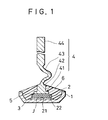
- Fig. 1 shows a typical embodiment of a semiconductor rectifying device of the present invention.
- one of the main surfaces 21 of a semiconductor chip 2 having a p-n junction J is bonded, via a bonding layer 3, to the bottom surface of a metallic container 1.
- the other main surface 22 of the semiconductor chip 2 is bonded via a bonding layer 5 to a header section 41 of a lead 4.
- the lead 4 is formed, in addition to the header section 41, a first lead section 42 extending vertically with respect to the header section 41, a flat curvature section 43 contiguous to the first lead section 42, and a second lead section 44 contiguous to the curvature section 43.
- the metallic container 1 is filled with a silicone resin layer 6 in which silica powder is added. This layer 6 covers the exposed section of the semiconductor chip 2 and the surface of the layer 6 reaches the first lead section 42.
- a silicone resin layer 6 in which silica powder is added.
- This layer 6 covers the exposed section of the semiconductor chip 2 and the surface of the layer 6 reaches the first lead section 42.
- copper, iron nickel alloys, or copper-iron nickel alloy clad materials may be used for a material of the metallic container 1.
- the surface of the container should preferably be covered with silver or nickel plating to prevent rust.
- a material formed into one piece of copper and whose surface is plated with silver or nickel to prevent rust should preferably be used for the lead 4.
- the header section 41 is made of molybdenum, tungsten, and an iron-nickel alloy.
- a certain material with the first lead section 42, the curvature section 43 and the second lead section 44, all of which are made of copper, bonded thereon may be used.
- Pb-Sn or Pb-Ag-Sn solder is used for the bonding layers 3 and 5.
- the silica powder added in the silicone resin layer 6 is highly pure silica whose content of Na and K is, respectively, 10 ppm or less.
- the silica powder has an average particle size of 2 to 6 /1.m.
- the amount of silica powder is in the range of 40 to 120 parts by weight with respect to 100 parts by weight of a silicone resin.
- the reason why highly pure silica is used is that if much Na and K is contained in the silica, a current which flows through a sealing resin layer, i.e., a reverse leak current, will be large when semiconductor rectifying devices are placed in a reverse bias state, thereby deteriorating the characteristics of the semiconductor rectifying devices. From this viewpoint, it is ideal that the content of the Na and K in the silica powder be 5 ppm or less. If the average particle size of the silica powder is too small, it becomes difficult to add an amount thereof sufficient for achieving the objects of the present invention to a silicone resin.
- the particle size range within which the objects of the present invention can be achieved is determined.
- an amount sufficient to prevent peeling at the bonding interface of the metallic container 1 from the silicone resin layer 6 is 40 parts by weight or greater, preferably 80 parts by weight or greater. If too much silica powder is added, the viscosity of the silicone resin will increase and thus a filling operation becomes difficult to perform, or it becomes difficult for air bubbles inside to escape. Thus, there are some cases in which it cannot be used as a sealing resin. Therefore, the amount of silica powder added is 120 parts by weight or less, preferably 100 parts by weight or less.
- a solder foil, the semiconductor chip 2, another solder foil, and the lead 4 are laminated on the bottom surface of the metallic container 1 and heated.
- a subassembly in which the metallic container 1, the semiconductor chip 2 and the lead 4 are made into one piece is formed.
- the metallic container 1 of this subassembly is filled with a liquid silicone resin which is prepared and purified so that 40 to 120 parts by weight of highly pure silica powder having an average particle size of 2 to 6 ⁇ m are contained therein with respect to 100 parts by weight of base oil compound comprising a dimethylpolysiloxane oil having vinyl groups bonded to silicon atom in its molecule, a methylhydrogenpolysiloxane having hydrogen atoms bonded to silicon atom in its molecule as a cross-linking agent, alkoxysilane type compound as a adhesive agent and a platinum type catalyst as main ingredients thereof.
- base oil compound comprising a dimethylpolysiloxane oil having vinyl groups bonded to silicon atom in its molecule, a methylhydrogenpolysiloxane having hydrogen atoms bonded to silicon atom in its molecule as a cross-linking agent, alkoxysilane type compound as a adhesive agent and a platinum type catalyst as main ingredients thereof.
- the liquid silicone resin is cured in a primary curing process in which it is heated at approximately 50 ° C for two hours or more in the atmosphere or N 2 gas atmosphere. Furthermore, the liquid silicone resin is cured in a secondary curing process to strengthen the bonding between the metallic container, the semiconductor chip and the lead, in which process it is heated at 150 to 200 ° C in the same atmosphere for two hours or more. Thus, the manufacturing of the semiconductor rectifying device is completed.
- the x mark in the results indicates that the number of cycles up to the time the sealing resin deteriorates is very small and that the sealing resin cannot be used in a place where salt damage is expected;
- the A mark in the results indicates that the number of cycles is small and that use of the sealing resin in a place where salt damage is expected should be avoided;
- the 0 mark in the results indicates that the number of cycles is large and that the sealing resin can be used in a place where salt damage is expected;
- the @ mark in the results indicates a sealing resin better than that indicated by the 0 mark.
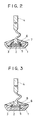
- Figs. 2 to 7 show different embodiments of a semiconductor rectifying device of the present invention.
- Fig. 2 shows an embodiment in which a polyimide resin layer 7 is interposed between the silicone resin layer 6 and the bottom surface of the metallic container 1, and between the semiconductor chip 2 and the header section 41 of the lead 4.
- Fig. 3 shows an embodiment in which an epoxy resin layer 8 is formed on the silicone resin layer 6.
- the other parts in Figs. 2 and 3 are the same as those in Fig. 1. All the parts shown in Figs. 2 and 3 are designed to increase the air-tight sealing function of a sealing resin.
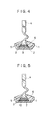
- Fig. 4 shows an embodiment in which a metallic plate 9 is disposed between the semiconductor chip 2 and the header section 41.
- Fig. 5 shows an embodiment in which a metallic plate 10 is disposed between the semiconductor chip 2 and the metallic container 1.
- metallic plates 9 and 10 are disposed to relieve thermal stress between the semiconductor chip 2 and the header section 41, and between the semiconductor chip 2 and the metallic container 1, respectively. Therefore, for example, molybdenum, tungsten, iron-nickel alloys, copper-iron nickel alloy-copper clad materials are used for metallic plates 9 and 10.
- Fig. 4 shows a case in which the metallic container 1 is of a material having a thermal expansion coefficient nearly equal to that of the semiconductor chip 2.
- Fig. 5 shows a case in which the header section 41 is of a material having a thermal expansion coefficient nearly equal to that of the semiconductor chip 2. If both the metallic container 1 and the header section 41 are copper, it is desirable that the metallic plates 9 and 10 be placed on both sides of the semiconductor chip 2.
- Fig. 6 shows an embodiment in which a knurling process 1 a is performed on the outer surface of the metallic container 1 in the same direction as that in which the lead 4 extends. This obviates a bonding operation when a full-wave rectifier is fabricated.
- Fig. 7 shows an embodiment in which a recessed section 11 a in a portion of the metallic container 1 is used in place of a metallic container.
- Figs. 8 and 9 show an embodiment of a full-wave rectifier in which semiconductor rectifying devices of the present invention are used.
- reference numerals 801 and 802 denote a first and second radiator, respectively, each of which is arc-shaped and has three recessed sections 801 a and 802a.
- the semiconductor chip 2 is bonded to the bottom surface of each recessed section of each radiator in the same manner as shown in Fig. 7.
- the lead 4 is bonded to the semiconductor chip 2.
- the recessed sections are filled with the silicone resin layer 6 containing silica powder sufficient to cover the semiconductor chip 2.
- the first and second semiconductor rectifying devices are formed.
- a p layer is positioned on the bottom surface thereof.
- Reference numeral 803 denotes an insulating member whose ring-like portion is open, which is fixedly mounted on the arc-shaped outer edge of the first and second radiators 801 and 802 by means of a screw 804. Thus, the positional relationship between the first and second radiators 801 and 802 is maintained constant.
- Reference numerals 805 and 806 respectively denote first and second long-piece lead terminals fastened at predetermined intervals on the insulating member 803 by a rivet 807. They are disposed at positions corresponding to the recessed sections 801 a and 802a of the radiators 801 and 802, respectively.
- the longitudinal direction of the long-piece lead terminals 805 and 806 is made in the same direction as the radial direction of a circle made by the insulating member 803, and notches 805a and 806a are disposed on both ends thereof.
- One of the ends (the internal end) of the first long-piece lead terminal 805 is soldered at the notch 805a with the lead of the first semiconductor rectifying device formed in the first radiator 801.
- One of the ends (the internal end) of the second long-piece lead terminal 806 is soldered at the notch 806a with the lead of the second semiconductor rectifying device formed in the second radiator 802.
- first and second long-piece lead terminals 805 and 806 are connected to each other by first, second and third terminals 808, 809 and 810.
- a three-phase full-wave rectifier is formed as described above with the first and second radiators 801 and 802 as D.C. terminals and the first, second and third terminals as A.C. terminals.
- This full-wave rectifier is used in a state in which it is fixedly mounted on the exterior of an A.C. generator inside an engine chamber of a vehicle.
- the sealing resin is exposed to the outside air even when it is fabricated in a full-wave rectifier. Hence, resistance to salt damage is still required. Therefore, the present invention is applicable to a full-wave rectifier.
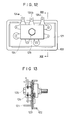
- Figs. 10 and 11 show another embodiment of a full-wave rectifier of the present invention. Points of difference between Figs. 10 and 11 and Figs. 8 and 9 are that semiconductor rectifying devices have been constructed as shown in Fig. 6 and they are press-fitted into through holes 101 a and 102a formed in a first and second radiator 101 and 102; and that portions of the first radiator 101 and the second radiator 102 are stacked in part on one another via an insulation spacer 103.
- Reference numeral 104 denotes a resinous terminal base, disposed on the first radiator 101, for holding A.C. terminals 104a, 104b and 104c in one piece.
- Reference numeral 105 denotes a fastening bolt for fixedly mounting the first radiator 101 and the second radiator 102 together.
- FIGs. 10 and 11 four semiconductor rectifying devices are mounted on each of the radiators. Three of them are used for rectification, and the remaining one is used as a neutral- point diode. Since this is not directly related to the present invention, an explanation thereof is omitted. The advantages of this embodiment are the same as those of the embodiment of Figs. 8 and 9.
- Figs. 12 and 13 show a further embodiment of a full-wave rectifier of the present invention. Points of difference between Figs. 12 and 13 and Figs. 8 and 9 are that a first radiator 121 and a second radiator 122 are shaped rectangularly and the first radiator 121 and the second radiator 122 are almost completely stacked flush to each other via an insulating spacer 123.
- Reference numeral 124 denotes a resinous terminal base, disposed on the first radiator 121, for holding A.C. terminals 124a, 124b and 124c in one piece.
- Reference numeral 125 denotes a fastening bolt for fixedly mounting the the first radiator 121 and the second radiator 122 together. This embodiment also has the same advantages as those of the embodiment of Figs. 8 and 9.
- a silicone resin containing silica powder is used as a sealing resin, according to the present invention, it is possible to realize a semiconductor rectifying device having excellent resistance to salt damage and suitable for installation in vehicles and a full-wave rectifier fabricated by using the same device.
Landscapes
- Engineering & Computer Science (AREA)
- Power Engineering (AREA)
- Structures Or Materials For Encapsulating Or Coating Semiconductor Devices Or Solid State Devices (AREA)
Applications Claiming Priority (2)
| Application Number | Priority Date | Filing Date | Title |
|---|---|---|---|
| JP270188/90 | 1990-10-08 | ||
| JP2270188A JP2858166B2 (ja) | 1990-10-08 | 1990-10-08 | 半導体整流素子及びそれを使った全波整流装置 |
Publications (2)
| Publication Number | Publication Date |
|---|---|
| EP0480372A1 true EP0480372A1 (fr) | 1992-04-15 |
| EP0480372B1 EP0480372B1 (fr) | 1996-06-19 |
Family
ID=17482751
Family Applications (1)
| Application Number | Title | Priority Date | Filing Date |
|---|---|---|---|
| EP91117134A Expired - Lifetime EP0480372B1 (fr) | 1990-10-08 | 1991-10-08 | Dispositif redresseur semiconducteur et redresseur double alternance l'utilisant |
Country Status (5)
| Country | Link |
|---|---|
| US (1) | US5302856A (fr) |
| EP (1) | EP0480372B1 (fr) |
| JP (1) | JP2858166B2 (fr) |
| KR (1) | KR100193161B1 (fr) |
| DE (1) | DE69120366T2 (fr) |
Cited By (5)
| Publication number | Priority date | Publication date | Assignee | Title |
|---|---|---|---|---|
| FR2716047A1 (fr) * | 1994-02-09 | 1995-08-11 | Bosch Gmbh Robert | Système de redressement pour un alternateur triphasé dont les diodes de puissance sont constituées comme des diodes pastilles. |
| EP0757423A1 (fr) * | 1995-08-02 | 1997-02-05 | Valeo Equipements Electriques Moteur | Alternateur comportant des pièces d'adaptation pour diodes de pont redresseur, notamment pour véhicule automobile, et pièce d'adaptation pour un tel alternateur |
| EP0901167A1 (fr) * | 1997-09-08 | 1999-03-10 | Valeo Equipements Electriques Moteur | Embase pour diode de puissance d'alternateur de véhicule automobile |
| EP0812014A3 (fr) * | 1996-06-06 | 1999-09-22 | General Motors Corporation | Ensemble redresseur de puissance |
| WO2000001055A1 (fr) * | 1998-06-26 | 2000-01-06 | Robert Bosch Gmbh | Machine electrique, de preference generateur de courant triphase pourvu d'une unite redresseur |
Families Citing this family (10)
| Publication number | Priority date | Publication date | Assignee | Title |
|---|---|---|---|---|
| US6160309A (en) * | 1999-03-25 | 2000-12-12 | Le; Hiep | Press-fit semiconductor package |
| US6614108B1 (en) * | 2000-10-23 | 2003-09-02 | Delphi Technologies, Inc. | Electronic package and method therefor |
| JP2002359328A (ja) * | 2001-03-29 | 2002-12-13 | Hitachi Ltd | 半導体装置 |
| JP2007042900A (ja) * | 2005-08-04 | 2007-02-15 | Denso Corp | 半導体装置 |
| JP4875902B2 (ja) * | 2006-02-08 | 2012-02-15 | 株式会社日立製作所 | 半導体装置 |
| CN101424662B (zh) * | 2007-10-31 | 2011-06-08 | 鸿富锦精密工业(深圳)有限公司 | 超声波扫描仪 |
| CN101430305B (zh) * | 2007-11-06 | 2011-03-23 | 鸿富锦精密工业(深圳)有限公司 | 超声波扫描仪 |
| JP4961398B2 (ja) * | 2008-06-30 | 2012-06-27 | 株式会社日立製作所 | 半導体装置 |
| JP6641161B2 (ja) * | 2015-11-18 | 2020-02-05 | 株式会社 日立パワーデバイス | 半導体装置、およびそれを用いたオルタネータ |
| JP7842341B2 (ja) * | 2022-03-10 | 2026-04-08 | ミネベアパワーデバイス株式会社 | 半導体装置 |
Citations (3)
| Publication number | Priority date | Publication date | Assignee | Title |
|---|---|---|---|---|
| DE2632154A1 (de) * | 1975-07-18 | 1977-02-10 | Hitachi Ltd | Halbleiteranordnung mit einem an einem metallwaermeabstrahler angeloeteten halbleiterbauelement |
| DE2649429A1 (de) * | 1975-11-28 | 1977-06-08 | Nippon Denso Co | Gleichrichtervorrichtung |
| DE3527496A1 (de) * | 1984-09-05 | 1986-03-13 | Mitsubishi Denki K.K., Tokio/Tokyo | In kunststoff eingegossene halbleitereinrichtung |
Family Cites Families (10)
| Publication number | Priority date | Publication date | Assignee | Title |
|---|---|---|---|---|
| JPS542067A (en) * | 1977-06-07 | 1979-01-09 | Hitachi Ltd | Semiconductor device |
| JPS55125657A (en) * | 1979-03-20 | 1980-09-27 | Nippon Denso Co Ltd | Rectifier |
| JPS6040189B2 (ja) * | 1979-09-21 | 1985-09-10 | 株式会社日立製作所 | 樹脂封止型半導体装置 |
| JPS58147036A (ja) * | 1982-02-26 | 1983-09-01 | Hitachi Ltd | 半導体装置の製造方法 |
| JPS59172749A (ja) * | 1983-03-23 | 1984-09-29 | Toshiba Corp | 半導体整流素子 |
| US4720424A (en) * | 1984-06-18 | 1988-01-19 | Hoebbst Celanese Corporation | Electronic component encapsulated with a composition comprising a polymer which is capable of forming an anisotropic melt phase and substantially incapable of further chain growth upon heating |
| DE3442132A1 (de) * | 1984-11-17 | 1986-05-22 | Messerschmitt-Bölkow-Blohm GmbH, 8012 Ottobrunn | Verfahren zur verkapselung von mikroelektronikschaltungen mit organischen komponenten |
| US4888634A (en) * | 1987-07-24 | 1989-12-19 | Linear Technology Corporation | High thermal resistance bonding material and semiconductor structures using same |
| JP2712618B2 (ja) * | 1989-09-08 | 1998-02-16 | 三菱電機株式会社 | 樹脂封止型半導体装置 |
| US5005069A (en) * | 1990-04-30 | 1991-04-02 | Motorola Inc. | Rectifier and method |
-
1990
- 1990-10-08 JP JP2270188A patent/JP2858166B2/ja not_active Expired - Fee Related
-
1991
- 1991-10-08 US US07/772,871 patent/US5302856A/en not_active Expired - Lifetime
- 1991-10-08 EP EP91117134A patent/EP0480372B1/fr not_active Expired - Lifetime
- 1991-10-08 DE DE69120366T patent/DE69120366T2/de not_active Expired - Fee Related
- 1991-10-08 KR KR1019910017579A patent/KR100193161B1/ko not_active Expired - Fee Related
Patent Citations (3)
| Publication number | Priority date | Publication date | Assignee | Title |
|---|---|---|---|---|
| DE2632154A1 (de) * | 1975-07-18 | 1977-02-10 | Hitachi Ltd | Halbleiteranordnung mit einem an einem metallwaermeabstrahler angeloeteten halbleiterbauelement |
| DE2649429A1 (de) * | 1975-11-28 | 1977-06-08 | Nippon Denso Co | Gleichrichtervorrichtung |
| DE3527496A1 (de) * | 1984-09-05 | 1986-03-13 | Mitsubishi Denki K.K., Tokio/Tokyo | In kunststoff eingegossene halbleitereinrichtung |
Non-Patent Citations (4)
| Title |
|---|
| PATENT ABSTRACTS OF JAPAN, vol. 11, no. 104 (E-494)[2551], 2nd April 1987; & JP-A-61 253 841 (TOSHIBA) 11-11-1986 * |
| PATENT ABSTRACTS OF JAPAN, vol. 11, no. 307 (C-450)[2754], 7th October 1987; & JP-A-62 96 567 (DENKI KAGAKU) 06-05-1987 * |
| PATENT ABSTRACTS OF JAPAN, vol. 5, no. 129 (E-70)[801], 19th August 1981; & JP-A-56 66 062 (HITACHI) 04-06-1981 * |
| PATENT ABSTRACTS OF JAPAN, vol. 9, no. 27 (E-294)[1750], 6th February 1985; & JP-A-59 172 749 (TOSHIBA) 29-09-1984 * |
Cited By (11)
| Publication number | Priority date | Publication date | Assignee | Title |
|---|---|---|---|---|
| FR2716047A1 (fr) * | 1994-02-09 | 1995-08-11 | Bosch Gmbh Robert | Système de redressement pour un alternateur triphasé dont les diodes de puissance sont constituées comme des diodes pastilles. |
| US5691892A (en) * | 1994-02-09 | 1997-11-25 | Robert Bosch Gmbh | Rectifier arrangement for a three-phase generator |
| EP0757423A1 (fr) * | 1995-08-02 | 1997-02-05 | Valeo Equipements Electriques Moteur | Alternateur comportant des pièces d'adaptation pour diodes de pont redresseur, notamment pour véhicule automobile, et pièce d'adaptation pour un tel alternateur |
| FR2737618A1 (fr) * | 1995-08-02 | 1997-02-07 | Valeo Equip Electr Moteur | Alternateur comportant des pieces d'adaptation pour diodes de pont redresseur, notamment pour vehicule automobile, et piece d'adaptation pour un tel alternateur |
| US5982062A (en) * | 1995-08-02 | 1999-11-09 | Valeo Equipements Electriques Moteur | Alternator including adaptors for rectifier bridge diodes, in particular for a motor vehicle, and an adaptor for such an alternator |
| CN1066865C (zh) * | 1995-08-02 | 2001-06-06 | 瓦莱奥电机设备公司 | 交流发电机及其装备的接合器 |
| EP0812014A3 (fr) * | 1996-06-06 | 1999-09-22 | General Motors Corporation | Ensemble redresseur de puissance |
| EP0901167A1 (fr) * | 1997-09-08 | 1999-03-10 | Valeo Equipements Electriques Moteur | Embase pour diode de puissance d'alternateur de véhicule automobile |
| FR2768261A1 (fr) * | 1997-09-08 | 1999-03-12 | Valeo Equip Electr Moteur | Embase pour diode de puissance d'alternateur de vehicule automobile |
| WO2000001055A1 (fr) * | 1998-06-26 | 2000-01-06 | Robert Bosch Gmbh | Machine electrique, de preference generateur de courant triphase pourvu d'une unite redresseur |
| US6307289B1 (en) * | 1998-06-26 | 2001-10-23 | Robert Bosch Gmbh | Electrical machine with rectifier unit and plus and minus heat sinks with improved lost heat dissipation |
Also Published As
| Publication number | Publication date |
|---|---|
| KR920008789A (ko) | 1992-05-28 |
| KR100193161B1 (ko) | 1999-06-15 |
| US5302856A (en) | 1994-04-12 |
| DE69120366D1 (de) | 1996-07-25 |
| JP2858166B2 (ja) | 1999-02-17 |
| EP0480372B1 (fr) | 1996-06-19 |
| DE69120366T2 (de) | 1996-11-07 |
| JPH04146655A (ja) | 1992-05-20 |
Similar Documents
| Publication | Publication Date | Title |
|---|---|---|
| US5302856A (en) | Semiconductor rectifying device and full-wave rectifier fabricated using the same | |
| US5430330A (en) | Semiconductor device, resin for sealing same and method of fabricating same | |
| KR100589097B1 (ko) | 봉지용 에폭시수지 조성물 및 전자장치 | |
| EP0662244B1 (fr) | Boitier en plastique renfermant des semi-conducteurs a diffuseur de chaleur en aluminium | |
| EP0114917A2 (fr) | Empaquetages pour semi-conducteurs | |
| EP0211618B1 (fr) | Empaquetage pour circuit intégré | |
| US10256169B2 (en) | Semiconductor device | |
| US11462450B2 (en) | Semiconductor device | |
| WO1996002942A1 (fr) | Boitier pour semi-conducteur a diffuseur thermique | |
| WO2003007362A1 (fr) | Utilisation de divers materiaux dans un assemblage d'appareils electroniques contenant une cavite d'air | |
| EP4057335A1 (fr) | Boîtier à semi-conducteurs et son procédé de fabrication | |
| GB2034520A (en) | Semiconductor assembly | |
| CN102576704B (zh) | 半导体装置 | |
| JP7589576B2 (ja) | 回路基板の製造方法 | |
| KR102403966B1 (ko) | 고방열 igbt 전력 반도체 패키지 및 제조 방법 | |
| JPH07157537A (ja) | 半導体封止用エポキシ樹脂組成物 | |
| JP2001011290A (ja) | 封止用エポキシ樹脂成形材料及び電子部品装置 | |
| US20230282601A1 (en) | Semiconductor joining, semiconductor device | |
| Wada et al. | Analysis of Corrosion on Aluminum Double‐Layer Metallization | |
| JP3235798B2 (ja) | エポキシ樹脂組成物 | |
| JP2885289B2 (ja) | エポキシ樹脂組成物 | |
| JP2991846B2 (ja) | エポキシ樹脂組成物 | |
| JP3011807B2 (ja) | エポキシ樹脂組成物 | |
| JP3093051B2 (ja) | エポキシ樹脂組成物 | |
| JP2024000325A (ja) | 半導体装置 |
Legal Events
| Date | Code | Title | Description |
|---|---|---|---|
| PUAI | Public reference made under article 153(3) epc to a published international application that has entered the european phase |
Free format text: ORIGINAL CODE: 0009012 |
|
| AK | Designated contracting states |
Kind code of ref document: A1 Designated state(s): DE FR |
|
| 17P | Request for examination filed |
Effective date: 19921006 |
|
| 17Q | First examination report despatched |
Effective date: 19940408 |
|
| GRAH | Despatch of communication of intention to grant a patent |
Free format text: ORIGINAL CODE: EPIDOS IGRA |
|
| GRAH | Despatch of communication of intention to grant a patent |
Free format text: ORIGINAL CODE: EPIDOS IGRA |
|
| GRAA | (expected) grant |
Free format text: ORIGINAL CODE: 0009210 |
|
| AK | Designated contracting states |
Kind code of ref document: B1 Designated state(s): DE FR |
|
| REF | Corresponds to: |
Ref document number: 69120366 Country of ref document: DE Date of ref document: 19960725 |
|
| ET | Fr: translation filed | ||
| PLBE | No opposition filed within time limit |
Free format text: ORIGINAL CODE: 0009261 |
|
| STAA | Information on the status of an ep patent application or granted ep patent |
Free format text: STATUS: NO OPPOSITION FILED WITHIN TIME LIMIT |
|
| 26N | No opposition filed | ||
| PGFP | Annual fee paid to national office [announced via postgrant information from national office to epo] |
Ref country code: FR Payment date: 20080919 Year of fee payment: 18 |
|
| PGFP | Annual fee paid to national office [announced via postgrant information from national office to epo] |
Ref country code: DE Payment date: 20081031 Year of fee payment: 18 |
|
| REG | Reference to a national code |
Ref country code: FR Ref legal event code: ST Effective date: 20100630 |
|
| PG25 | Lapsed in a contracting state [announced via postgrant information from national office to epo] |
Ref country code: FR Free format text: LAPSE BECAUSE OF NON-PAYMENT OF DUE FEES Effective date: 20091102 Ref country code: DE Free format text: LAPSE BECAUSE OF NON-PAYMENT OF DUE FEES Effective date: 20100501 |