EP0480409A1 - Méthode de fabrication d'un contact Ti/TiN/Al comprenant une étape de pulvérisation réactive - Google Patents
Méthode de fabrication d'un contact Ti/TiN/Al comprenant une étape de pulvérisation réactive Download PDFInfo
- Publication number
- EP0480409A1 EP0480409A1 EP91117237A EP91117237A EP0480409A1 EP 0480409 A1 EP0480409 A1 EP 0480409A1 EP 91117237 A EP91117237 A EP 91117237A EP 91117237 A EP91117237 A EP 91117237A EP 0480409 A1 EP0480409 A1 EP 0480409A1
- Authority
- EP
- European Patent Office
- Prior art keywords
- titanium
- film
- nitride film
- titanium nitride
- orientation ratio
- Prior art date
- Legal status (The legal status is an assumption and is not a legal conclusion. Google has not performed a legal analysis and makes no representation as to the accuracy of the status listed.)
- Granted
Links
Images

Classifications
-
- H—ELECTRICITY
- H10—SEMICONDUCTOR DEVICES; ELECTRIC SOLID-STATE DEVICES NOT OTHERWISE PROVIDED FOR
- H10W—GENERIC PACKAGES, INTERCONNECTIONS, CONNECTORS OR OTHER CONSTRUCTIONAL DETAILS OF DEVICES COVERED BY CLASS H10
- H10W20/00—Interconnections in chips, wafers or substrates
- H10W20/01—Manufacture or treatment
- H10W20/031—Manufacture or treatment of conductive parts of the interconnections
- H10W20/032—Manufacture or treatment of conductive parts of the interconnections of conductive barrier, adhesion or liner layers
- H10W20/052—Manufacture or treatment of conductive parts of the interconnections of conductive barrier, adhesion or liner layers by treatments not introducing additional elements therein
- H10W20/0526—Manufacture or treatment of conductive parts of the interconnections of conductive barrier, adhesion or liner layers by treatments not introducing additional elements therein by thermal treatment thereof
-
- C—CHEMISTRY; METALLURGY
- C23—COATING METALLIC MATERIAL; COATING MATERIAL WITH METALLIC MATERIAL; CHEMICAL SURFACE TREATMENT; DIFFUSION TREATMENT OF METALLIC MATERIAL; COATING BY VACUUM EVAPORATION, BY SPUTTERING, BY ION IMPLANTATION OR BY CHEMICAL VAPOUR DEPOSITION, IN GENERAL; INHIBITING CORROSION OF METALLIC MATERIAL OR INCRUSTATION IN GENERAL
- C23C—COATING METALLIC MATERIAL; COATING MATERIAL WITH METALLIC MATERIAL; SURFACE TREATMENT OF METALLIC MATERIAL BY DIFFUSION INTO THE SURFACE, BY CHEMICAL CONVERSION OR SUBSTITUTION; COATING BY VACUUM EVAPORATION, BY SPUTTERING, BY ION IMPLANTATION OR BY CHEMICAL VAPOUR DEPOSITION, IN GENERAL
- C23C14/00—Coating by vacuum evaporation, by sputtering or by ion implantation of the coating forming material
- C23C14/06—Coating by vacuum evaporation, by sputtering or by ion implantation of the coating forming material characterised by the coating material
- C23C14/0641—Nitrides
-
- C—CHEMISTRY; METALLURGY
- C23—COATING METALLIC MATERIAL; COATING MATERIAL WITH METALLIC MATERIAL; CHEMICAL SURFACE TREATMENT; DIFFUSION TREATMENT OF METALLIC MATERIAL; COATING BY VACUUM EVAPORATION, BY SPUTTERING, BY ION IMPLANTATION OR BY CHEMICAL VAPOUR DEPOSITION, IN GENERAL; INHIBITING CORROSION OF METALLIC MATERIAL OR INCRUSTATION IN GENERAL
- C23C—COATING METALLIC MATERIAL; COATING MATERIAL WITH METALLIC MATERIAL; SURFACE TREATMENT OF METALLIC MATERIAL BY DIFFUSION INTO THE SURFACE, BY CHEMICAL CONVERSION OR SUBSTITUTION; COATING BY VACUUM EVAPORATION, BY SPUTTERING, BY ION IMPLANTATION OR BY CHEMICAL VAPOUR DEPOSITION, IN GENERAL
- C23C14/00—Coating by vacuum evaporation, by sputtering or by ion implantation of the coating forming material
- C23C14/22—Coating by vacuum evaporation, by sputtering or by ion implantation of the coating forming material characterised by the process of coating
- C23C14/34—Sputtering
- C23C14/3407—Cathode assembly for sputtering apparatus, e.g. Target
- C23C14/3414—Metallurgical or chemical aspects of target preparation, e.g. casting, powder metallurgy
-
- H—ELECTRICITY
- H10—SEMICONDUCTOR DEVICES; ELECTRIC SOLID-STATE DEVICES NOT OTHERWISE PROVIDED FOR
- H10P—GENERIC PROCESSES OR APPARATUS FOR THE MANUFACTURE OR TREATMENT OF DEVICES COVERED BY CLASS H10
- H10P14/00—Formation of materials, e.g. in the shape of layers or pillars
- H10P14/40—Formation of materials, e.g. in the shape of layers or pillars of conductive or resistive materials
- H10P14/42—Formation of materials, e.g. in the shape of layers or pillars of conductive or resistive materials using a gas or vapour
- H10P14/44—Physical vapour deposition [PVD]
-
- H—ELECTRICITY
- H10—SEMICONDUCTOR DEVICES; ELECTRIC SOLID-STATE DEVICES NOT OTHERWISE PROVIDED FOR
- H10W—GENERIC PACKAGES, INTERCONNECTIONS, CONNECTORS OR OTHER CONSTRUCTIONAL DETAILS OF DEVICES COVERED BY CLASS H10
- H10W20/00—Interconnections in chips, wafers or substrates
- H10W20/01—Manufacture or treatment
- H10W20/031—Manufacture or treatment of conductive parts of the interconnections
- H10W20/032—Manufacture or treatment of conductive parts of the interconnections of conductive barrier, adhesion or liner layers
- H10W20/033—Manufacture or treatment of conductive parts of the interconnections of conductive barrier, adhesion or liner layers in openings in dielectrics
-
- H—ELECTRICITY
- H10—SEMICONDUCTOR DEVICES; ELECTRIC SOLID-STATE DEVICES NOT OTHERWISE PROVIDED FOR
- H10W—GENERIC PACKAGES, INTERCONNECTIONS, CONNECTORS OR OTHER CONSTRUCTIONAL DETAILS OF DEVICES COVERED BY CLASS H10
- H10W20/00—Interconnections in chips, wafers or substrates
- H10W20/40—Interconnections external to wafers or substrates, e.g. back-end-of-line [BEOL] metallisations or vias connecting to gate electrodes
- H10W20/41—Interconnections external to wafers or substrates, e.g. back-end-of-line [BEOL] metallisations or vias connecting to gate electrodes characterised by their conductive parts
- H10W20/425—Barrier, adhesion or liner layers
-
- Y—GENERAL TAGGING OF NEW TECHNOLOGICAL DEVELOPMENTS; GENERAL TAGGING OF CROSS-SECTIONAL TECHNOLOGIES SPANNING OVER SEVERAL SECTIONS OF THE IPC; TECHNICAL SUBJECTS COVERED BY FORMER USPC CROSS-REFERENCE ART COLLECTIONS [XRACs] AND DIGESTS
- Y10—TECHNICAL SUBJECTS COVERED BY FORMER USPC
- Y10S—TECHNICAL SUBJECTS COVERED BY FORMER USPC CROSS-REFERENCE ART COLLECTIONS [XRACs] AND DIGESTS
- Y10S148/00—Metal treatment
- Y10S148/158—Sputtering
Definitions
- the present invention relates to a method of fabricating a semiconductor device and, particularly, to a method of forming an electrode wiring on a silicon substrate through a barrier metal.
- aluminum (Al) or an alloy thereof has been mainly used as material for forming electrode wirings which are in ohmic contact with respective impurity diffusion regions formed in a silicon (Si) substrate and further with the silicon substrate itself.
- Si silicon
- alloy spike and/or silicon nodule may be produced by reaction between aluminum and silicon due to thermal hysteresis of the metal deposition step and subsequent steps.
- breakage of wiring due to electromigration and/or stressmigration becomes severe problem.
- barrier metal layer between the silicon substrate and the metal layer forming the electrode wiring.
- a multi-layer wiring using such barrier metal layer is effective in preventing such wiring breakage due to electromigration or stressmigration.
- the barrier metal layer is generally formed only on the contact regions of the impurity diffusion regions to the electrodes. In order to improve the durability against stressmigration, however, it is popular recently that the barrier metal layer is formed not only on the contact regions but also on a wiring formation regions beneath the electrode wirings. The latter scheme is becoming popular.
- a titanium (Ti) film or a titanium nitride (TiN) film is mainly used as the barrier metal to be formed beneath the electrode wiring.
- an interlayer insulating film of such as silicon dioxide is formed on a silicon substrate in which desired diffusion regions are formed through desired impurity diffusion steps.
- a titanium (Ti) film and a titanium nitride (TiN) film are formed sequentially on the surface of the silicon substrate as a barrier metal, followed by carrying out heat treatment.
- An aluminum (Al) film is thereafter formed on the barrier metal layer, and these three metal layers are then patterned to form a three-layer electrode wiring.
- the titanium nitride film as the barrier metal is usually formed by reactive sputtering with using titanium as a target electrode in a mixture gas of argon (Ar) and nitrogen gas (N 2 ) as sputtering atmosphere.
- the subsequent heat treatment is performed by lamp annealing within nitrogen gas or NH 3 gas.
- the titanium film within the contact hole is silicided from the side of the silicon substrate while non-reacted titanium of the titanium nitride film and the titanium file are nitrided from the side of the sputtering gas. Therefore, the performance of the titanium film and the titanium nitride film as the barrier metal is improved and the contact resistance is reduced.
- This heat treatment was reported by H. Joswig and W. Pamler in June 12-13, 1990, VMIC Conference.
- the titanium nitride film is lamp-annealed to improve the properties thereof, it is crystallized by rapid heating and shrinked, resulting in fine cracks in the titanium nitride film. Therefore, the barrier performance of the titanium nitride film is degraded and leakage current is increased, resulting in degradation of reliability of the semiconductor device.
- An object of the present invention is to provide a method of fabricating semiconductor device, by which formation of fine cracks in a titanium nitride film during lamb-annealing is restricted and the reliability of resultant semiconductor device is improved.
- the present invention resides in that the titanium nitride film is formed by reactive sputtering with using a titanium target whose ratio of (001) plane among orientations existing a surface thereof, that is, orientation ratio, is not more than 70 %.
- the present inventors have found that, with the titanium target whose orientation ratio of (001) plane is not more than 70 %, the deposition rate of the titanium nitride film is reduced and residual oxygen in atmosphere is taken in the titanium nitride film thus formed.
- the titanium nitride film containing such large amount of oxygen does not rapidly shrink by lamp annealing. Since, therefore, the formation of fine cracks in the titanium nitride film is restricted, the degradation of barrier performance is avoided.
- the present invention is based on this discovery.
- Fig. 1 is a cross section of a semiconductor chip according to a first embodiment of the present invention
- an interlayer insulating film 2 of such as silicon dioxide (Si0 2 ) or PSG is formed on a silicon substrate 1 and then a contact hole 7 is formed by patterning the interlayer insulating film 2 thus formed.
- an impurity diffusion layer 3 is formed in a portion of the silicon substrate 1 corresponding to the contact hole 7 by introducing an impurity thereto.
- a titanium film 4 having thickness of 20 to 80 nm is deposited thereon by sputtering.
- the above-mentioned steps are the same as those used in the conventional fabrication method.
- a titanium nitride film 5 having thickness of 80 to 150 nm is deposited thereon by means of reactive sputtering using titanium as target.
- the titanium target to be used in this sputtering is preliminarily regulated such that its orientation ratio of (001) plane is about 50 %.
- the sputtering conditions are a mixture gas of argon (Ar) and nitrogen gas as sputtering atmosphere, total gas pressure of 4 mm Torr, power of 3 kW and substrate temperature of 200 ° C.
- a heat treatment is performed by a lamp annealing in nitriding atmosphere such as nitrogen gas or NH 3 gas at 500 to 900 C for 30 seconds.
- an aluminum film 6 is formed thereon and an electrode wiring having three-layer structure is formed by patterning the aluminum film 6, the titanium nitride film 5 and the titanium film 4, all together.
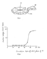
- the orientation ratio of (001) plane in a surface of a bulk titanium material 8 for ordinary titanium target was measured by such as X ray diffraction. Then, for example, titanium target plates 9A each having minimum orientation ratio were cut out in parallel to an X-Y plane and titanium target plates 9B each having maximum orientation ratio were cut out in parallel to a Y-Z plane. Then, as shown in Fig. 3, these plates 9A and 9B were cut to triangle shapes and arranged regularly to obtain a polygonal titanium target plate 10 whose combined orientation ratio of (001) plane is about 50 %.
- a surface of a titanium target in nitriding atmosphere is converted by reaction with nitrogen in plasma into titanium nitride and the latter is sputtered.
- the orientation ratio of (001) plane of the titanium target surface is high, an amount of titanium nitride sputtered from the surface is increased and deposition rate of titanium nitride film on the silicon substrate is increased.
- the deposition rate of titanium nitride film is reduced and more residual oxygen in the atmosphere is taken in the titanium nitride film.
- the titanium target plates are cut out from the bulk material after the orientation ratio of (001) plane thereof is measured, it is possible to produce a titanium target having orientation ratio of (001) plane of not more than 70 %, by cutting target plates from a titanium bulk material in parallel to three or more directions and regularly arranging them.
- the shape of the titanium target is not limited to octagonal as shown in Fig. 3 and any other polygonal shape or even circular shape may be possible.
- a second embodiment of the present invention will be described.
- the step of forming a titanium nitride film by using a titanium target whose orientation ratio of (001) plane is not more than 70 % is the same as in the first embodiment
- the orientation ratio in the second embodiment is regulated to not more than 70 % by means of annealing.
- the titanium target is prepared by cutting and shaping a bulk titanium material.
- the titanium bulk material is annealed at 600 to 1600°C.
- titanium in the bulk material recrystallized and grain growth speed is higher with higher temperature and longer treating time, resulting in higher orientation ratio of (001) plane of the titanium target surface. Therefore, when a surface of the annealed bulk material is used as a surface of the titanium target, the orientation ratio of (001) plane of the target may become larger than 70 %, causing junction leakage defect to be increased.
- the titanium target in the second embodiment was prepared by annealing the bulk material at 1000 to 1600°C for 5 to 30 minutes.
- the orientation ratio of (001) plane of the titanium bulk material annealed at 1100 ° C for 10 minutes was 30 to 40 %.
- the junction leak defect was as small as in the first embodiment, improving the reliability of the semiconductor device.
Landscapes
- Chemical & Material Sciences (AREA)
- Chemical Kinetics & Catalysis (AREA)
- Engineering & Computer Science (AREA)
- Materials Engineering (AREA)
- Mechanical Engineering (AREA)
- Metallurgy (AREA)
- Organic Chemistry (AREA)
- Internal Circuitry In Semiconductor Integrated Circuit Devices (AREA)
- Electrodes Of Semiconductors (AREA)
Applications Claiming Priority (2)
| Application Number | Priority Date | Filing Date | Title |
|---|---|---|---|
| JP271042/90 | 1990-10-09 | ||
| JP27104290 | 1990-10-09 |
Publications (2)
| Publication Number | Publication Date |
|---|---|
| EP0480409A1 true EP0480409A1 (fr) | 1992-04-15 |
| EP0480409B1 EP0480409B1 (fr) | 1994-07-13 |
Family
ID=17494595
Family Applications (1)
| Application Number | Title | Priority Date | Filing Date |
|---|---|---|---|
| EP91117237A Expired - Lifetime EP0480409B1 (fr) | 1990-10-09 | 1991-10-09 | Méthode de fabrication d'un contact Ti/TiN/Al comprenant une étape de pulvérisation réactive |
Country Status (4)
| Country | Link |
|---|---|
| US (1) | US5155063A (fr) |
| EP (1) | EP0480409B1 (fr) |
| KR (1) | KR950009278B1 (fr) |
| DE (1) | DE69102851T2 (fr) |
Cited By (6)
| Publication number | Priority date | Publication date | Assignee | Title |
|---|---|---|---|---|
| EP0697729A3 (fr) * | 1994-08-18 | 1996-11-13 | Oki Electric Ind Co Ltd | Structure de contact avec un métal de barrage et procédé de fabrication |
| EP0717436A3 (fr) * | 1994-12-15 | 1997-03-05 | Motorola Inc | Procédé de fabrication d'une couche métallique orientée et d'une structure de contact d'un composant semi-conducteur |
| EP0785292A1 (fr) * | 1993-09-27 | 1997-07-23 | Japan Energy Corporation | Cible de pulvérisation en titane de haute pureté |
| US6031290A (en) * | 1992-12-09 | 2000-02-29 | Semiconductor Energy Laboratory Co., Ltd. | Electronic circuit |
| EP1022352A3 (fr) * | 1998-12-28 | 2002-01-02 | Infineon Technologies North America Corp. | Méthode de fabrication d'interconnections métalliques, avec une durée de vie élevée en regard de l'électromigration |
| WO2004066384A1 (fr) * | 2003-01-23 | 2004-08-05 | Fraunhofer Ges Forschung | Structure de circuit programmable et procede pour la produire |
Families Citing this family (19)
| Publication number | Priority date | Publication date | Assignee | Title |
|---|---|---|---|---|
| AU8519891A (en) * | 1990-08-01 | 1992-03-02 | Staktek Corporation | Ultra high density integrated circuit packages, method and apparatus |
| US5377077A (en) * | 1990-08-01 | 1994-12-27 | Staktek Corporation | Ultra high density integrated circuit packages method and apparatus |
| US5446620A (en) * | 1990-08-01 | 1995-08-29 | Staktek Corporation | Ultra high density integrated circuit packages |
| US5858868A (en) * | 1992-05-08 | 1999-01-12 | Yamaha Corporation | Method of manufacturing a laminated wiring structure preventing impurity diffusion therein from N+ and P+ regions in CMOS device with ohmic contact |
| US5369056A (en) * | 1993-03-29 | 1994-11-29 | Staktek Corporation | Warp-resistent ultra-thin integrated circuit package fabrication method |
| US5801437A (en) * | 1993-03-29 | 1998-09-01 | Staktek Corporation | Three-dimensional warp-resistant integrated circuit module method and apparatus |
| US5358615A (en) * | 1993-10-04 | 1994-10-25 | Motorola, Inc. | Process for forming a sputter deposited metal film |
| US5705429A (en) * | 1993-10-04 | 1998-01-06 | Yamaha Corporation | Method of manufacturing aluminum wiring at a substrate temperature from 100 to 150 degrees celsius |
| EP0690503A1 (fr) * | 1994-05-31 | 1996-01-03 | Advanced Micro Devices, Inc. | Structure améliorée d'une ligne d'interconnexion et procédé |
| JPH08176823A (ja) * | 1994-12-26 | 1996-07-09 | Sony Corp | 高融点金属薄膜の成膜方法 |
| JP2689931B2 (ja) * | 1994-12-29 | 1997-12-10 | 日本電気株式会社 | スパッタ方法 |
| JP2754176B2 (ja) * | 1995-03-13 | 1998-05-20 | エルジイ・セミコン・カンパニイ・リミテッド | 緻密なチタン窒化膜及び緻密なチタン窒化膜/薄膜のチタンシリサイドの形成方法及びこれを用いた半導体素子の製造方法 |
| TW290731B (fr) * | 1995-03-30 | 1996-11-11 | Siemens Ag | |
| US5776831A (en) * | 1995-12-27 | 1998-07-07 | Lsi Logic Corporation | Method of forming a high electromigration resistant metallization system |
| US5919342A (en) * | 1997-02-26 | 1999-07-06 | Applied Materials, Inc. | Method for depositing golden titanium nitride |
| KR100241506B1 (ko) * | 1997-06-23 | 2000-03-02 | 김영환 | 반도체 소자의 금속 배선 형성 방법 |
| US7550066B2 (en) * | 2004-07-09 | 2009-06-23 | Applied Materials, Inc. | Staggered target tiles |
| KR100714269B1 (ko) * | 2004-10-14 | 2007-05-02 | 삼성전자주식회사 | 반도체 소자 제조에 사용되는 금속층 형성방법 |
| JP5747091B2 (ja) * | 2012-01-12 | 2015-07-08 | Jx日鉱日石金属株式会社 | 高純度銅スパッタリングターゲット |
Citations (2)
| Publication number | Priority date | Publication date | Assignee | Title |
|---|---|---|---|---|
| FR2443926A1 (fr) * | 1978-12-13 | 1980-07-11 | Glyco Metall Werke | Materiau stratifie de glissement ou de frottement et procede pour sa fabrication |
| EP0310108A2 (fr) * | 1987-10-02 | 1989-04-05 | Kabushiki Kaisha Toshiba | Structure d'interconnexion d'un dispositif à semi-conducteur et son procédé de fabrication |
Family Cites Families (12)
| Publication number | Priority date | Publication date | Assignee | Title |
|---|---|---|---|---|
| JPS58101454A (ja) * | 1981-12-12 | 1983-06-16 | Nippon Telegr & Teleph Corp <Ntt> | 半導体装置の電極 |
| JPS6066425A (ja) * | 1983-09-22 | 1985-04-16 | Nippon Telegr & Teleph Corp <Ntt> | Lsi電極用の高純度モリブデンタ−ゲツトならびに高純度モリブデンシリサイドタ−ゲツトおよびその製造方法 |
| AT383758B (de) * | 1985-12-23 | 1987-08-25 | Plansee Metallwerk | Verfahren zur herstellung eines sputter-targets |
| JPS62284069A (ja) * | 1986-06-02 | 1987-12-09 | Sumitomo Special Metals Co Ltd | スパッタリング用タ−ゲット |
| JPS63111666A (ja) * | 1986-10-30 | 1988-05-16 | Mitsubishi Electric Corp | 半導体装置 |
| JPS63161163A (ja) * | 1986-12-25 | 1988-07-04 | Toshiba Corp | スパツタタ−ゲツトの固定治具 |
| US4960732A (en) * | 1987-02-19 | 1990-10-02 | Advanced Micro Devices, Inc. | Contact plug and interconnect employing a barrier lining and a backfilled conductor material |
| GB2208390B (en) * | 1987-08-06 | 1991-03-27 | Plessey Co Plc | Thin film deposition process |
| DE3731621A1 (de) * | 1987-09-19 | 1989-03-30 | Texas Instruments Deutschland | Verfahren zum herstellen einer elektrisch programmierbaren integrierten schaltung |
| JP2776826B2 (ja) * | 1988-04-15 | 1998-07-16 | 株式会社日立製作所 | 半導体装置およびその製造方法 |
| JP2671397B2 (ja) * | 1988-07-01 | 1997-10-29 | 住友化学工業株式会社 | マグネトロンスパッタリング用ターゲット |
| US4829024A (en) * | 1988-09-02 | 1989-05-09 | Motorola, Inc. | Method of forming layered polysilicon filled contact by doping sensitive endpoint etching |
-
1991
- 1991-10-09 KR KR1019910017666A patent/KR950009278B1/ko not_active Expired - Fee Related
- 1991-10-09 US US07/773,420 patent/US5155063A/en not_active Expired - Lifetime
- 1991-10-09 DE DE69102851T patent/DE69102851T2/de not_active Expired - Fee Related
- 1991-10-09 EP EP91117237A patent/EP0480409B1/fr not_active Expired - Lifetime
Patent Citations (2)
| Publication number | Priority date | Publication date | Assignee | Title |
|---|---|---|---|---|
| FR2443926A1 (fr) * | 1978-12-13 | 1980-07-11 | Glyco Metall Werke | Materiau stratifie de glissement ou de frottement et procede pour sa fabrication |
| EP0310108A2 (fr) * | 1987-10-02 | 1989-04-05 | Kabushiki Kaisha Toshiba | Structure d'interconnexion d'un dispositif à semi-conducteur et son procédé de fabrication |
Non-Patent Citations (6)
| Title |
|---|
| PATENT ABSTRACTS OF JAPAN vol. 12, no. 176 (C-498) 25 May 1988, & JP-A-62 284069 (SUMITOMO SPECIAL METALS CO. LTD.) 09 December 1987, * |
| PATENT ABSTRACTS OF JAPAN vol. 12, no. 357 (E-662) 26 September 1988, & JP-A-63 111666 (MITSUBISHI ELECTRIC CORP.) 15 June 1988, * |
| PATENT ABSTRACTS OF JAPAN vol. 12, no. 433 (C-543) 15 November 1988, & JP-A-63 161163 (TOSHIBA CORP.) 04 July 1988, * |
| PATENT ABSTRACTS OF JAPAN vol. 14, no. 146 (C-704) 20 March 1990, & JP-A-02 015167 (SUMITOMO CHEM.CO.LTD.) 18 January 1990, * |
| PATENT ABSTRACTS OF JAPAN vol. 7, no. 204 (E-197) 09 September 1983, & JP-A-58 101454 (NIPPON DENSHIN DENWA KOSHA) 16 June 1983, * |
| PROCEEDINGS 3RD. INTERNAT.IEEE VLSI MULTILEVEL INTERCONNECTION CONFERENCE 09 June 1986, SANTA CLARA, CA. pages 411 - 417; T. MAEDA et al.: "Ti thickness optimization of TiN/Ti barrier metal structure based upon BF2+ induced damage analysis" * |
Cited By (20)
| Publication number | Priority date | Publication date | Assignee | Title |
|---|---|---|---|---|
| US7061016B2 (en) | 1992-12-09 | 2006-06-13 | Semiconductor Energy Laboratory Co., Ltd. | Electronic circuit |
| US7897972B2 (en) | 1992-12-09 | 2011-03-01 | Semiconductor Energy Laboratory Co., Ltd. | Electronic circuit |
| US7105898B2 (en) | 1992-12-09 | 2006-09-12 | Semiconductor Energy Laboratory Co., Ltd. | Electronic circuit |
| US7045399B2 (en) | 1992-12-09 | 2006-05-16 | Semiconductor Energy Laboratory Co., Ltd. | Electronic circuit |
| US7547916B2 (en) | 1992-12-09 | 2009-06-16 | Semiconductor Energy Laboratory Co., Ltd. | Electronic circuit |
| US6448612B1 (en) | 1992-12-09 | 2002-09-10 | Semiconductor Energy Laboratory Co., Ltd. | Pixel thin film transistor and a driver circuit for driving the pixel thin film transistor |
| CN1111902C (zh) * | 1992-12-09 | 2003-06-18 | 株式会社半导体能源研究所 | 具有含铝互连线的半导体器件 |
| US6031290A (en) * | 1992-12-09 | 2000-02-29 | Semiconductor Energy Laboratory Co., Ltd. | Electronic circuit |
| US8294152B2 (en) | 1992-12-09 | 2012-10-23 | Semiconductor Energy Laboratory Co., Ltd. | Electronic circuit including pixel electrode comprising conductive film |
| US6166414A (en) * | 1992-12-09 | 2000-12-26 | Semiconductor Energy Laboratory Co., Ltd. | Electronic circuit |
| US6608353B2 (en) | 1992-12-09 | 2003-08-19 | Semiconductor Energy Laboratory Co., Ltd. | Thin film transistor having pixel electrode connected to a laminate structure |
| US5772860A (en) * | 1993-09-27 | 1998-06-30 | Japan Energy Corporation | High purity titanium sputtering targets |
| EP0785293A1 (fr) * | 1993-09-27 | 1997-07-23 | Japan Energy Corporation | Cible de pulvérisation en titane de haute pureté |
| EP0785292A1 (fr) * | 1993-09-27 | 1997-07-23 | Japan Energy Corporation | Cible de pulvérisation en titane de haute pureté |
| US5920122A (en) * | 1994-08-18 | 1999-07-06 | Oki Electric Industry Co., Ltd. | Contact structure using barrier metal and method of manufacturing the same |
| US5654235A (en) * | 1994-08-18 | 1997-08-05 | Oki Electric Industry Co., Ltd. | Method of manufacturing contact structure using barrier metal |
| EP0697729A3 (fr) * | 1994-08-18 | 1996-11-13 | Oki Electric Ind Co Ltd | Structure de contact avec un métal de barrage et procédé de fabrication |
| EP0717436A3 (fr) * | 1994-12-15 | 1997-03-05 | Motorola Inc | Procédé de fabrication d'une couche métallique orientée et d'une structure de contact d'un composant semi-conducteur |
| EP1022352A3 (fr) * | 1998-12-28 | 2002-01-02 | Infineon Technologies North America Corp. | Méthode de fabrication d'interconnections métalliques, avec une durée de vie élevée en regard de l'électromigration |
| WO2004066384A1 (fr) * | 2003-01-23 | 2004-08-05 | Fraunhofer Ges Forschung | Structure de circuit programmable et procede pour la produire |
Also Published As
| Publication number | Publication date |
|---|---|
| US5155063A (en) | 1992-10-13 |
| EP0480409B1 (fr) | 1994-07-13 |
| DE69102851D1 (de) | 1994-08-18 |
| DE69102851T2 (de) | 1995-02-16 |
| KR920008849A (ko) | 1992-05-28 |
| KR950009278B1 (ko) | 1995-08-18 |
Similar Documents
| Publication | Publication Date | Title |
|---|---|---|
| US5155063A (en) | Method of fabricating semiconductor device including an al/tin/ti contact | |
| EP0697729B1 (fr) | Structure de contact avec un métal de barrage et procédé de fabrication | |
| EP0735586B1 (fr) | Structures semi-conductrices | |
| US5162262A (en) | Multi-layered interconnection structure for a semiconductor device and manufactured method thereof | |
| JP2537413B2 (ja) | 半導体装置およびその製造方法 | |
| KR940010520B1 (ko) | 반도체장치 및 그 제조방법 | |
| US4937652A (en) | Semiconductor device and method of manufacturing the same | |
| US6329284B2 (en) | Manufacturing process of a semiconductor device | |
| US6410986B1 (en) | Multi-layered titanium nitride barrier structure | |
| JP3122845B2 (ja) | 半導体装置の金属配線形成方法 | |
| KR100205301B1 (ko) | 금속배선구조 및 형성방법 | |
| US5528081A (en) | High temperature refractory metal contact in silicon integrated circuits | |
| US7135399B2 (en) | Deposition method for wiring thin film | |
| KR930001311A (ko) | 반도체 장치의 금속 배선층 형성방법 | |
| JP3109091B2 (ja) | 半導体装置の製造方法 | |
| JP2737470B2 (ja) | 半導体装置の製造方法 | |
| JP2554634B2 (ja) | 半導体装置の製造方法 | |
| JPH04196122A (ja) | 半導体装置の製造方法 | |
| JPH06140401A (ja) | 集積回路装置 | |
| CN1606803A (zh) | 制造电子器件的方法 | |
| EP0225224A2 (fr) | Dépôt d'un oxyde après un procédé de formation d'un alliage métallique | |
| JPH0799193A (ja) | 半導体装置の製造方法 | |
| JP2711530B2 (ja) | 半導体素子の金属配線形成方法 | |
| US20050181600A1 (en) | Method of forming a semiconductor device having a Ti/TiN/Ti<002>/a1<111> laminate | |
| KR100217544B1 (ko) | 단계적 피복성이 우수한 배선 형성법 |
Legal Events
| Date | Code | Title | Description |
|---|---|---|---|
| PUAI | Public reference made under article 153(3) epc to a published international application that has entered the european phase |
Free format text: ORIGINAL CODE: 0009012 |
|
| 17P | Request for examination filed |
Effective date: 19911009 |
|
| AK | Designated contracting states |
Kind code of ref document: A1 Designated state(s): DE FR GB |
|
| 17Q | First examination report despatched |
Effective date: 19930818 |
|
| GRAA | (expected) grant |
Free format text: ORIGINAL CODE: 0009210 |
|
| AK | Designated contracting states |
Kind code of ref document: B1 Designated state(s): DE FR GB |
|
| REF | Corresponds to: |
Ref document number: 69102851 Country of ref document: DE Date of ref document: 19940818 |
|
| ET | Fr: translation filed | ||
| PLBE | No opposition filed within time limit |
Free format text: ORIGINAL CODE: 0009261 |
|
| STAA | Information on the status of an ep patent application or granted ep patent |
Free format text: STATUS: NO OPPOSITION FILED WITHIN TIME LIMIT |
|
| 26N | No opposition filed | ||
| REG | Reference to a national code |
Ref country code: GB Ref legal event code: IF02 |
|
| REG | Reference to a national code |
Ref country code: GB Ref legal event code: 732E |
|
| REG | Reference to a national code |
Ref country code: FR Ref legal event code: TP |
|
| PGFP | Annual fee paid to national office [announced via postgrant information from national office to epo] |
Ref country code: FR Payment date: 20031003 Year of fee payment: 13 |
|
| PGFP | Annual fee paid to national office [announced via postgrant information from national office to epo] |
Ref country code: GB Payment date: 20031008 Year of fee payment: 13 |
|
| PGFP | Annual fee paid to national office [announced via postgrant information from national office to epo] |
Ref country code: DE Payment date: 20031016 Year of fee payment: 13 |
|
| PG25 | Lapsed in a contracting state [announced via postgrant information from national office to epo] |
Ref country code: GB Free format text: LAPSE BECAUSE OF NON-PAYMENT OF DUE FEES Effective date: 20041009 |
|
| PG25 | Lapsed in a contracting state [announced via postgrant information from national office to epo] |
Ref country code: DE Free format text: LAPSE BECAUSE OF NON-PAYMENT OF DUE FEES Effective date: 20050503 |
|
| GBPC | Gb: european patent ceased through non-payment of renewal fee |
Effective date: 20041009 |
|
| PG25 | Lapsed in a contracting state [announced via postgrant information from national office to epo] |
Ref country code: FR Free format text: LAPSE BECAUSE OF NON-PAYMENT OF DUE FEES Effective date: 20050630 |
|
| REG | Reference to a national code |
Ref country code: FR Ref legal event code: ST |