EP0480477B1 - Couplage entre une fibre optique et un élément optique à guide d'onde - Google Patents
Couplage entre une fibre optique et un élément optique à guide d'onde Download PDFInfo
- Publication number
- EP0480477B1 EP0480477B1 EP19910117665 EP91117665A EP0480477B1 EP 0480477 B1 EP0480477 B1 EP 0480477B1 EP 19910117665 EP19910117665 EP 19910117665 EP 91117665 A EP91117665 A EP 91117665A EP 0480477 B1 EP0480477 B1 EP 0480477B1
- Authority
- EP
- European Patent Office
- Prior art keywords
- waveguide
- optical
- slot
- optical fiber
- layer
- Prior art date
- Legal status (The legal status is an assumption and is not a legal conclusion. Google has not performed a legal analysis and makes no representation as to the accuracy of the status listed.)
- Expired - Lifetime
Links
- 230000003287 optical effect Effects 0.000 title claims description 75
- 239000013307 optical fiber Substances 0.000 title claims description 71
- 238000010168 coupling process Methods 0.000 title claims description 20
- 230000008878 coupling Effects 0.000 title claims description 17
- 238000005859 coupling reaction Methods 0.000 title claims description 17
- 239000007788 liquid Substances 0.000 claims description 42
- 239000000853 adhesive Substances 0.000 claims description 41
- 230000001070 adhesive effect Effects 0.000 claims description 41
- 239000000835 fiber Substances 0.000 claims description 32
- 238000000034 method Methods 0.000 claims description 31
- 230000010355 oscillation Effects 0.000 claims description 13
- 238000004806 packaging method and process Methods 0.000 claims description 13
- 238000000016 photochemical curing Methods 0.000 claims description 6
- 239000002318 adhesion promoter Substances 0.000 claims description 5
- 230000032798 delamination Effects 0.000 claims description 5
- BLRPTPMANUNPDV-UHFFFAOYSA-N Silane Chemical group [SiH4] BLRPTPMANUNPDV-UHFFFAOYSA-N 0.000 claims description 4
- 229910000077 silane Inorganic materials 0.000 claims description 4
- 239000010410 layer Substances 0.000 description 99
- 239000000178 monomer Substances 0.000 description 48
- 239000000203 mixture Substances 0.000 description 31
- 239000000872 buffer Substances 0.000 description 26
- 238000003780 insertion Methods 0.000 description 25
- 230000037431 insertion Effects 0.000 description 25
- 239000000463 material Substances 0.000 description 24
- 239000011230 binding agent Substances 0.000 description 22
- -1 phenoxy, naphthyl Chemical group 0.000 description 18
- 238000010438 heat treatment Methods 0.000 description 13
- 239000011521 glass Substances 0.000 description 11
- 230000005855 radiation Effects 0.000 description 11
- 239000007787 solid Substances 0.000 description 9
- 229920000642 polymer Polymers 0.000 description 8
- 230000015572 biosynthetic process Effects 0.000 description 7
- 229920006217 cellulose acetate butyrate Polymers 0.000 description 7
- 238000009472 formulation Methods 0.000 description 6
- 238000003475 lamination Methods 0.000 description 6
- 229920000139 polyethylene terephthalate Polymers 0.000 description 6
- 239000005020 polyethylene terephthalate Substances 0.000 description 6
- 238000006116 polymerization reaction Methods 0.000 description 6
- 230000003595 spectral effect Effects 0.000 description 6
- 125000003118 aryl group Chemical group 0.000 description 5
- 239000002131 composite material Substances 0.000 description 5
- 238000009792 diffusion process Methods 0.000 description 5
- 239000003365 glass fiber Substances 0.000 description 5
- 125000001072 heteroaryl group Chemical group 0.000 description 5
- 125000001997 phenyl group Chemical group [H]C1=C([H])C([H])=C(*)C([H])=C1[H] 0.000 description 5
- 239000004014 plasticizer Substances 0.000 description 5
- KWVGIHKZDCUPEU-UHFFFAOYSA-N 2,2-dimethoxy-2-phenylacetophenone Chemical compound C=1C=CC=CC=1C(OC)(OC)C(=O)C1=CC=CC=C1 KWVGIHKZDCUPEU-UHFFFAOYSA-N 0.000 description 4
- WKBOTKDWSSQWDR-UHFFFAOYSA-N Bromine atom Chemical compound [Br] WKBOTKDWSSQWDR-UHFFFAOYSA-N 0.000 description 4
- ZAMOUSCENKQFHK-UHFFFAOYSA-N Chlorine atom Chemical compound [Cl] ZAMOUSCENKQFHK-UHFFFAOYSA-N 0.000 description 4
- VVQNEPGJFQJSBK-UHFFFAOYSA-N Methyl methacrylate Chemical compound COC(=O)C(C)=C VVQNEPGJFQJSBK-UHFFFAOYSA-N 0.000 description 4
- PPBRXRYQALVLMV-UHFFFAOYSA-N Styrene Chemical compound C=CC1=CC=CC=C1 PPBRXRYQALVLMV-UHFFFAOYSA-N 0.000 description 4
- GDTBXPJZTBHREO-UHFFFAOYSA-N bromine Substances BrBr GDTBXPJZTBHREO-UHFFFAOYSA-N 0.000 description 4
- 229910052794 bromium Inorganic materials 0.000 description 4
- 239000000460 chlorine Substances 0.000 description 4
- 229910052801 chlorine Inorganic materials 0.000 description 4
- 238000005253 cladding Methods 0.000 description 4
- 238000004891 communication Methods 0.000 description 4
- 238000007906 compression Methods 0.000 description 4
- 230000006835 compression Effects 0.000 description 4
- BGTOWKSIORTVQH-UHFFFAOYSA-N cyclopentanone Chemical compound O=C1CCCC1 BGTOWKSIORTVQH-UHFFFAOYSA-N 0.000 description 4
- 230000000994 depressogenic effect Effects 0.000 description 4
- 239000004615 ingredient Substances 0.000 description 4
- 239000002904 solvent Substances 0.000 description 4
- 230000000087 stabilizing effect Effects 0.000 description 4
- RAXXELZNTBOGNW-UHFFFAOYSA-N 1H-imidazole Chemical compound C1=CNC=N1 RAXXELZNTBOGNW-UHFFFAOYSA-N 0.000 description 3
- LEJBBGNFPAFPKQ-UHFFFAOYSA-N 2-(2-prop-2-enoyloxyethoxy)ethyl prop-2-enoate Chemical compound C=CC(=O)OCCOCCOC(=O)C=C LEJBBGNFPAFPKQ-UHFFFAOYSA-N 0.000 description 3
- XDLMVUHYZWKMMD-UHFFFAOYSA-N 3-trimethoxysilylpropyl 2-methylprop-2-enoate Chemical compound CO[Si](OC)(OC)CCCOC(=O)C(C)=C XDLMVUHYZWKMMD-UHFFFAOYSA-N 0.000 description 3
- NIXOWILDQLNWCW-UHFFFAOYSA-M Acrylate Chemical compound [O-]C(=O)C=C NIXOWILDQLNWCW-UHFFFAOYSA-M 0.000 description 3
- 239000004322 Butylated hydroxytoluene Substances 0.000 description 3
- NLZUEZXRPGMBCV-UHFFFAOYSA-N Butylhydroxytoluene Chemical compound CC1=CC(C(C)(C)C)=C(O)C(C(C)(C)C)=C1 NLZUEZXRPGMBCV-UHFFFAOYSA-N 0.000 description 3
- 238000002679 ablation Methods 0.000 description 3
- 238000012644 addition polymerization Methods 0.000 description 3
- 235000010354 butylated hydroxytoluene Nutrition 0.000 description 3
- 150000001875 compounds Chemical class 0.000 description 3
- 238000010276 construction Methods 0.000 description 3
- 238000004132 cross linking Methods 0.000 description 3
- 239000003999 initiator Substances 0.000 description 3
- 239000011159 matrix material Substances 0.000 description 3
- 230000007246 mechanism Effects 0.000 description 3
- 125000005186 naphthyloxy group Chemical group C1(=CC=CC2=CC=CC=C12)O* 0.000 description 3
- 230000008961 swelling Effects 0.000 description 3
- 229920002554 vinyl polymer Polymers 0.000 description 3
- QXVYTPLRWBDUNZ-UHFFFAOYSA-N 1-imidazol-1-ylimidazole Chemical compound C1=NC=CN1N1C=NC=C1 QXVYTPLRWBDUNZ-UHFFFAOYSA-N 0.000 description 2
- GMIUUCWUOPOETN-UHFFFAOYSA-N 2,4,5-triphenyl-1-(2,4,5-triphenylimidazol-2-yl)imidazole Chemical compound C1=CC=CC=C1C1=NC(N2C(=C(N=C2C=2C=CC=CC=2)C=2C=CC=CC=2)C=2C=CC=CC=2)(C=2C=CC=CC=2)N=C1C1=CC=CC=C1 GMIUUCWUOPOETN-UHFFFAOYSA-N 0.000 description 2
- INQDDHNZXOAFFD-UHFFFAOYSA-N 2-[2-(2-prop-2-enoyloxyethoxy)ethoxy]ethyl prop-2-enoate Chemical compound C=CC(=O)OCCOCCOCCOC(=O)C=C INQDDHNZXOAFFD-UHFFFAOYSA-N 0.000 description 2
- HWSSEYVMGDIFMH-UHFFFAOYSA-N 2-[2-[2-(2-methylprop-2-enoyloxy)ethoxy]ethoxy]ethyl 2-methylprop-2-enoate Chemical compound CC(=C)C(=O)OCCOCCOCCOC(=O)C(C)=C HWSSEYVMGDIFMH-UHFFFAOYSA-N 0.000 description 2
- OEXUTOBUVQBHCH-UHFFFAOYSA-N 2-naphthalen-2-yloxyethyl prop-2-enoate Chemical compound C1=CC=CC2=CC(OCCOC(=O)C=C)=CC=C21 OEXUTOBUVQBHCH-UHFFFAOYSA-N 0.000 description 2
- RZVINYQDSSQUKO-UHFFFAOYSA-N 2-phenoxyethyl prop-2-enoate Chemical compound C=CC(=O)OCCOC1=CC=CC=C1 RZVINYQDSSQUKO-UHFFFAOYSA-N 0.000 description 2
- AGWWTUWTOBEQFE-UHFFFAOYSA-N 4-methyl-1h-1,2,4-triazole-5-thione Chemical compound CN1C=NN=C1S AGWWTUWTOBEQFE-UHFFFAOYSA-N 0.000 description 2
- VIZORQUEIQEFRT-UHFFFAOYSA-N Diethyl adipate Chemical compound CCOC(=O)CCCCC(=O)OCC VIZORQUEIQEFRT-UHFFFAOYSA-N 0.000 description 2
- CERQOIWHTDAKMF-UHFFFAOYSA-N Methacrylic acid Chemical compound CC(=C)C(O)=O CERQOIWHTDAKMF-UHFFFAOYSA-N 0.000 description 2
- ISWSIDIOOBJBQZ-UHFFFAOYSA-N Phenol Chemical compound OC1=CC=CC=C1 ISWSIDIOOBJBQZ-UHFFFAOYSA-N 0.000 description 2
- WPMWEFXCIYCJSA-UHFFFAOYSA-N Tetraethylene glycol monododecyl ether Chemical compound CCCCCCCCCCCCOCCOCCOCCOCCO WPMWEFXCIYCJSA-UHFFFAOYSA-N 0.000 description 2
- GTVWRXDRKAHEAD-UHFFFAOYSA-N Tris(2-ethylhexyl) phosphate Chemical compound CCCCC(CC)COP(=O)(OCC(CC)CCCC)OCC(CC)CCCC GTVWRXDRKAHEAD-UHFFFAOYSA-N 0.000 description 2
- FHLPGTXWCFQMIU-UHFFFAOYSA-N [4-[2-(4-prop-2-enoyloxyphenyl)propan-2-yl]phenyl] prop-2-enoate Chemical compound C=1C=C(OC(=O)C=C)C=CC=1C(C)(C)C1=CC=C(OC(=O)C=C)C=C1 FHLPGTXWCFQMIU-UHFFFAOYSA-N 0.000 description 2
- 230000002411 adverse Effects 0.000 description 2
- 125000003545 alkoxy group Chemical group 0.000 description 2
- 125000000217 alkyl group Chemical group 0.000 description 2
- 125000003368 amide group Chemical group 0.000 description 2
- 238000013459 approach Methods 0.000 description 2
- IISBACLAFKSPIT-UHFFFAOYSA-N bisphenol A Chemical compound C=1C=C(O)C=CC=1C(C)(C)C1=CC=C(O)C=C1 IISBACLAFKSPIT-UHFFFAOYSA-N 0.000 description 2
- 238000009835 boiling Methods 0.000 description 2
- 230000008859 change Effects 0.000 description 2
- 239000003795 chemical substances by application Substances 0.000 description 2
- 239000000470 constituent Substances 0.000 description 2
- 229920001577 copolymer Polymers 0.000 description 2
- 238000001723 curing Methods 0.000 description 2
- 230000001351 cycling effect Effects 0.000 description 2
- 230000003247 decreasing effect Effects 0.000 description 2
- 238000009826 distribution Methods 0.000 description 2
- 239000000852 hydrogen donor Substances 0.000 description 2
- 239000011229 interlayer Substances 0.000 description 2
- 238000004519 manufacturing process Methods 0.000 description 2
- 239000012299 nitrogen atmosphere Substances 0.000 description 2
- 229920003229 poly(methyl methacrylate) Polymers 0.000 description 2
- 230000000379 polymerizing effect Effects 0.000 description 2
- 239000004926 polymethyl methacrylate Substances 0.000 description 2
- 229920002689 polyvinyl acetate Polymers 0.000 description 2
- 239000011118 polyvinyl acetate Substances 0.000 description 2
- 238000003825 pressing Methods 0.000 description 2
- 230000008569 process Effects 0.000 description 2
- 238000012545 processing Methods 0.000 description 2
- 230000001681 protective effect Effects 0.000 description 2
- 150000003254 radicals Chemical class 0.000 description 2
- 239000008247 solid mixture Substances 0.000 description 2
- 239000000126 substance Substances 0.000 description 2
- 238000006467 substitution reaction Methods 0.000 description 2
- 239000000758 substrate Substances 0.000 description 2
- 229920001169 thermoplastic Polymers 0.000 description 2
- 239000004416 thermosoftening plastic Substances 0.000 description 2
- 238000009736 wetting Methods 0.000 description 2
- CNLVUQQHXLTOTC-UHFFFAOYSA-N (2,4,6-tribromophenyl) prop-2-enoate Chemical compound BrC1=CC(Br)=C(OC(=O)C=C)C(Br)=C1 CNLVUQQHXLTOTC-UHFFFAOYSA-N 0.000 description 1
- WOJSMJIXPQLESQ-DTORHVGOSA-N (3s,5r)-1,1,3,5-tetramethylcyclohexane Chemical compound C[C@H]1C[C@@H](C)CC(C)(C)C1 WOJSMJIXPQLESQ-DTORHVGOSA-N 0.000 description 1
- PSGCQDPCAWOCSH-UHFFFAOYSA-N (4,7,7-trimethyl-3-bicyclo[2.2.1]heptanyl) prop-2-enoate Chemical compound C1CC2(C)C(OC(=O)C=C)CC1C2(C)C PSGCQDPCAWOCSH-UHFFFAOYSA-N 0.000 description 1
- IGHDIBHFCIOXGK-UHFFFAOYSA-N (4-chlorophenyl) prop-2-enoate Chemical compound ClC1=CC=C(OC(=O)C=C)C=C1 IGHDIBHFCIOXGK-UHFFFAOYSA-N 0.000 description 1
- JWYVGKFDLWWQJX-UHFFFAOYSA-N 1-ethenylazepan-2-one Chemical compound C=CN1CCCCCC1=O JWYVGKFDLWWQJX-UHFFFAOYSA-N 0.000 description 1
- CXKZIYUKNUMIBO-UHFFFAOYSA-N 1-phenylethyl prop-2-enoate Chemical compound C=CC(=O)OC(C)C1=CC=CC=C1 CXKZIYUKNUMIBO-UHFFFAOYSA-N 0.000 description 1
- HIDBROSJWZYGSZ-UHFFFAOYSA-N 1-phenylpyrrole-2,5-dione Chemical compound O=C1C=CC(=O)N1C1=CC=CC=C1 HIDBROSJWZYGSZ-UHFFFAOYSA-N 0.000 description 1
- HGWZSJBCZYDDHY-UHFFFAOYSA-N 1-prop-2-enoyloxydecyl prop-2-enoate Chemical compound CCCCCCCCCC(OC(=O)C=C)OC(=O)C=C HGWZSJBCZYDDHY-UHFFFAOYSA-N 0.000 description 1
- KKLBPVXKMBLCQX-UHFFFAOYSA-N 2,5-bis[[4-(diethylamino)phenyl]methylidene]cyclopentan-1-one Chemical compound C1=CC(N(CC)CC)=CC=C1C=C(CC1)C(=O)C1=CC1=CC=C(N(CC)CC)C=C1 KKLBPVXKMBLCQX-UHFFFAOYSA-N 0.000 description 1
- RXAYEPUDXSKVHS-UHFFFAOYSA-N 2-(2-chlorophenyl)-4,5-bis(3-methoxyphenyl)-1h-imidazole Chemical class COC1=CC=CC(C2=C(NC(=N2)C=2C(=CC=CC=2)Cl)C=2C=C(OC)C=CC=2)=C1 RXAYEPUDXSKVHS-UHFFFAOYSA-N 0.000 description 1
- FTALTLPZDVFJSS-UHFFFAOYSA-N 2-(2-ethoxyethoxy)ethyl prop-2-enoate Chemical compound CCOCCOCCOC(=O)C=C FTALTLPZDVFJSS-UHFFFAOYSA-N 0.000 description 1
- SMZOUWXMTYCWNB-UHFFFAOYSA-N 2-(2-methoxy-5-methylphenyl)ethanamine Chemical compound COC1=CC=C(C)C=C1CCN SMZOUWXMTYCWNB-UHFFFAOYSA-N 0.000 description 1
- YJGHMLJGPSVSLF-UHFFFAOYSA-N 2-[2-(2-octanoyloxyethoxy)ethoxy]ethyl octanoate Chemical compound CCCCCCCC(=O)OCCOCCOCCOC(=O)CCCCCCC YJGHMLJGPSVSLF-UHFFFAOYSA-N 0.000 description 1
- SSKNCQWPZQCABD-UHFFFAOYSA-N 2-[2-[2-(2-heptanoyloxyethoxy)ethoxy]ethoxy]ethyl heptanoate Chemical compound CCCCCCC(=O)OCCOCCOCCOCCOC(=O)CCCCCC SSKNCQWPZQCABD-UHFFFAOYSA-N 0.000 description 1
- 125000004182 2-chlorophenyl group Chemical group [H]C1=C([H])C(Cl)=C(*)C([H])=C1[H] 0.000 description 1
- FLFWJIBUZQARMD-UHFFFAOYSA-N 2-mercapto-1,3-benzoxazole Chemical compound C1=CC=C2OC(S)=NC2=C1 FLFWJIBUZQARMD-UHFFFAOYSA-N 0.000 description 1
- XYPTZZQGMHILPQ-UHFFFAOYSA-N 2-methyl-6-trimethoxysilylhex-1-en-3-one Chemical compound CO[Si](OC)(OC)CCCC(=O)C(C)=C XYPTZZQGMHILPQ-UHFFFAOYSA-N 0.000 description 1
- CEXQWAAGPPNOQF-UHFFFAOYSA-N 2-phenoxyethyl 2-methylprop-2-enoate Chemical compound CC(=C)C(=O)OCCOC1=CC=CC=C1 CEXQWAAGPPNOQF-UHFFFAOYSA-N 0.000 description 1
- OKQXCDUCLYWRHA-UHFFFAOYSA-N 3-[chloro(dimethyl)silyl]propyl 2-methylprop-2-enoate Chemical compound CC(=C)C(=O)OCCC[Si](C)(C)Cl OKQXCDUCLYWRHA-UHFFFAOYSA-N 0.000 description 1
- QXKMQBOTKLTKOE-UHFFFAOYSA-N 3-[dichloro(methyl)silyl]propyl 2-methylprop-2-enoate Chemical compound CC(=C)C(=O)OCCC[Si](C)(Cl)Cl QXKMQBOTKLTKOE-UHFFFAOYSA-N 0.000 description 1
- DOYKFSOCSXVQAN-UHFFFAOYSA-N 3-[diethoxy(methyl)silyl]propyl 2-methylprop-2-enoate Chemical compound CCO[Si](C)(OCC)CCCOC(=O)C(C)=C DOYKFSOCSXVQAN-UHFFFAOYSA-N 0.000 description 1
- JSOZORWBKQSQCJ-UHFFFAOYSA-N 3-[ethoxy(dimethyl)silyl]propyl 2-methylprop-2-enoate Chemical compound CCO[Si](C)(C)CCCOC(=O)C(C)=C JSOZORWBKQSQCJ-UHFFFAOYSA-N 0.000 description 1
- DMZPTAFGSRVFIA-UHFFFAOYSA-N 3-[tris(2-methoxyethoxy)silyl]propyl 2-methylprop-2-enoate Chemical compound COCCO[Si](OCCOC)(OCCOC)CCCOC(=O)C(C)=C DMZPTAFGSRVFIA-UHFFFAOYSA-N 0.000 description 1
- DOGMJCPBZJUYGB-UHFFFAOYSA-N 3-trichlorosilylpropyl 2-methylprop-2-enoate Chemical compound CC(=C)C(=O)OCCC[Si](Cl)(Cl)Cl DOGMJCPBZJUYGB-UHFFFAOYSA-N 0.000 description 1
- QPMLHNVAWXBESP-UHFFFAOYSA-N 3-tris[[ethenyl(dimethyl)silyl]oxy]silylpropyl 2-methylprop-2-enoate Chemical compound CC(=C)C(=O)OCCC[Si](O[Si](C)(C)C=C)(O[Si](C)(C)C=C)O[Si](C)(C)C=C QPMLHNVAWXBESP-UHFFFAOYSA-N 0.000 description 1
- GBJVVSCPOBPEIT-UHFFFAOYSA-N AZT-1152 Chemical compound N=1C=NC2=CC(OCCCN(CC)CCOP(O)(O)=O)=CC=C2C=1NC(=NN1)C=C1CC(=O)NC1=CC=CC(F)=C1 GBJVVSCPOBPEIT-UHFFFAOYSA-N 0.000 description 1
- NLHHRLWOUZZQLW-UHFFFAOYSA-N Acrylonitrile Chemical compound C=CC#N NLHHRLWOUZZQLW-UHFFFAOYSA-N 0.000 description 1
- 229920002799 BoPET Polymers 0.000 description 1
- VJLYCOZACXQZQO-UHFFFAOYSA-N CC(=C)C(=O)OCCC[SiH2]C(O[Si](C)(C)C)O[Si](C)(C)C Chemical compound CC(=C)C(=O)OCCC[SiH2]C(O[Si](C)(C)C)O[Si](C)(C)C VJLYCOZACXQZQO-UHFFFAOYSA-N 0.000 description 1
- RYGMFSIKBFXOCR-UHFFFAOYSA-N Copper Chemical compound [Cu] RYGMFSIKBFXOCR-UHFFFAOYSA-N 0.000 description 1
- CERQOIWHTDAKMF-UHFFFAOYSA-M Methacrylate Chemical compound CC(=C)C([O-])=O CERQOIWHTDAKMF-UHFFFAOYSA-M 0.000 description 1
- VVBLNCFGVYUYGU-UHFFFAOYSA-N Michlers ketone Natural products C1=CC(N(C)C)=CC=C1C(=O)C1=CC=C(N(C)C)C=C1 VVBLNCFGVYUYGU-UHFFFAOYSA-N 0.000 description 1
- 239000005041 Mylar™ Substances 0.000 description 1
- WHNWPMSKXPGLAX-UHFFFAOYSA-N N-Vinyl-2-pyrrolidone Chemical compound C=CN1CCCC1=O WHNWPMSKXPGLAX-UHFFFAOYSA-N 0.000 description 1
- 229940123973 Oxygen scavenger Drugs 0.000 description 1
- 239000004642 Polyimide Substances 0.000 description 1
- 239000004793 Polystyrene Substances 0.000 description 1
- ZJCCRDAZUWHFQH-UHFFFAOYSA-N Trimethylolpropane Chemical class CCC(CO)(CO)CO ZJCCRDAZUWHFQH-UHFFFAOYSA-N 0.000 description 1
- 239000011358 absorbing material Substances 0.000 description 1
- DHKHKXVYLBGOIT-UHFFFAOYSA-N acetaldehyde Diethyl Acetal Natural products CCOC(C)OCC DHKHKXVYLBGOIT-UHFFFAOYSA-N 0.000 description 1
- 150000001241 acetals Chemical class 0.000 description 1
- 239000002253 acid Substances 0.000 description 1
- 230000009471 action Effects 0.000 description 1
- 125000005250 alkyl acrylate group Chemical group 0.000 description 1
- 238000004873 anchoring Methods 0.000 description 1
- RWCCWEUUXYIKHB-UHFFFAOYSA-N benzophenone Chemical compound C=1C=CC=CC=1C(=O)C1=CC=CC=C1 RWCCWEUUXYIKHB-UHFFFAOYSA-N 0.000 description 1
- 239000012965 benzophenone Substances 0.000 description 1
- 229940106691 bisphenol a Drugs 0.000 description 1
- 125000001246 bromo group Chemical group Br* 0.000 description 1
- 229940095259 butylated hydroxytoluene Drugs 0.000 description 1
- 150000001716 carbazoles Chemical class 0.000 description 1
- 230000015556 catabolic process Effects 0.000 description 1
- 229920002301 cellulose acetate Polymers 0.000 description 1
- 125000001309 chloro group Chemical group Cl* 0.000 description 1
- 239000011248 coating agent Substances 0.000 description 1
- 238000000576 coating method Methods 0.000 description 1
- 229910052802 copper Inorganic materials 0.000 description 1
- 239000010949 copper Substances 0.000 description 1
- 230000003111 delayed effect Effects 0.000 description 1
- 238000011161 development Methods 0.000 description 1
- 239000000539 dimer Substances 0.000 description 1
- 238000006073 displacement reaction Methods 0.000 description 1
- 230000000694 effects Effects 0.000 description 1
- 238000005516 engineering process Methods 0.000 description 1
- 150000002148 esters Chemical class 0.000 description 1
- 239000010408 film Substances 0.000 description 1
- 238000007667 floating Methods 0.000 description 1
- 230000004927 fusion Effects 0.000 description 1
- 238000007499 fusion processing Methods 0.000 description 1
- PCHJSUWPFVWCPO-UHFFFAOYSA-N gold Chemical compound [Au] PCHJSUWPFVWCPO-UHFFFAOYSA-N 0.000 description 1
- 229910052737 gold Inorganic materials 0.000 description 1
- 239000010931 gold Substances 0.000 description 1
- 229920001519 homopolymer Polymers 0.000 description 1
- 238000003384 imaging method Methods 0.000 description 1
- 238000010348 incorporation Methods 0.000 description 1
- SNWQUNCRDLUDEX-UHFFFAOYSA-N inden-1-one Chemical compound C1=CC=C2C(=O)C=CC2=C1 SNWQUNCRDLUDEX-UHFFFAOYSA-N 0.000 description 1
- 229940091853 isobornyl acrylate Drugs 0.000 description 1
- 238000010030 laminating Methods 0.000 description 1
- 238000005259 measurement Methods 0.000 description 1
- 125000000325 methylidene group Chemical group [H]C([H])=* 0.000 description 1
- 238000000386 microscopy Methods 0.000 description 1
- 238000012986 modification Methods 0.000 description 1
- 230000004048 modification Effects 0.000 description 1
- 238000012544 monitoring process Methods 0.000 description 1
- KKFHAJHLJHVUDM-UHFFFAOYSA-N n-vinylcarbazole Chemical compound C1=CC=C2N(C=C)C3=CC=CC=C3C2=C1 KKFHAJHLJHVUDM-UHFFFAOYSA-N 0.000 description 1
- 239000005304 optical glass Substances 0.000 description 1
- WRAQQYDMVSCOTE-UHFFFAOYSA-N phenyl prop-2-enoate Chemical compound C=CC(=O)OC1=CC=CC=C1 WRAQQYDMVSCOTE-UHFFFAOYSA-N 0.000 description 1
- 230000000704 physical effect Effects 0.000 description 1
- 229920002037 poly(vinyl butyral) polymer Polymers 0.000 description 1
- 229920000058 polyacrylate Polymers 0.000 description 1
- 229920001721 polyimide Polymers 0.000 description 1
- 229920002223 polystyrene Polymers 0.000 description 1
- 125000002924 primary amino group Chemical group [H]N([H])* 0.000 description 1
- 238000007342 radical addition reaction Methods 0.000 description 1
- 230000009467 reduction Effects 0.000 description 1
- 239000011347 resin Substances 0.000 description 1
- 229920005989 resin Polymers 0.000 description 1
- 230000004044 response Effects 0.000 description 1
- 230000035945 sensitivity Effects 0.000 description 1
- 238000010008 shearing Methods 0.000 description 1
- 230000006641 stabilisation Effects 0.000 description 1
- 238000011105 stabilization Methods 0.000 description 1
- 239000004094 surface-active agent Substances 0.000 description 1
- 229920001897 terpolymer Polymers 0.000 description 1
- 239000003017 thermal stabilizer Substances 0.000 description 1
- 238000012546 transfer Methods 0.000 description 1
- 238000005406 washing Methods 0.000 description 1
Images


Classifications
-
- G—PHYSICS
- G02—OPTICS
- G02B—OPTICAL ELEMENTS, SYSTEMS OR APPARATUS
- G02B6/00—Light guides; Structural details of arrangements comprising light guides and other optical elements, e.g. couplings
- G02B6/24—Coupling light guides
- G02B6/36—Mechanical coupling means
- G02B6/38—Mechanical coupling means having fibre to fibre mating means
- G02B6/3801—Permanent connections, i.e. wherein fibres are kept aligned by mechanical means
-
- G—PHYSICS
- G02—OPTICS
- G02B—OPTICAL ELEMENTS, SYSTEMS OR APPARATUS
- G02B6/00—Light guides; Structural details of arrangements comprising light guides and other optical elements, e.g. couplings
- G02B6/10—Light guides; Structural details of arrangements comprising light guides and other optical elements, e.g. couplings of the optical waveguide type
- G02B6/12—Light guides; Structural details of arrangements comprising light guides and other optical elements, e.g. couplings of the optical waveguide type of the integrated circuit kind
- G02B6/13—Integrated optical circuits characterised by the manufacturing method
-
- G—PHYSICS
- G02—OPTICS
- G02B—OPTICAL ELEMENTS, SYSTEMS OR APPARATUS
- G02B6/00—Light guides; Structural details of arrangements comprising light guides and other optical elements, e.g. couplings
- G02B6/24—Coupling light guides
- G02B6/26—Optical coupling means
- G02B6/30—Optical coupling means for use between fibre and thin-film device
Definitions
- This invention relates to methods of coupling optical fibers to optical waveguide devices and an optical waveguide apparatus for use in the coupling method.
- optical waveguide devices which could couple, divide, switch and modulate the optical waves from one optical fiber to another, or from one waveguide device to another.
- devices see U.S. Pat. Nos. 3,689,264, 4,609,252 and 4,637,681.
- Connecting optical devices to one another has traditionally been a problem.
- One method is to fuse or melt fibers or other configurations, for example, together so that light from one fiber or configuration can pass to the connected fibers or configurations.
- it is difficult to control the extent of fusion and the exact geometry and reproducibility of the final structure.
- EP-A-0,324,492 discloses a method of coupling optical fibers to an optical waveguide device wherein the optical fibers are placed in grooves of receiving means such that the first end portions are flush with the walls of the receiving means.
- the optical waveguide device is located between the inner walls of the receiving means.
- a photohardenable material either liquid or substantially dry solid, is inserted between the cores of the optical fibers and the waveguide and is exposed to light through the optical fibers from both sides.
- An optical bridge of higher refractive index is formed by that. That bridge is capable of guiding light between the cores of the optical fibers and the waveguide device.
- the assembly is then flooded with light or heated to further harden the liquid or substantially dry solid medium.
- the assembly can then be heat stabilized by heating it at a temperature in the range of about 50 to 52°C for a period of minutes through hours. That document also discloses a method wherein the grooves for receiving the optical fiber cores in the optical waveguide device are formed by removing the groove portions from the film by chemically washing them out.
- the optical waveguide device comprises a laminate of middle photopolymer layers containing the waveguide, and of external packaging photopolymer layers.
- the diameter of the optical fiber is adequately larger than the side of the square opening of the device, so that when the fiber and the optical waveguide device are coupled, self-centering of the first waveguide with the second waveguide is secured.
- the step of raising the temperature is conducted in two levels, a lower level adequate to prevent delamination of the layers during inserting the fiber into the opening, and a higher level adequate to reduce the temperature versus optical-throughput oscillations.
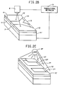
- Figure 1 is a perspective view of a photohardenable film removably adhered to a support.
- Figure 2a is a schematic representation of a preferred way for forming an optical waveguide in a film on a support.
- Figure 2b is a schematic representation of a second preferred way for forming an optical waveguide having a Y configuration in a film on a support.
- Figure 2c is a schematic representation of a third preferred way for forming an optical waveguide having a different configuration in a film on a support.
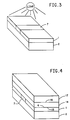
- Figure 3 depicts an optional step of flooding the film having a waveguide on a support with light.
- Figure 4 shows a laminated structure comprising from top to bottom a support, a photohardenable layer, a film having a waveguide, and another support.
- Figure 5 illustrates an optional step of flooding the structure of Figure 4 with light.
- Figure 6 is the structure of Figure 4 or 5 with one of the supports removed.
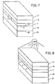
- Figure 7 is a perspective view of an optical waveguide device comprising from top to bottom a support, a photohardenable or photohardened layer, a film having a waveguide, a photohardenable layer, and a support.
- Figure 8 shows the step of hardening the device of Figure 7 by flooding it with light.
- Figure 9 shows the step of hardening the element of Figure 7 or the device of Figure 8 by heating it.
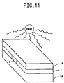
- Figure 10 is a perspective view of an optical waveguide device for use in integrated optical systems, the device comprising from top to bottom a first hardened layer, a hardened film having a waveguide, and a second hardened layer.
- Figure 11 shows the step of stabilizing the device of Figure 10 by heating it.
- Figure 12a illustrates an optical fiber composite structure
- Figure 12b illustrates an optical waveguide device.
- Figure 13a illustrates an optical fiber composite structure having a center axis.
- Figure 13b illustrates the middle portion of an optical waveguide device.
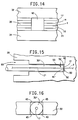
- Figure 14 shows a cross section of a waveguide device illustrating the different layers surrounding a symmetrical opening.
- Figure 15 shows a cross section of an optical fiber inserted in the symmetrical opening of an optical waveguide device.
- Figure 16 illustrates a cross section perpendicular to the one shown in Figure 15.
- Figure 17 illustrates a method of inserting liquid adhesive in the symmetrical opening of a waveguide device.
- Figure 18 illustrates the middle portion of an optical waveguide device with a symmetrical opening having two pockets.
- This invention pertains to a method of coupling an optical fiber with an optical waveguide device through a symmetrically disposed opening located in front of the waveguide. This greatly facilitates the alignment of the waveguide embedded in the device with the waveguide of the optical fiber, and alleviates the need for accurate and very expensive equipment, which is otherwise required for the waveguide alignment.
- an element comprising a substantially dry photohardenable film 1 removably adhered to a support 2.
- the film 1 has a first surface 3 and a second surface 4.
- the support similarly has a first surface 5 and a second surface 6.
- the first surface 5 of the support 2 is removably adhered to the first surface 3 of the film 1.
- the surfaces 3, 4, 5 and 6 of the film 1 and the support 2 are preferably substantially flat.
- the film 1 may have a thickness in the range of 2 micrometers through 15 micrometers or above, preferably in the range of 4.5 micrometers through 8.0 micrometers, and more preferably about 5.3 micrometers.
- the first step of the method of making the preferred devices according to the present invention comprises exposing to light at least a first region 7 of the film 1 polymerizing at least one monomer in the film 1 and changing the refractive index of the region 7 to form at least a first optical waveguide.
- the term waveguide is defined by those skilled in this art to include the entire area that transmits radiant energy. This technically includes some area just around the exposed region can by considered to substantially be the waveguide.
- a polymerization reaction is induced in the exposed region. It is believed that there is interdiffusion between the exposed and unexposed regions, at least near the interface of these regions.
- This interdiffusion changes and typically increases the density of the exposed region raising its refractive index creating a lens-like exposed region directing the light in a self focused fashion to create a narrow smooth walled waveguide of approximately the same dimension as a mask area or light beam width.
- Three ways for performing this first step are illustrated in Figures 2a, 2b and 2c.
- a focused laser light source 8 exposes the region 7 to form the waveguide.
- a translational mechanism 9 is connected to the laser light source 8 and/or the support 2 for moving the laser light source 8, the support 2 or both, to create the waveguide having a desired and/or predetermined pattern.
- the exposed region 7 has a substantially elongated box configuration having an optical axis 10 through the longitudinal center of the region 7.
- a physical cross section of the exposed region 7 perpendicular to the optical or center axis 10 is substantially rectangular.
- On both sides of the region 7 are remaining unexposed regions 11 of the film 1.
- Figure 2b shows an alternate way for exposing a region 7 ⁇ .
- a non-focused laser light source 8' is generally directing actinic radiation toward the element of Figure 1.
- An opaque mask 12 is positioned between the laser light source 8 and the film 1, typically contacting and covering the second film surface 4.
- the mask 12 has at least a patterned area 13 therein through which actinic radiation from the light source 8' exposes region 7'.
- the patterned area can have any desired configuration, including the substantially Y configuration shown in Figure 2b.
- the region can have one end adapted to inlet or outlet light connected to a plurality of ends (e.g., 2, 3, 4...) adapted to inlet or outlet light.
- ends e.g., 2, 3, 4
- FIG. 2c A third way for performing the exposing step of the present method is illustrated in Figure 2c.
- actinic radiation from a light source 8" exposes a first region 7" and a second region 7′′′ of the film 1 through an opaque mask 12'.
- This mask 12' has first and second areas 13' and 13" for the light to pass through exposing regions 7" and 7′′′, respectively.
- the second area 13" approaches and is in part parallel to the first area 13'.
- the exposed second region 7′′′ and the corresponding waveguide can be positioned to exhibit evanescent coupling of light injected into one of the waveguides by gradually leaking or coupling the injected light into the other waveguide.
- Figures 2a, 2b and 2c illustrate the making of optical waveguide elements, useful in making optical waveguide devices, which in turn are useful in integrated optical systems.
- Figure 3 illustrates an optional step which follows the exposing step.
- the element resulting from the exposure step can be flooded with light, such as broadband ultraviolet light. This polymerizes some of at least one monomer in the film and typically most or all of one or all of the monomers in the film. This may allow for easy removal or attachment of the support 2.
- This resulting optical waveguide element can similarly be used in making optical waveguide devices, which devices are preferably used in the present invention.
- a first substantially dry photohardenable layer 14 is laminated to the second film surface 4.
- the first layer 14 has first and second surfaces 15 and 16, respectively.
- the first layer 14 first surface 15 is laminated to the second film surface 4 by placing them in intimate contact and controllably applying pressure with rollers to remove air between the film 1 and layer14.
- the first layer 14 is tacky. If the optional flooding step illustrated in Figure 3 is not performed, then the film 1 is also tacky. Thus, the film 1 and first layer 14 easily adhere to one another.
- a support 17 is removably adhered to the second surface 16 of the first layer 14.
- Figure 4 illustrates another optical waveguide element useful in making optical waveguide devices, which devices are preferably used in the present invention.
- Figure 5 shows an optional flooding step similar to that illustrated in Figure 3, except the element being flooded is modified as described in relation to Figure 4.
- the element resulting from the first lamination step can be flooded with light, such as broadband ultraviolet light. This polymerizes some of at least one monomer (and typically most or all of one or all of the monomers) in the first layer 14 and further polymerizes some of the at least one monomer in the film 1 (if not already polymerized by a previous flooding step). Extensive crosslinking or polymerization occurs between the monomer(s) of the layer 14 adjacent to the monomer(s) of the film 1 forming a diffuse boundary line or region.
- the resulting optical waveguide element is also useful in making an optical waveguide device in accordance with this invention.
- Figure 6 shows the element after the next step of removing the support 2 from the film 1 first surface 3.
- a second substantially dry photohardenable layer 18 is laminated to the film 1 first surface 3.
- the second layer 18 has first and second surfaces 19 and 20, respectively.
- the second layer 18 first surface 19 is laminated to the film first surface 3 by placing it in intimate contact and controllably applying pressure with rollers removing air between the film 1 and second layer 8.
- the second layer surfaces 19 and 20 are tacky and, thus, easily adhere to the film 1.
- a support 21 is removably adhered to the second layer second surface 20.
- Figure 8 illustrates a step of hardening the structure depicted in Figure 7 by flooding it with light, such as broadband ultraviolet light.
- light such as broadband ultraviolet light.
- broadband ultraviolet light means light in the spectral region of about 350 through 400 nanometers. This step occurs for minutes, preferably 5, but can last longer. If this is the first flooding step, then this is the first polymerization of at least one monomer (and typically most or all of one or all monomers) in the remaining regions 11 in the film 1 and the first and second layers 14 and 18, respectively. It further polymerizes the at least one monomer in the region 7 of the film 1. If this is not the first flooding step, it polymerizes at least one monomer in the second layer and continues polymerizing the at least one monomer in the rest of the element.
- Some crosslinking or polymerization occurs between the previously polymerized film 1 and the monomer(s) in the second layer 18 forming a boundary line or region that is more evident than if the film 1 had not previously been flooded with light. Further, if this is not the first flooding step, for instance if buffer layer 14 was previously hardened by flooding it with light as illustrated in Figure 5, then it would be preferred to harden the film 1 and the buffer layer 18 of the element illustrated in Figure 8 by flooding light first through support 21, layer 18, film 1, layer 14, and then support 17. In other words, the structure should be flooded such that light passes through unhardened layers or films before previously hardened ones.
- any one or all of the buffer layers and the film with a waveguide formed therein can be hardened by flooding them with light before the layers or film are laminated to the other parts.
- a device results having at least one buried channel waveguide in a laminated and photohardened matrix useful in integrated optical systems.
- Figure 9 illustrates another possible step of hardening the structure depicted in Figure 7 by heating it.
- the layers and film can be heated before, in combination with, after, or in lieu of the light flooding step to harden or further harden the device.
- This heating step occurs at a temperature in the range of about 50 o C through 200 o C and preferably in the range of about 90 o C through 150 o C for a duration of minutes, preferably 5.
- Photohardenable compositions are typically less sensitive to temperatures up to 100 o C than above 100 o C. However, hardening may be initiated as low as 50 o C of held at the temperature for a sufficient period of time. As the temperature is increased beyond 100°C, thermally initiated hardening increases significantly.
- a maximum refractive index increase in the localized waveguide region as measured by an ASUJENA Interphako microscope occurs in the film in the range of 0.001 through 0.040 measured at 551 nanometers wavelength.
- the waveguide is transparent in the range of 0.6 through 1.6 micrometers wavelength. It is effectively transparent at 1.3 micrometers for single mode operation.
- the maximum refractive index of the matrix except in and near the waveguide is in the range of 1.45 through 1.60, measured at white light from an incadescent source, depending on formulation and/or extent of interlayer diffusion from adjoining layers or film of different indexes.
- the refractive index is determined by using an ABBE refractometer manufactured by Karl Zeiss.
- the supports 17 and 21 can be removed from the device resulting from the hardening step as shown in Figure 10.
- Figure 11 shows an optional, but preferred, step of stabilizing the device shown in Figure 10 by heating it, typically after the hardening step.
- This heating step similarly occurs at a temperature in the range of about 50 o C thorough 200 o C and preferably in the range of about 90 o C through 150 o C.
- this stabilizing step occurs longer than the hardening step.
- the stabilizing step occurs in the range of about 20 minutes through 2 hours and more preferably for about an hour.
- This heating makes the device more environmentally stable. Further, this heating provides thermal stabilization of optical and mechanical properties allowing operation of the resulting device over a wide range of temperatures without modification of the device properties.
- the first and second layers 14 and 18, respectively have equal thicknesses since the films 14 and 18 are substantially identical, thus inherently serving the "symmetry" requirement. It is preferable for the purposes of this invention to select and cut the pieces of films 14 and 18 from adjacent areas of the same roll of film, in order to ensure identical thickness.
- One of the advantages of this arrangement is the ease of adding one or more substantially dry photohardenable or photohardened layers on each side with or without a waveguide or grating, and build up any desired thickness, still serving the "symmetry" requirement.
- the hardened device matrix is substantially homogenous in composition and refractive index except in and near the waveguide.
- the waveguide has a refractive index about 0.005 and 0.060 greater than the surround.
- the composition and refractive index in each exposed region is substantially homogenous in composition and refractive index.
- Figures 12a and 13a illustrate a conventional optical fiber composite structure 39 comprising a glass part 30' and an outside protective envelope 36, having usually a diameter of approximately 250 micrometers.
- the outside protective envelope 36 is immaterial, while the glass part 30' is of substantial importance.
- the glass part 30' may be referred to also as the optical fiber, the fiber, the glass fiber, or the optical glass fiber, without implying distinction between these terms, which should be considered as synonyms.
- glass is the predominant material of construction of optical fibers at the present time, other materials of construction having similar physical characteristics, such as for example polymethylmethacrylate, may also be utilized in the practice of this invention.
- the optical fiber has a central region 7' of different (usually higher) refractive index than the rest of the fiber, which serves as a waveguide.
- the diameter of the optical fiber is nominally 125 micrometers, while that of the waveguide is about 8-9 micrometers.
- some light travels outside the waveguide.
- the optical fiber 30', the depressed cladding area (not shown) if present, as well as the waveguide are characterized by a common optical or center axis A'-A', which is also an axis of symmetry.
- the optical fiber 30' has a first end surface 41', which is substantially perpendicular to the center axis A'-A'. The intersection of the waveguide 7' and the first end surface 41' define a first end-point 40'.
- Figure 12b illustrates an optical waveguide device 38, which comprises a waveguide 7.
- the waveguide 7 has a second optical or center axis A-A, illustrated in Figure 13b, and a second end-point 40.
- an opening 42 of substantially square cross-section disposed symmetrically in front of the second end-point 40 in a direction substantially parallel to the direction of the waveguide 7.
- the opening has a second end-surface 41.
- the second end-point 40 may also be defined as the cross-section of the waveguide 7 and the end-surface 41.
- axis A-A is perpendicular to the square cross section of the opening 42, and it passes through the intersection of the diagonals of the square cross section at any point along the opening 42.
- insertion cavity 60 Opposite to the second end-point 40, there is preferably an insertion cavity 60, which in combination with the opening 42 gives the appearance of a "T" shape.
- the middle portion 30 of the optical waveguide device 38 is formed as described in other sections of this discussion, wherein the waveguide is photoimaged in a "Waveguide Layer", followed by sandwiching the "Waveguide Layer” 1 between a pair of "Inner Buffer layers” 14 and 18, as well as a pair of "Outer Buffer layers” 17 and 21.
- the layers of each pair are preferably selected from adjacent areas of the same photopolymer sheet, so that the thickness is the same for all practical purposes. This procedure ensures that the waveguide 7, and therefore the second end point 40, are equidistant from the outer surfaces 47 and 49 of the middle portion 30. These surfaces are also substantially parallel to each other.
- Forming the opening 42 is preferably performed by ablation and in the form of a slot as better shown in Figure 13b. It is preferable that the opening 42 is ablated by the use of a laser, and more preferably by an excimer laser.
- a method for providing excimer ablated fiber channels or openings for passive (without need of alignment equipment) coupling involves a computer controlled image processing and positioning system. The excimer laser is masked by a rectangular aperture and is projected onto the optical waveguide device though a 15x reduction lens. The aperture's width is adjusted until the correct channel width for passive coupling is achieved. For preferred present applications, this width is approximately 115 to 125 micrometers wide (as measured by the computer) at the plane of the middle portion 30.
- This width is substantially the same as the thickness of the middle portion 30, so that a substantially square cross-section of the opening is achieved.
- a "sample” channel is preferably created away from the work area. This sample channel is digitized and analyzed for width; the center and angular orientation are determined by an image processing system, and this image along with the rest of the data, are stored as a reference that will be used to align other waveguides. At this point a waveguide is brought into the field of view, and the optical waveguide device is aligned laterally and rotationally, iteratively, until preferably within tolerance of the reference channel alignment ⁇ 0.5 micrometers laterally, ⁇ 0.25 degrees rotationally).
- the insertion cavity 60 may be also formed using similar techniques.
- packaging layers 32 and 34 are laminated on the parallel surfaces 47 and 49 of the middle portion 30. After lamination, the front part of this laminate may be microtomed to form a flat front side 51.
- FIG 14 A more detailed view of a cross-section of the opening 42 and the surrounding composite laminate of different layers of the device 38 is depicted in figure 14, wherein the "Waveguide layer” 1 is sandwiched between a pair of “Inner Buffer layers” 14 and 18, a pair of “Outer Buffer Layers” 17 and 21, and a pair of packaging layers 32 and 34.
- the top and bottom of the opening 42 are part of the packaging layers 32 and 34, while the sides are part of the rest of the layers.
- the optical fiber 30' is inserted initially through the insertion cavity 60 and then through the opening 42, until the first end surface 41' assumes a predetermined distance 50 from the second end surface 41, as better shown in Figure 15.
- This distance should preferably be between 2 and 10 micrometers and more preferably between 4 and 6 micrometers.
- bevelling 52 is performed at the end portion of the fiber.
- the bevelled part 52 should not reach the depressed cladding area (not shown), which surrounds the first waveguide 7', if present. More preferably, the bevelled part should have a depth 53 between 2 and 10 micrometers, and even more preferably between 4 and 6 micrometers.
- the diameter of the optical fiber 30' is substantially equal to the side of the cross section of the opening 42.
- the alignment and self-centering may be assured to have much better reproducibility and accuracy when the diameter of the optical fiber 30' is somewhat larger than the side of the square cross section of the opening 42.
- the diameter of the optical fiber should preferably be 2 to 10 micrometers larger, and more preferably 4 to 6 micrometers larger.
- a liquid is placed between the ends of the waveguides to fill such gaps.
- This liquid should have a refractive index which matches as close as possible the refractive indices of the waveguides involved. It is preferable that this liquid possesses adhesive characteristics in order to secure the optical fiber and the respective device in place. It is even more preferable that the curing of the adhesive liquid is a photohardenable one, and thus is cured by a photohardening mechanism. This is preferred not only because most of the steps of making the devices of the instant invention involve actinic radiation, but also and more importantly because an independent heating step may be employed for expanding the liquid before its cure.
- thermally cross lincable polymers may also be used as long as they substantially cross link at such temperatures which do not interfere with the thermal steps necessary in the practice of this invention.
- the technique of using such adhesive formulations may be applied not only for the devices of the present invention, but also in any other case, where the free ends of two embedded waveguides come high proximity or contact for the purposes of coupling, including connectors, couplers, splitters, fiber embedded waveguides, and the like, as well as combinations thereof.
- a photohardenable adhesive is used to secure the fiber in place and eliminate air-gap regions between the waveguides. It should be realized that even after insertion of the optical fiber in the opening 42, a remanent opening 43, as better shown in Figure 16, resulting from the square cross section of the opening 42 and the circular cross section of the optical fiber 30' is left behind. Thus, the remanent opening 43 may accept the adhesive by capillary action, even after the insertion has taken place. It is, however, preferable that the adhesive is applied before the insertion step of the optical fiber 30'.
- the application of the adhesive may be conducted by means of a microtube, such as the one used in example 2, and as illustrated in Figure 17.
- a thin wire with a loop may be used.
- An example of such a wire is one made of gold for inertness, and having a diameter of 10 to 30 micrometers.
- a drop may be placed in the close vicinity of the insertion cavity 60, so that the drop overlaps the lip 69 of the cavity. Due to wetting and surface tension phenomena, the adhesive 68 fills the opening 42 first and then the insertion cavity 60. For better wetting, the adhesive should have lower surface tension than the surface tension of the optical fiber 30' and the surface tension of the opening 42 and cavity 60.
- the adhesive 68 Since, upon subsequent insertion of the optical fiber 30', some of the adhesive 68 also overflows into the front flat side 51 within a small area surrounding the optical fiber 30', it is preferable that this flat side has also higher surface tension than the adhesive.
- Monomers, oligomers, polymers, initiators, chain transfer agents and other constituents like the ones used for the fabrication of the devices, and described herein may also be used for making the optically matching liquid, which as aforementioned, is preferably also an adhesive when photohardened. Of course, any other materials may be used as long as the requirements set forth are met.
- one or more pairs of pockets 62 and 64, as illustrated in Figure 18 may be also ablated along the opening 42. These pockets, after receiving the liquid adhesive, act as anchoring sites to secure better the optical fiber 30' in the opening 42.
- the pockets are preferably 10 to 50 micrometers, and more preferably 10 to 20 micrometers out from the edge of the opening 42. They are preferably located approximately 100 to 200 micrometers from the end surface 41.
- the pockets 62 and 64 create a region where liquid adhesive can further bond to the optical waveguide structure and the glass fiber, providing a plug which prevents the optical fiber from being pulled out easily and helps pin the optical fiber to the waveguide interface, preventing displacement under temperature-induced shear forces.
- the step of inserting the optical fiber 30' into the opening 42 is conducted at temperatures, which are somewhat elevated as compared to room temperature, in order to facilitate the insertion and avoid delamination of the different layers of the waveguide device 38.
- the waveguide device 38 is plastisized or softened just adequately to facilitate insertion of part 30, and prevent delamination without causing unacceptable distortion of the waveguide device and without affecting the self centering of the waveguides 7 and 7' with respect to each other during the insertion step.
- Temperatures of the order of 40 - 50 °C are preferable for this step.
- the use of heat provides a light softening of the material during fiber insertion and it is an important part helping prevent unduly high forces from delaminating the material
- immediate insertion is also important to prevent delamination because of possible swelling as liquid adhesive diffuses into the surround.
- the timing of insertion versus swelling can provide additional tolerance for the width of the ablated opening 42, in cases where the ablated size deviation results in a width slightly larger than that of a typical optical fiber, or greater than 124 micrometers, when a somewhat delayed insertion would be preferable.
- the important consideration is often to avoid undue pressure from the optical fiber 30' as it is inserted in to an opening of inadvertently ablated incorrect low dimensions. In general, however, immediate insertion of the optical fiber is preferred.
- Unpolymerized liquid adhesives may have a tendency to free debris from the edges of the opening, the longer the adhesive stays unpolymerized as a liquid in the opening 42. This effect can produce a collection of floating debris within the opening itself.
- the preferred fiber coupling technique is to push the fiber in soon after insertion of liquid adhesive and rapidly position it directly in front of the waveguide so that debris cannot be compacted at the end of the slot.
- An alternative approach is to flush out any debris with fresh liquid adhesive.
- the liquid adhesive also diffuses into a diffusion region (nominally 40 micrometers) providing a distribution of shear forces during heat cycling between the glass, whose expansion coefficients are nominally one part per million, and the optical waveguide device, including the adhesive, whose expansion coefficient is nominally 100 to 120 parts per million. This distribution of shear forces helps prevent the breakdown of the bond of the glass fiver 30' to the device 38 during temperature cycling.
- the temperature is raised further to a higher predetermined point, and the photohardening or photocuring of the adhesive is conducted at this higher point or level of temperature.
- the higher level of temperature has to be adequately high in order to reduce or prevent temperature versus optical-throughput oscillations of the coupled device at temperatures lower than the predetermined point. These oscillations manifest themselves as repeated cycles of increase followed by decrease of the optical throughput of the coupled device as the temperature of the device, at which each measurement is made, changes. Temperatures of the order of 60 to 90 °C are preferable with the presently employed photopolymers.
- the waveguide device 38 when the photocuring is conducted at an elevated temperature, the waveguide device 38, made of layers of photopolymers, is in a highly expanded state as compared to the optical fiber 30', and the opening 42 takes a larger amount of liquid photohardenable adhesive.
- the coupled device made in this manner, is brought to lower temperatures, as the temperature continues decreasing, high compression is developed by the large shrinkage of the waveguide device. This compression is applied on the glass part 30' of the optical fiber 39 through the mass of the excessive adhesive, thus resisting the formation of the gap.
- adhesion promoters are very important, so that the coupling may perform under adverse conditions.
- the preferred adhesion promoters are silane based promoters since they mainly promote adhesion to glass, which is usually the weak point of adhesion in this application, if and when adhesive failure occurs.
- Methacryloxypropyltrimethoxy silane is preferred.
- examples of other photopolymerizable silane adhesion promoters, which may be used in the practice of this invention include but are not limited to:
- the concentration of the silane promoter in the adhesive formulation could be as broad as 0.5% to 97% by weight. A more preferred range is 1 to 25% and an even more preferred range is 8-16% by weight.
- the photohardenable base and buffer layers used herein are thermoplastic compositions which upon exposure to actinic radiation form crosslinks or polymers of high molecular weight to change the refractive index and rheological character of the composition(s).
- Preferred photohardenable materials are photopolymerizable compositions, such as disclosed in United States Patent 3,658,526 (Haugh) and more preferred materials are described in U. S. Patents 4,942,102, 4,942,112, and in copending application Serial Number 07/288,916* filed December 23, 1988 and assigned to E. I. du Pont de Nemours and Company, Incorporated.
- a binder is the most significant component of a substantially dry photopolymerizable base or layer in terms of what physical properties the base or layer will have while being used in the invention.
- the binder serves as a containing medium for the monomer and photoinitiator prior to exposure, provides the base line refractive index, and after exposure contributes to the physical and refractive index characteristics needed for the base layer of buffer layer.
- Cohesion, adhesion, flexibility, diffusibility, tensile strength, in addition to index of refraction are some of the many properties which determine if the binder is suitable for use in the base layer or the buffer layer.
- * US-A-4,994,347 (issued on February 19, 1991).
- Dry base or layer photohardenable elements contemplate to be equivalent are photodimerizable or photocrosslinkable compositions such as disclosed in United States Patent 3,526,504 (Celeste) or those compositions in which hardening is achieved by a mechanism other than the free radical initiated type identified above.
- the photopolymerizable base or layer is a solid sheet of uniform thickness it is composed of three major components, a solid solvent soluble performed polymeric material, at least one liquid ethylenically unsaturated monomer capable of addition polymerization to produce a polymeric material with a refractive index substantially different from that of the performed polymeric material, or binder, and a photoinitiator system activatable by actinic radiation.
- the base or layer is a solid composition, components interdiffuse before, during and after imaging exposure until they are fixed or destroyed by a final uniform treatment usually by a further uniform exposure to actinic radiation. Interdiffusion may be further promoted by incorporation into the composition of an otherwise inactive plasticizer.
- the composition may contain solid monomer components capable of interdiffusing in the solid composition and reacting with the liquid monomer to form a copolymer with a refractive index shifted from that of the binder.
- the preformed polymeric material and the liquid monomer are selected so that either the preformed polymeric material or the monomer contains one or more moieties taken from the group consisting essentially of substituted or unsubstituted phenyl, phenoxy, naphthyl, naphthyloxy, heteroaromatic groups containing one to three aromatic rings, chlorine, and bromine and wherein the remaining component is substantially free of the specified moieties.
- the photopolymerizable system hereinafter is identified as a "Monomer Oriented System” and when the polymeric material contains these moieties, the photopolymerizable system hereinafter is identified as a "Binder Oriented System.”
- the stable, solid, photopolymerizable compositions preferred for this invention will be more fully described by reference to the "Monomer Oriented System” and "Binder Oriented System.”
- the Monomer Oriented System is preferred for the base layer.
- the monomer of the Monomer Oriented System is a liquid, ethylenically unsaturated compound capable of addition polymerization and having a boiling point above 100 C.
- the monomer contains either a phenyl, phenoxy, naphthyl, naphthoxy, heteroaromatic group containing one to three aromatic rings, chlorine or bromine.
- the monomer contains at least one such moiety and may contain two or more of the same or different moieties of the group, provided the monomer remains liquid.
- Contemplated as equivalent to the groups are substituted groups where the substitution may be lower alkyl, alkoxy, hydroxy, carboxy, carbonyl, amino, amido, imido or combinations thereof provided the monomer remains liquid and diffusible in the photopolymerizable layer.
- Preferred liquid monomers for use in the Monomer Oriented System of this invention are 2-phenoxyethyl acrylate, 2-phenoxyethyl methacrylate, phenol ethoxylate acrylate, 1-(p- chlorophenoxy) ethyl, p-chlorophenyl acrylate, phenyl acrylate, 1-phenylethyl acrylate, di(2-acryloxyethyl) ether of bisphenol-A, and 2-(2-naphthyloxy) ethyl acrylate.
- monomers useful in this invention are liquids, they may be used in admixture with a second solid monomer of the same type, e.g., N-vinyl-carbazole, ethylenically unsaturated carbazole monomers such as disclosed in Journal of Polymer Science: Polymer Chemistry Edition , Vol. 18, pp. 9-18 (1979) by H. Kamagawa et al., 2-naphthyl acrylate, penta-chlorophenyl acrylate, 2,4,6-tribromophenyl acrylate, and bisphenol A diacrylate, 2-(2-naphthyloxy) ethyl acrylate, and N-phenyl maleimide.
- a second solid monomer of the same type e.g., N-vinyl-carbazole, ethylenically unsaturated carbazole monomers such as disclosed in Journal of Polymer Science: Polymer Chemistry Edition , Vol. 18, pp. 9-18 (1979) by
- the solvent soluble polymeric material or binder of the Monomer Oriented System is substantially free of phenyl, phenoxy, naphthyl, naphthyloxy, heteroaromatic group containing one to three aromatic rings, chlorine and bromine.
- Preferred binders for use in the Monomer Oriented system of this invention are cellulose acetate butyrate polymers; acrylic polymers and inter polymers including polymethyl methacrylate, methyl methacrylate/methacrylic acid and methylmethacrylate/acrylate acid copolymers, terpolymers of methylmethacrylate/C2-C4 alkyl acrylate or methacrylate/acrylic or methacrylic acid; polyvinylacetate;polyvinylacetate; polyvinyl acetal, polyvinyl butyral, polyvinyl formal; and as well as mixtures thereof.
- the monomers of the Binder Oriented System is a liquid ethylenically unsaturated compound capable of addition polymerization and having a boiling point above 100 C.
- the monomer is substantially free of moieties taken from the group consisting essentially of phenyl, phenoxy, naphthyl, naphthyloxy, heteroaromatic group containing one to three aromatic rings, chlorine and bromine.
- Preferred liquid monomers for use in Binder Oriented Systems of this invention include decanediol diacrylate, iso-bornyl acrylate, triethylene glycol diacrylate, diethyleneglycol diacrylate, triethylene glycol dimethacrylate, ethoxyethoxyethyl acrylate, triacrylate ester of ethoxylated trimethylolpropane, and 1-vinyl-2-pyrrolidinone.
- Binder Oriented Systems While monomers used in Binder Oriented Systems are liquids, they may be used in admixture with a second solid monomer of the same type, e.g., N-vinylcaprolactam.
- the solvent soluble polymeric material or binder of the Binder Oriented system contains in its polymeric structure moieties taken from the group consisting essentially of phenyl, phenoxy, naphthyl naphthyloxy or heteroaromatic group containing one to three aromatic rings as well as chloro or bromo atoms. Contemplated as equivalent to the groups are substituted groups where the substitution may be lower alkyl, alkoxy, hydroxy, carboxy, carbonyl, amido, imido or combinations thereof provided the binder remains solvent soluble and thermoplastic.
- the moieties may form part of the monomeric units which constitute the polymeric binder or may be grated onto a pre-prepared polymer or interpolymer.
- the binder of this type may be a homopolymer or it may be an interpolymer of two or more separate monomeric units wherein at least one of the monomeric units contains one of the moieties identified above.
- Preferred binders for use in the Binder Oriented System include polystyrene, poly (styrene/acrylonitrile), poly(styrene/ methyl methacrylate), and polyvinyl benzal as well as admixtures thereof.
- the same photoinitiator system activatable by actinic radiation may be used in either the Monomer Oriented System or the Binder Oriented System.
- the photoinitiator system will contain a photoinitiator and may contain a sensitizer which extends the spectral response into the near U.V. region and the visible spectral regions.
- Preferred photoinitiators include CDM-HABI, i.e., 2-(o-chlorophenyl)-4,5-bis( m -methoxyphenyl)-imidazole dimer; o -CI-HABI, i.e., 1,1'-Biimidazole, 2,2'-bis-( o -chlorophenyl)-4,4', 5,5'- tetraphenyl-; and TCTM-HABI, i.e., 1H-Imidazole, 2,5-bis( o -chlorophenyl)-4-3,4-dimethoxyphenyl-, dimer eac of which is typically used with a hydrogen donor, e.g., 2-mercapto-benzoxazole.
- a hydrogen donor e.g., 2-mercapto-benzoxazole.
- Preferred sensitizers include the following: DBC, i.e., Cyclopentanone, 2,5-bis-(diethylamino)-2-methylphenyl)methylene) DEAW, i.e., Cyclopentanone, 2,5-bis-((4-(diethylamino)phenyl)methylene); and Dimethoxy-JDI, i.e., 1H-Inden-1-one, 2,3-dihydro-5,6-dimethoxy-2-((2,3,6,7-tetrahydro-1H,5H-benzo[i,j]quinolizine-9-yl)-methylene).
- DBC i.e., Cyclopentanone, 2,5-bis-(diethylamino)-2-methylphenyl)methylene
- DEAW i.e., Cyclopentanone, 2,5-bis-((4-(diethylamino)phenyl)methylene
- the solid photopolymerizable compositions of this invention may contain a plasticizer.
- Plasticizers of this invention may be used in amounts varying from about 2% to about 20% by weight of the compositions preferably 5 to 15 wt. %.
- Preferred plasticizers for use in simple cellulose acetate butyrate systems are triethyleneglycol dicaprylate, tetraethyleneglycol diheptanoate, diethyl adipate, Brij 30 and tris-(2-ethylhexyl)phosphate.
- triethyleneglyco dicaprylate, diethyl adipate, Brij 30, and tris(2-ethylhexyl)- phosphate are preferred in "Monomer Oriented Systems" where Cellulose acetate butyrate is the binder.
- Such components include: ultraviolet radiation absorbing material, thermal stabilizers, hydrogen donors, oxygen scavengers and release agents.
- Amounts of ingredients in the photopolymerizable compositions will generally be within the following percentage ranges based on total weight of the photopolymerizable layer: monomer, 5-50%, preferably 15-35% initiator 0.1-10%, preferably 1-5%; binder, 25-75%, preferably 45-65%; plasticizer, 0-25%, preferably 5-15%; other ingredients 0-5%, preferably 1-4%.
- the supports can be any substance transparent to actinic radiation that provides sufficient support to handle the combined base. and layer. Preferably the support is transparent to light in the spectral region of 0.6 through 1.6 micrometers wavelengths.
- the term "support” is meant to include natural or synthetic supports, preferably one which is capable of existing in a flexible or rigid film or sheet form.
- the support or substrate could be a sheet or film of synthetic organic resin, or a composite of two or more materials.
- Specific substrates include polyethylene terephthalate film, e.g., resin-subbed polyethylene terephthalate film, flame or electrostatic discharge treated polyethylene terephthalate film, glass, cellulose acetate film, and the like.
- the thickness of the supports has no particular importance so long as it adequately supports the film or layer removably adhered to it. A support thickness of about twenty-five(25) to fifty (50) micrometers using polyethylene terephthalate provides sufficient rigidity.
- a substantially dry photohardenable (active) film (base or waveguide layer) of about 5.3 micrometers thick, having the ingredients listed in Table I, coated on a 25 micrometer thick clear polyethylene terephthalate support, in approximately a 3 inch X 4 inch section, is exposed to broad band ultraviolet light in the spectral range of 350 to 400 nanometers through a conventional chrome-plated glass photo-mask to produce a 1 X 4 (one waveguide end to four waveguide ends or four to one) coupler waveguide pattern. After exposure and then an appropriate delay time of about 15 minutes, the mask is removed.
- a first substantially dry photohardenable layer (inner buffer layer) of about 30 micreometers thick, having the ingredients listed in Table II, coated on a 25 micrometers thick clear polyethylene terephthalate support, is laminated to the film surface over the waveguide.
- a second photohardenable layer (inner buffer layer) of identical composition and structure, as the first buffer layer, with support, is laminated to the opposite surface of the film (base or waveguide layer) and flooded as above.
- the laminate is subsequently flooded with broadband ultraviolet light in the spectral range on 350 to 400 nanometers.
- a third and fourth buffer layer (outer buffer layers) of a composition as shown in Table III, and a structure as the other buffer layers are laminated to the first and second buffer layers, respectively, with flooding between each lamination and subsequent removal of the buffer layer support to form an optical waveguide device having a buried channel waveguide.
- the resultant device is heated at 90 o C for 60 minutes to achieve thermal stability.
- the particular formulations described in Tables IV, V, and VI were used to create a single-mode guide operating at 1290 nanometer wavelength, as described in Example 1.
- the waveguide nominal dimension was 7.5 ⁇ 0.2 micrometers including both the mask dimension and the waveguide layer thickness.
- the inner and the outer buffer layers were approximately 28 micrometers each.
- the total thickness of the sample was approximately 123 ⁇ 1 micrometers, with an embedded straight single-mode waveguide having dimensions 7.5 micrometers ⁇ 0.2 micrometer in both waveguide layer thickness and waveguide width.
- the guide operated single mode at 1300 nanometers with a typical loss of 0.4 to 0.5 dB/cm.
- the sample was then ablated by an excimer laser for creation of an opening in the form of a slot 42, as illustrated in Figure 13b.
- the ablated opening was approximately 121 ⁇ 1 micrometers in width and 470 micrometers in length, with an insertion region having a depth of approximately 50 micrometers. This insertion region protects the opening from damage during microtoming, which is usually performed at a later stage.
- the excimer laser wavelength was 248 nanometers. Using approximately 360 millijoules per pulse and a 10-hertz repetition rate, it took 30 seconds to create the individual slot.
- One optical fiber (AT&T 8.9-micrometer mode field and 8.3-micrometer core lightguide) having a nominal diameter of 125 ⁇ 1 micrometers was initially beveled in the front, and then coupled at each end of the waveguide.
- the beveled fiber had a taper disposed at approximately 30 degrees angle from the center axis of the fiber.
- the acrylate coating surrounding the fiber was stripped approximately 550 to 580 micrometers from the end of the cleaved optical fiber glass.
- the coupling of the fiber to the device was conducted as follows:
- the angles between the center axes of the waveguide of the devise and the corresponding center axes of the fibers at each end of the waveguide were approximately 0.5 degrees.
- the double coupling (fiber to waveguide to fiber) provided reproducible, stable output when cycled over-45 to +85 o C, at least five times.
- it displayed a throughput Fabry-Perot like optical oscillation, hypothesized to be due to opening up of the fiber-to-waveguide contact, and formation of a gap, as the temperature changes, since the device has an expansion coefficient approximately 100 times higher relative to that of the glass fiber.
- the thickness of the gap changes then with temperature, and affects the throughput according to the relation of the thickness of the gap with respect to the wavelength of the light trying to pass through.
- These repeatable temperature versus optical-throughput oscillations (as the temperature was changed, the optical throughput was decreasing and increasing repeatedly in an oscillation-like fashion) were about ⁇ 5% of the throughput.
- Back reflections into the optical system reinforce the hypothesis of a gap formation between the fiber and the waveguide of the device. The attempt, however, to explain the phenomenon of these oscillations by the hypothesis of the formation of a gap must not be construed as restrictive to the scope of the present invention.
- the final refractive index for the adhesive photopolymer was approximately 1.52.
- Back reflections were approximately two and a half orders of magnitude down from the light input level during temperature monitoring, hypothesized as aforementioned to be due to formation of a small gap between fiber and waveguide.
- a single optical fiber waveguide coupling was created with a substantially identical process and materials except for two "pockets", as indicated in Figure 18, and an additional step of raising the temperature before and maintaining during photocuring at approximately 75 o C.
- the photocuring at higher temperature substantially eliminated Fabry-Perot oscillations.
- the compression may be attributed to the differences of the thermal expansion coefficients of the photopolymers versus that of the glass fiber.
Landscapes
- Physics & Mathematics (AREA)
- General Physics & Mathematics (AREA)
- Optics & Photonics (AREA)
- Engineering & Computer Science (AREA)
- Microelectronics & Electronic Packaging (AREA)
- Optical Couplings Of Light Guides (AREA)
- Mechanical Coupling Of Light Guides (AREA)
- Optical Integrated Circuits (AREA)
Claims (15)
- Un procédé pour coupler une fibre optique (39') à un dispositif optique (38) qui contient un guide d'onde optique (7), ladite fibre optique (39) présentant un coeur de guidage d'onde (7') avec un premier point d'extrémité (40) sur un premier axe central (A'-A') du coeur et ledit guide d'onde (7) présentant un deuxième point d'extrémité (40) sur un deuxième axe central (A-A) du guide d'onde (7), comprenant les étapes consistant :- à former une fente (42) à section transversale sensiblement carrée dans le dispositif optique (38), ladite fente (42) étant disposée de façon symétrique devant le deuxième point d'extrémité (40) et s'étendant à partir de ce deuxième point d'extrémité (40) du guide d'onde (7), la fente (42) étant dimensionnée pour recevoir la fibre optique (39);- à introduire un photopolymère liquide adhésif dans la fente (42);- à insérer la fibre (30') dans la fente (42) de sorte que le premier et le deuxième points d'extrémité (40', 40) soient séparés d'une distance prédéterminée et que le premier axe central (A'-A') soit sensiblement coaxial au deuxième axe central (A-A);caractérisé par les étapes consistant :- à augmenter la température jusqu'à un point prédéterminé; et ensuite- à photodurcir le photopolymère liquide adhésif à la température augmentée en illuminant le photopolymère liquide adhésif avec de la lumière, la température augmentée étant suffisamment élevée pour réduire ou éliminer les oscillations entre la température et la sortie optique au sein du dispositif et qui se produisent pour des températures inférieures à ce point prédéterminé.
- Un procédé selon la revendication 1, dans lequel le photopolymère comprend un stimulateur d'adhérence.
- Un procédé selon la revendication 2, dans lequel le stimulateur d'adhérence est un silane.
- Un procédé selon la revendication 1, comprenant en outre l'étape consistant à former une poche ouverte (62, 64) sur une face de la fente.
- Un procédé selon la revendication 4, dans lequel l'étape consistant à introduire le photopolymère liquide dans la fente (42) est réalisée à travers la poche (62, 64).
- Un procédé selon la revendication 4, dans lequel l'étape consistant à introduire le photopolymère liquide dans la fente (42) est réalisée avant l'étape consistant à insérer la fibre (39) dans la fente (42).
- Un procédé selon la revendication 4, dans lequel l'étape consistant à introduire le photopolymère liquide dans la fente (42) est réalisée après l'étape consistant à insérer la fibre (39) dans la fente (42).
- Un procédé selon la revendication 4, comprenant en outre l'étape consistant à chanfreiner (52) l'extrémité de la fibre optique (39) avant l'étape consistant à l'insérer dans la fente (42).
- Un procédé selon la revendication 4, dans lequel le diamètre de la fibre optique (39) est sensiblement égal à un côté de la section transversale carrée.
- Un procédé selon la revendication 4, dans lequel le dispositif de guide d'onde optique (38) comprend un stratifié composé de couches centrales en photopolymère (1, 14, 17, 18, 21) contenant le guide d'onde (7), et de couches extérieures de conditionnement en photopolymère (32, 34).
- Un procédé selon la revendication 10, dans lequel le diamètre de la fibre optique (39) est légèrement supérieur au côté de l'ouverture carrée du dispositif optique de sorte qu'au moment du couplage de la fibre (39) et du dispositif à guide d'onde optique (38), on obtient un auto-centrage du premier guide d'onde (7') par rapport au deuxième guide d'onde (7).
- Un procédé selon la revendication 11, dans lequel on réalise l'augmentation de la température entre deux niveaux : un niveau inférieur approprié pour empêcher la déstratification des couches pendant l'insertion de la fibre (39) dans la fente (42), et un niveau supérieur approprié pour diminuer les oscillations entre la température et la sortie optique.
- Un procédé selon la revendication 1, consistant en outre pendant l'étape à insérer, à augmenter la température du dispositif de guide d'onde optique (38) à un niveau inférieur au point prédéterminé pour ramollir le dispositif optique (38).
- Un appareil à guide d'onde optique destiné à être utilisé dans le procédé des revendications 1 à 13, comprenant :- un dispositif de guide d'onde optique (38) pour recevoir une fibre optique (39) présentant un coeur de guidage d'onde (7') avec un point d'extrémité (40'), le dispositif (38) comprenant :* une pellicule photodurcie (1) présentant une première surface (4) ainsi qu'une deuxième surface (3) opposée à la première, la pellicule (1) présentant une zone à guide d'onde optique (7) ainsi que d'autres régions (11), le guide d'onde optique (7) présentant un axe central (10 ou A-A) traversant le point d'extrémité (40);* une première couche photodurcie (14) présentant une première surface extérieure (15) et une deuxième surface extérieure (16), la première surface extérieure (15) de la première couche photodurcie étant stratifiée sur la preextérieure (15) de la première couche photodurcie étant stratifiée sur la première surface (4) de la pellicule couvrant une première face du guide d'onde (7), la première couche photodurcie (14) comprenant une ou plusieurs couches;* une deuxième couche photodurcie (18) présentant une première surface extérieure (19) et une deuxième surface extérieure (20), la première surface extérieure (19) de la deuxième couche photodurcie étant stratifiée sur la deuxième face de la pellicule (3) recouvrant une deuxième face du guide d'onde (7), la deuxième couche photodurcie (18) comprenant une ou plusieurs couches.- une première couche de conditionnement (32) présentant une première et une deuxième surface, la première surface de la première couche de conditionnement étant située sur la deuxième surface extérieure (16) de la première couche photodurcie;- une deuxième couche de conditionnement (34) présentant une première et une deuxième surface, la première surface de la deuxième couche de conditionnement étant située sur la deuxième surface extérieure (20) de la deuxième couche photodurcie; et- la pellicule photodurcie (1), la première couche photodurcie (14), la deuxième couche photodurcie (18), la première couche de conditionnement (32) et la deuxième couche de conditionnement (34) définissant une fente (42) à section transversale sensiblement carrée, la fente (42) étant disposée de façon symétrique adjacente au point d'extrémité (40) du guide d'onde optique et partant de ce dernier;- la fente (42) étant apte à recevoir un coeur de guidage d'onde (7') de fibre optique avec le point d'extrémité (40') de la fibre optique adjacent au point d'extrémité de guide d'onde (40);caractérisé en ce que :- la fente (42) présente une ou plusieurs poches (62, 64) pénétrant dans le dispositif (38) selon une direction sensiblement perpendiculaire à l'axe central de guide d'onde optique (10 ou A-A).
- L'appareil à guide d'onde optique selon la revendication 14, comprenant en outre :- une fibre optique (39) présentant un coeur de guidage d'onde (7') avec un point d'extrémité (40'), le coeur de guidage d'onde à fibre optique (7') étant situé à l'intérieur de la fente (42) avec le point d'extrémité de la fibre optique (40') adjacent au point d'extrémité de guide d'onde (40); et- un photopolymère adhésif photodurci (68) à l'intérieur de la fente (42) et la poche (62, 64) disposée entre la fibre optique (39) et le dispositif (38).
Applications Claiming Priority (2)
| Application Number | Priority Date | Filing Date | Title |
|---|---|---|---|
| US59583890A | 1990-10-11 | 1990-10-11 | |
| US595838 | 1990-10-11 |
Publications (3)
| Publication Number | Publication Date |
|---|---|
| EP0480477A2 EP0480477A2 (fr) | 1992-04-15 |
| EP0480477A3 EP0480477A3 (en) | 1992-05-27 |
| EP0480477B1 true EP0480477B1 (fr) | 1996-05-15 |
Family
ID=24384885
Family Applications (1)
| Application Number | Title | Priority Date | Filing Date |
|---|---|---|---|
| EP19910117665 Expired - Lifetime EP0480477B1 (fr) | 1990-10-11 | 1991-10-11 | Couplage entre une fibre optique et un élément optique à guide d'onde |
Country Status (4)
| Country | Link |
|---|---|
| EP (1) | EP0480477B1 (fr) |
| JP (1) | JPH0736049B2 (fr) |
| CA (1) | CA2052823A1 (fr) |
| DE (1) | DE69119531T2 (fr) |
Families Citing this family (1)
| Publication number | Priority date | Publication date | Assignee | Title |
|---|---|---|---|---|
| TW281731B (fr) | 1994-08-26 | 1996-07-21 | Akzo Nobel Nv |
Family Cites Families (3)
| Publication number | Priority date | Publication date | Assignee | Title |
|---|---|---|---|---|
| JPS547948A (en) * | 1977-06-21 | 1979-01-20 | Nippon Telegr & Teleph Corp <Ntt> | Optical circuit of high molecule |
| US4883743A (en) * | 1988-01-15 | 1989-11-28 | E. I. Du Pont De Nemours And Company | Optical fiber connector assemblies and methods of making the assemblies |
| US5098804A (en) * | 1989-01-13 | 1992-03-24 | E. I. Du Pont De Nemours And Company | Multiplexer-demultiplexer for integrated optic circuit |
-
1991
- 1991-10-04 CA CA 2052823 patent/CA2052823A1/fr not_active Abandoned
- 1991-10-11 DE DE1991619531 patent/DE69119531T2/de not_active Expired - Fee Related
- 1991-10-11 EP EP19910117665 patent/EP0480477B1/fr not_active Expired - Lifetime
- 1991-10-11 JP JP26413091A patent/JPH0736049B2/ja not_active Expired - Lifetime
Also Published As
| Publication number | Publication date |
|---|---|
| EP0480477A2 (fr) | 1992-04-15 |
| DE69119531D1 (de) | 1996-06-20 |
| JPH04258904A (ja) | 1992-09-14 |
| DE69119531T2 (de) | 1997-01-09 |
| JPH0736049B2 (ja) | 1995-04-19 |
| CA2052823A1 (fr) | 1992-04-12 |
| EP0480477A3 (en) | 1992-05-27 |
Similar Documents
| Publication | Publication Date | Title |
|---|---|---|
| US5150440A (en) | Coupling of optical fiber to optical waveguide device | |
| US5402514A (en) | Optical waveguide devices including dry photohardenable layers | |
| US4883743A (en) | Optical fiber connector assemblies and methods of making the assemblies | |
| US5015059A (en) | Optical fiber connector assemblies and methods of making the assemblies | |
| CA2168024C (fr) | Microstructures polymeriques facilitant le couplage de fibres optiques et de guides de lumiere | |
| US5098804A (en) | Multiplexer-demultiplexer for integrated optic circuit | |
| CA2009523A1 (fr) | Commutateur optique | |
| EP0378226B1 (fr) | Dispositifs de guide d'onde optique et méthodes pour la fabrication des dispositifs | |
| EP0455240B1 (fr) | Couplage par fente d'un guide d'onde à des éléments en guide d'onde | |
| US6744951B2 (en) | Waveguides and method of making them | |
| EP0324493B1 (fr) | Guide pour ondes optiques, éléments pour la fabrication de ces dispositifs et méthode pour la fabrication de ces dispositifs et éléments | |
| US6599957B2 (en) | Photosensitive material suitable for making waveguides and method of making waveguides utilizing this photosensitive optical material | |
| US6519393B2 (en) | Coupling of optical waveguide to optical waveguide devices | |
| EP0480477B1 (fr) | Couplage entre une fibre optique et un élément optique à guide d'onde | |
| JPS60173508A (ja) | 光導波路接続方法 | |
| WO1991001505A1 (fr) | Procede de reglage de la diffusion destine aux guides d'ondes optiques photopolymeres | |
| Hirose et al. | Optical component coupling using self-written waveguides | |
| JPS6115403B2 (fr) | ||
| WO2002090401A2 (fr) | Materiau photosensible adapte pour fabriquer des guides d'ondes et procede de fabrication de guides d'ondes comprenant ce materiau photosensible |
Legal Events
| Date | Code | Title | Description |
|---|---|---|---|
| PUAI | Public reference made under article 153(3) epc to a published international application that has entered the european phase |
Free format text: ORIGINAL CODE: 0009012 |
|
| PUAL | Search report despatched |
Free format text: ORIGINAL CODE: 0009013 |
|
| AK | Designated contracting states |
Kind code of ref document: A2 Designated state(s): DE FR GB IT |
|
| AK | Designated contracting states |
Kind code of ref document: A3 Designated state(s): DE FR GB IT |
|
| 17P | Request for examination filed |
Effective date: 19921125 |
|
| 17Q | First examination report despatched |
Effective date: 19940808 |
|
| GRAA | (expected) grant |
Free format text: ORIGINAL CODE: 0009210 |
|
| AK | Designated contracting states |
Kind code of ref document: B1 Designated state(s): DE FR GB IT |
|
| RIN1 | Information on inventor provided before grant (corrected) |
Inventor name: BOOTH, BRUCE LEE |
|
| ET | Fr: translation filed | ||
| REF | Corresponds to: |
Ref document number: 69119531 Country of ref document: DE Date of ref document: 19960620 |
|
| ITF | It: translation for a ep patent filed | ||
| GRAH | Despatch of communication of intention to grant a patent |
Free format text: ORIGINAL CODE: EPIDOS IGRA |
|
| PLBE | No opposition filed within time limit |
Free format text: ORIGINAL CODE: 0009261 |
|
| STAA | Information on the status of an ep patent application or granted ep patent |
Free format text: STATUS: NO OPPOSITION FILED WITHIN TIME LIMIT |
|
| 26N | No opposition filed | ||
| PGFP | Annual fee paid to national office [announced via postgrant information from national office to epo] |
Ref country code: FR Payment date: 19970825 Year of fee payment: 7 |
|
| PGFP | Annual fee paid to national office [announced via postgrant information from national office to epo] |
Ref country code: DE Payment date: 19970904 Year of fee payment: 7 |
|
| PGFP | Annual fee paid to national office [announced via postgrant information from national office to epo] |
Ref country code: GB Payment date: 19970908 Year of fee payment: 7 |
|
| PG25 | Lapsed in a contracting state [announced via postgrant information from national office to epo] |
Ref country code: GB Free format text: LAPSE BECAUSE OF NON-PAYMENT OF DUE FEES Effective date: 19981011 |
|
| GBPC | Gb: european patent ceased through non-payment of renewal fee |
Effective date: 19981011 |
|
| PG25 | Lapsed in a contracting state [announced via postgrant information from national office to epo] |
Ref country code: FR Free format text: LAPSE BECAUSE OF NON-PAYMENT OF DUE FEES Effective date: 19990630 |
|
| REG | Reference to a national code |
Ref country code: FR Ref legal event code: ST |
|
| PG25 | Lapsed in a contracting state [announced via postgrant information from national office to epo] |
Ref country code: DE Free format text: LAPSE BECAUSE OF NON-PAYMENT OF DUE FEES Effective date: 19990803 |
|
| PG25 | Lapsed in a contracting state [announced via postgrant information from national office to epo] |
Ref country code: IT Free format text: LAPSE BECAUSE OF NON-PAYMENT OF DUE FEES Effective date: 20051011 |