EP0480657B1 - Appareil traitant une information - Google Patents
Appareil traitant une information Download PDFInfo
- Publication number
- EP0480657B1 EP0480657B1 EP91309171A EP91309171A EP0480657B1 EP 0480657 B1 EP0480657 B1 EP 0480657B1 EP 91309171 A EP91309171 A EP 91309171A EP 91309171 A EP91309171 A EP 91309171A EP 0480657 B1 EP0480657 B1 EP 0480657B1
- Authority
- EP
- European Patent Office
- Prior art keywords
- processor
- data
- information processing
- instruction
- command
- Prior art date
- Legal status (The legal status is an assumption and is not a legal conclusion. Google has not performed a legal analysis and makes no representation as to the accuracy of the status listed.)
- Expired - Lifetime
Links
Images



Classifications
-
- G—PHYSICS
- G06—COMPUTING OR CALCULATING; COUNTING
- G06F—ELECTRIC DIGITAL DATA PROCESSING
- G06F15/00—Digital computers in general; Data processing equipment in general
- G06F15/16—Combinations of two or more digital computers each having at least an arithmetic unit, a program unit and a register, e.g. for a simultaneous processing of several programs
- G06F15/163—Interprocessor communication
- G06F15/17—Interprocessor communication using an input/output type connection, e.g. channel, I/O port
Definitions
- This invention generally relates to information processing apparatuses and, more particularly, to an information processing apparatus which includes a plurality of processors and between which data is transferred.
- a multiprocessor system in which a plurality of processors are connected to each other is employed.
- a multiprocessor system is also employed in a case where the scale of equipment to be controlled by one processor is so large that it is difficult to connect signal lines from a plurality of sensors and actuators to the processor.
- a value read from a sensor by the processor A is used by the processor B.
- Multiprocessor systems are generally grouped into two types one wherein a bus is shared, and the other wherein the bus is not shared. Data transmission in the former is easier in comparison with that in the latter.
- a multiprocessor system having a shared memory enables particularly easy data transfer between processors, as described below.
- the operation may be such that processor A writes the data to be transferred in the memory M1 and processor B then reads out the data written by the processor A from the memory M1.
- a bus cannot be shared between a plurality of processors placed at a substantially large distance from each other.
- a bus line carries a signal having a frequency of several MHz to several tens of MHz, and the length of the bus line is generally limited to several tens of centimeters.
- multiprocessor systems in which the bus is not shared are ordinarily used as control systems for enabling the cooperation of controlled objects spatially remote from each other.
- the RS-232C interface is often used as a low-speed simple means of this kind, and Ethernet is used as a means for enabling high-speed communication and providing a function of preventing occurrence of contention between processors.
- serial communication control LSI device e.g., 8251, a product from Intel Corp., or Z80SIO, a product from Zilog Inc.
- European Patent Application 0 193 933 a computer arrangement in which a first digital computer system may be controlled by a second digital computer system.
- the two digital computer systems are connected by data transfer apparatus and a program in the second digital computer system constructs a call protocol specifying a routine to be called in the first digital computer system.
- the data transfer apparatus transfers the call protocol to the first digital computer system and a program in the first digital computer system performs the call.
- a return protocol which may be employed to return data from the called routine to the second computer system.
- an information processing system including a plurality of information processing apparatus interconnected by communication means, the information processing system being characterised in that each of said plurality of information processing apparatus comprises discrimination means for referring to information on an address of source data or destination data indicated by an operand of a data transfer instruction to be processed in each of said plurality of information processing apparatuses, and discriminating as to which said information processing apparatus the source data or destination data pertain; and transfer means for transferring a data transfer request command through said communication means to a desired information processing apparatus of said plurality of information processing apparatuses by referring to the address of the source data or destination data indicated by the operand of the data transfer instruction based on the discrimination result of said discrimination means.
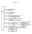
- Fig. 2 is a block diagram of one processor constituting a multiprocessor system in accordance with an embodiment of the present invention
- Fig. 3 is a diagram of an example of the multiprocessor system constituted by a processor A and a processor B connected by a communication line 26.
- each processor has a register 20 for temporarily storing data or the result of calculation, and a memory 21 in which a program (including procedures shown in Figs. 10(a) and 10(b)) or data is stored.
- the program includes also a user program and an operating system. The operating system controls the execution of the user program.
- the program stored in the memory 21 is sent to an instruction decoder 22 through a bus 28 to be interpreted.
- the result of interpretation is sent to an instruction execution section 23 to be executed.
- the result of the execution through the bus 28 is one of the following operations or a combination of some of them:
- the external units 27a and 27b may be a keyboard and a display.
- Each of the instruction decoder 22 and the instruction execution section 23 is realized by using a matrix, AND/OR logic, wired logic or a microprogram.
- the communication controller 25 can be constituted of a serial communication control LSI device on the market and is provided with a command buffer and a flag.
- Each instruction has an instruction code 41 indicating the kind of the instruction, an auxiliary code 42 for assisting in sorting with the instruction code 41 and used to indicate, for example, the form of the operands.
- the rest of each instruction i.e., the third and other subsequent bytes are operands which are used to indicate the addresses of processing object data and other values.
- Examples of the operands shown in Fig. 4 are a first operand 43 and a second operand 44 each having a length of 2 bytes. However, the number of operands and the length of each operand vary according to the kind of instruction and are determined by the instruction code 41 and the auxiliary code 42.
- a Move instruction which is a data transfer instruction has a form such as that shown in Fig. 5.
- the auxiliary code represents addressing modes 52a and 52b
- the first operand represents source data 53 on a transfer source
- the second operand represents destination data 54 on a transfer destination.
- the addressing mode 52a indicates the form in which the source data 53 is expressed
- the addressing mode 52b indicates the form in which the destination data 54 is expressed.
- the examples of the source data 53 and the destination data 54 have a length of 2 bytes. However, the lengths of these categories of data vary according to the values of the addressing modes 52a and 52b.
- Figs. 6(a) to 6(c) show three kinds of data expression forms.
- Fig. 6(a) shows a data expression form in a direct mode using a processor ID for indicating which processor a variable exists on.
- Fig. 6(b) shows a data expression form in a direct mode using no processor ID, which is considered to indicate data on the processor receiving the corresponding instruction.
- Fig. 6(c) is a data expression form in an immediate mode, which has a value placed on the operand that is directly used as transfer object data.
- the mode shown in Fig. 6(a) is not used in the prior art, while the modes shown in Figs. 6(b) and 6(c) are ordinarily used as addressing modes of conventional computers. Needless to say, the immediate mode cannot be designated as a form for destination data on a transfer destination.
- Fig. 1 is a flow chart of the operation of the instruction decoder 22. It is assumed that, at the start of the operation shown in Fig. 1, the instruction code 41, the auxiliary code 42, the first operand 43 and the second operand 44 in the instruction have already been read from the memory 21 and input into an instruction buffer (not shown) provided in the instruction decoder. The following description reads with respect to the operation of the instruction decoder 22 on the processor A unless otherwise noted.
- Determination is made by the instruction decoder 22 as to whether the instruction fetched into the instruction buffer is a Move instruction. If NO, information for branching to step S16 is output.
- addressing modes 52a and 52b are referred to and the instruction decoder operates to examine whether source data 53 and destination data 54 exist on processor A or processor B. However, in the case of the immediate mode, the data is considered to exist on processor A. In the case of the direct mode using no processor ID, the data is considered to exist on the same processor as that receiving the instruction, i.e., processor A.
- step S13 If the source data is on the processor B, information for branching to step S13 is output.
- the instruction decoder 22 instructs the instruction execution section 23 to send a data transfer request command shown below to the processor B, thereby terminating the process.
- step S14 If the destination data is on the processor B, information for branching to step S14 is output.
- the instruction decoder 22 instructs the instruction execution section 23 to execute an inter-processor data transfer command shown below, thereby terminating the process.
- the instruction decoder 22 If both the source data and the destination data are on the other processor, i.e., processor B, the instruction decoder 22 outputs information to the instruction execution section 23 to perform error processing, since the multiprocessor system of this embodiment is not designed to cope with such a situation. The process is then terminated.
- the instruction decoder 22 instructs the instruction execution section 23 to perform ordinary processing in which there is no need to consider the other processor.
- the instruction execution section 23 sends an inter-processor communication command through the communication controller 25 in accordance with the instruction from the instruction decoder 22.
- the operation of the instruction decoder on the processor A is thus performed.
- the above procedure which may be realized by using a decoder as described above, may also be realized as a program control. In such a case, the procedure is stored in the memory 21 and executed by the processor.
- the instruction decoder on the processor B also checks the existence of data and requests for data transfer in the same manner.
- the form of inter-processor communication commands exchanged between the processors will be described below.
- the processors A and B exchange inter-processor communication commands in a form such as that shown in Fig. 7.
- Each command has a command code 71 indicating the kind of the command, and number 72 representing the number of bytes of operands provided on the third and other subsequent bytes. The number of operands and the length of each operand vary with respect to commands.
- Fig. 8 shows the form of the inter-processor data transfer request command used in step S13
- Fig. 9 shows the form of the inter-processor data transfer command used in step S14.
- the form shown in Fig. 8 includes a code 81 for the inter-processor data transfer request command and the number 82 of bytes of operands provided on the third and other subsequent bytes.
- the number of bytes of operands is 8.
- a first operand has a length of 4 bytes and consists of a processor ID 83 for the processor having source data and an address 84 of the source data.
- a second operand has a length of 4 bytes and consists of a processor ID 85 of the processor having destination data and an address 86 of the destination data.
- the processor ID 83 of the processor having source data is the processor ID of the processor B
- the processor ID 85 of the processor having destination data is the processor ID of the processor A.
- the form shown in Fig. 9 includes a code 91 of the inter-processor data transfer command and the number 92 of bytes of operands provided on the third and other subsequent bytes.
- the number of bytes of operands is 4.
- a first operand has a length of 2 bytes and consists of values 93 of source data.
- a second operand has a length of 2 bytes and consists of an address 94 of destination data.
- the procedure of inter-processor communication command processing will be described below.
- the inter-processor communication command processing is conducted based on a command reception interruption process shown in Fig. 10(a) and an inter-processor communication command processing section of the operating system shown in Fig. 10(b).
- the processors A and B receive an inter-processor communication command through the communication line 26, they start executing the command reception interruption processing program shown in Fig. 10(a) by a command reception interruption effected by the communication controller 25.
- the procedure of the command reception interruption processing program is as described below.
- step S21 command code 91 is fetched into the command buffer (not shown).
- step S22 the number 92 of bytes of operands is fetched in the command buffer and the processor A checks the command buffer.
- step S23 operands having the number of bytes detected in step S22 are fetched.
- step S24 the command reception flag (not shown) is turned on and the process is terminated.
- the command reception interruption program inhibits reception of inter-processor communication commands.
- the inter-processor command processing section of the operating system shown in Fig. 10(b) conducts actual processing when the command reception flag is turned on by the command reception interruption processing.
- the procedure of the inter-processor command processing will be described below.
- step S31 the command reception flag is checked. If it is OFF, the process branches off to step S36. If the command reception flag is ON, the process proceeds to step S32.
- step S32 the command code is read out of the command buffer and is analyzed.
- the process branches to step S33.
- the process branches to step S35.
- step S33 the processor ID of the processor having source data, the address of the source data, the processor ID of the processor having destination data, and the address of the destination data are read out as operands from the command reception buffer. Then, an inter-processor data transfer instruction in the form shown in Fig. 9 is formed. To create the values 93 of the source data, data in the address indicated by the address 84 of the source data which is one of the operands of the inter-processor data transfer request command is used. To create the address 94 of the destination data, the address 86 of the destination data which is one of the operands of the inter-processor data transfer request command is used.
- step S34 the inter-processor data transfer command formed in step S33 is sent to the processor having the destination data.
- step S35 in the case where the command is a data transfer command, the values of source data and the address of destination data are read out of the command reception buffer, and a data substitution operation for substituting the values of the source data in the destination data is performed.
- step S36 the command reception flag is turned off to prepare for the next command reception, and the process is terminated.
- processors there is no limit to the number of processors, although the above-described embodiment has only two processors.
- the present invention can easily be applied to a multiprocessor system having three or more processors interconnected by communication lines 26 as shown in Fig. 11(a) or 11(b).
- processor IDs designating the processors exist in operands of a data transfer instruction.
- processors can be discriminated by a method using no processor ID in which addresses of the memory are arranged so as to avoid overlapping with respect to other processors, and in which a processor discrimination procedure for conducting operations as shown in Fig. 12 is stored in memory 21 and is executed by the processors.
- the operation of the processor discrimination means shown in Fig. 12 will be described below, which is, in this case, provided in a multiprocessor system having three processors A, B, and C having memories arranged in address space as shown in Fig. 13. It is assumed here that before the execution of the operation of the processor discrimination means shown in Fig.
- operands of a data transfer instruction have been fetched and the addresses of source data and destination data have been separated, so that the address value can be compared with other data items. It is also assumed that the address of a variable X is indicated by an operand in this case.
- step 41 the address value is checked as to whether it is smaller than 4000H. If the address value is smaller than 4000H, the process branches to step S42. If the address value is equal to or greater than 4000H, the process branches to step S43.
- step S42 it is determined whether variable X exists on processor A.
- step S43 the address value is checked as to whether it is smaller than 8000H. If the address value is smaller than 8000H, the process branches to step S44. If the address value is equal to or greater than 8000H, the process branches to step S45.
- step S44 it is determined whether variable X exists on processor B.
- step S45 it is determined whether variable X exists on processor C.
- processors A to C can be discriminated even if there is no processor ID in the operands.
Landscapes
- Engineering & Computer Science (AREA)
- Computer Hardware Design (AREA)
- Theoretical Computer Science (AREA)
- Software Systems (AREA)
- Physics & Mathematics (AREA)
- General Engineering & Computer Science (AREA)
- General Physics & Mathematics (AREA)
- Multi Processors (AREA)
Claims (6)
- Système de traitement de l'information comportant une pluralité d'appareils de traitement de l'information interconnectés par des moyens de communication, le système de traitement de l'information étant caractérisé en ce que chacun de ladite pluralité d'appareils de traitement de l'information comprend:des moyens de discrimination (22, S12) pour référer à l'information sur une adresse de donnée source ou de donnée destination indiquée par un opérande d'une instruction de transfert de données à traiter dans chacun de ladite pluralité d'appareils de traitement de l'information, et pour discriminer celui desdits appareils de traitement de l'information auquel se rapporte la donnée source ou la donnée destination; etdes moyens de transfert (23, S13, S14, S15, S16) pour transférer une commande de requête de transfert de données par lesdits moyens de communication vers un appareil de traitement de l'information souhaité de ladite pluralité d'appareils de traitement de l'information en référant à l'adresse de la donnée source ou de la donnée destination indiquée par l'opérande de l'instruction de transfert de données sur la base du résultat de la discrimination effectuée par lesdits moyens de discrimination.
- Système de traitement de l'information selon la revendication 1, dans lequel lesdits moyens de transfert comportent des moyens pour transférer les données par lesdits moyens de communication.
- Système de traitement de l'information selon la revendication 1, dans lequel lesdits moyens de discrimination comportent des moyens pour discriminer les modes d'adressage.
- Appareil de traitement de l'information destiné à être utilisé dans un système de traitement de l'information comprenant une pluralité desdits appareils de traitement de l'information interconnectés par des moyens de communication, ledit appareil de traitement de l'information étant caractérisé par:des moyens de discrimination (22, S12) pour référer à l'information sur une adresse de donnée source ou de donnée destination indiquée par un opérande d'une instruction de transfert de données à traiter dans chacun de ladite pluralité d'appareils de traitement de l'information, et pour discriminer celui desdits appareils de traitement de l'information auquel se rapporte la donnée source ou la donnée destination; etdes moyens de transfert (23, S13, S14, S15, S16) pour transférer une commande de requête de transfert de données par lesdits moyens de communication vers un appareil de traitement de l'information souhaité de ladite pluralité d'appareils de traitement de l'information en référant à l'adresse de la donnée source ou de la donnée destination indiquée par l'opérande de l'instruction de transfert de données sur la base du résultat de la discrimination effectuée par lesdits moyens de discrimination.
- Appareil de traitement de l'information selon la revendication 4, dans lequel lesdits moyens de transfert comportent des moyens pour transférer les données par lesdits moyens de communication.
- Appareil de traitement de l'information selon la revendication 4, dans lequel lesdits moyens de discrimination comportent des moyens pour discriminer les modes d'adressage.
Applications Claiming Priority (2)
| Application Number | Priority Date | Filing Date | Title |
|---|---|---|---|
| JP271218/90 | 1990-10-08 | ||
| JP2271218A JPH04149658A (ja) | 1990-10-08 | 1990-10-08 | 情報処理装置 |
Publications (3)
| Publication Number | Publication Date |
|---|---|
| EP0480657A2 EP0480657A2 (fr) | 1992-04-15 |
| EP0480657A3 EP0480657A3 (en) | 1992-11-19 |
| EP0480657B1 true EP0480657B1 (fr) | 1998-08-12 |
Family
ID=17496997
Family Applications (1)
| Application Number | Title | Priority Date | Filing Date |
|---|---|---|---|
| EP91309171A Expired - Lifetime EP0480657B1 (fr) | 1990-10-08 | 1991-10-07 | Appareil traitant une information |
Country Status (4)
| Country | Link |
|---|---|
| US (1) | US5369746A (fr) |
| EP (1) | EP0480657B1 (fr) |
| JP (1) | JPH04149658A (fr) |
| DE (1) | DE69129962T2 (fr) |
Families Citing this family (6)
| Publication number | Priority date | Publication date | Assignee | Title |
|---|---|---|---|---|
| JPH0863346A (ja) * | 1994-08-25 | 1996-03-08 | Canon Inc | プログラム編集方法とその装置 |
| KR100414922B1 (ko) * | 1995-12-22 | 2004-03-27 | 삼성전자주식회사 | 통신 모듈의 보드 선택장치 |
| FR2746527B1 (fr) * | 1996-03-21 | 1998-05-07 | Suisse Electronique Microtech | Dispositif de traitement d'information comportant plusieurs processeurs en parallele |
| WO2002082258A2 (fr) * | 2001-03-30 | 2002-10-17 | Canon Kabushiki Kaisha | Procede de gestion de fichiers |
| JP2004072350A (ja) * | 2002-08-05 | 2004-03-04 | Canon Inc | デジタルカメラおよびプリンタ |
| JP4831599B2 (ja) | 2005-06-28 | 2011-12-07 | ルネサスエレクトロニクス株式会社 | 処理装置 |
Family Cites Families (6)
| Publication number | Priority date | Publication date | Assignee | Title |
|---|---|---|---|---|
| US3787891A (en) * | 1972-07-03 | 1974-01-22 | Ibm | Signal processor instruction for non-blocking communication between data processing units |
| JPH0638600B2 (ja) * | 1983-12-28 | 1994-05-18 | 株式会社東芝 | ローカルエリアネットワークシステム |
| AU589400B2 (en) * | 1985-03-05 | 1989-10-12 | Wang Laboratories, Inc. | Apparatus and method for control of one computer system by another computer system |
| DE3667214D1 (de) * | 1985-09-20 | 1990-01-04 | Siemens Ag | Multi-mikroprozessorsystem mit zeitsparender adressierung von schreib-lese-speichern. |
| EP0313668B1 (fr) * | 1987-05-06 | 1997-08-06 | Fujitsu Ten, Ltd. | Dispositif de transfert de donnees |
| KR920006617B1 (ko) * | 1988-06-07 | 1992-08-10 | 가부시기가이샤 히다찌세이사꾸쇼 | 멀티프로세서시스템 |
-
1990
- 1990-10-08 JP JP2271218A patent/JPH04149658A/ja active Pending
-
1991
- 1991-10-07 EP EP91309171A patent/EP0480657B1/fr not_active Expired - Lifetime
- 1991-10-07 DE DE69129962T patent/DE69129962T2/de not_active Expired - Fee Related
-
1993
- 1993-09-24 US US08/126,029 patent/US5369746A/en not_active Expired - Fee Related
Also Published As
| Publication number | Publication date |
|---|---|
| DE69129962T2 (de) | 1999-01-14 |
| EP0480657A3 (en) | 1992-11-19 |
| EP0480657A2 (fr) | 1992-04-15 |
| JPH04149658A (ja) | 1992-05-22 |
| US5369746A (en) | 1994-11-29 |
| DE69129962D1 (de) | 1998-09-17 |
Similar Documents
| Publication | Publication Date | Title |
|---|---|---|
| EP0586813B1 (fr) | Automate programmable avec des instructions macros en diagramme à échelle | |
| JP3884487B2 (ja) | コンピュータ装置の所定の周辺装置から外部のアプリケーションパッケージへ必要データを利用できるようにする方法およびデータ交換論理 | |
| US5129093A (en) | Method and apparatus for executing an operation request signal in a loosely coupled parallel computer having processor elements capable of updating memory contents and minimizing exclusive control of sharable distributed memories | |
| US4156910A (en) | Nested data structures in a data driven digital data processor | |
| US4942519A (en) | Coprocessor having a slave processor capable of checking address mapping | |
| US4628436A (en) | Digital controller | |
| EP0464615A2 (fr) | Micro-ordinateur équipé d'un appareil de commande DMA | |
| EP0198231A2 (fr) | Processeur de données avec commande et exécution des instructions en parallèle | |
| US4692861A (en) | Microcomputer with interprocess communication | |
| EP0387871A2 (fr) | Système de commande d'adresse pour mémoire étendue | |
| EP0480657B1 (fr) | Appareil traitant une information | |
| US20020099922A1 (en) | Data processing apparatus including a plurality of pipeline processing mechanisms in which memory access instructions are carried out in a memory access pipeline | |
| EP0139254A2 (fr) | Appareil et méthode pour un transfert direct de données de mémoire vers un dispositif périphérique et du dispositif périphérique vers la mémoire | |
| US4156909A (en) | Structured data files in a data driven digital data processor | |
| US6184904B1 (en) | Central processing unit for a process control system | |
| US6883080B1 (en) | Program executing apparatus and program development supporting apparatus | |
| US4814977A (en) | Apparatus and method for direct memory to peripheral and peripheral to memory data transfers | |
| EP0546354B1 (fr) | Système de communication interprocesseur et méthode pour un circuit de multiprocesseur | |
| US5721954A (en) | Intelligent SCSI-2/DMA processor | |
| EP0560393B1 (fr) | Microprocesseur et système de traitement de données avec ensemble de registres | |
| JP3107308B2 (ja) | 異種言語混在形プログラム処理コントローラ | |
| JP3328867B2 (ja) | マルチプロセッサ演算装置、および該装置を有するプログラマブルコントローラ | |
| JP2511146B2 (ja) | デ―タ処理装置 | |
| JP2622026B2 (ja) | 中央処理装置におけるレジスタ書込制御方式 | |
| US5680646A (en) | Input/output control system |
Legal Events
| Date | Code | Title | Description |
|---|---|---|---|
| PUAI | Public reference made under article 153(3) epc to a published international application that has entered the european phase |
Free format text: ORIGINAL CODE: 0009012 |
|
| AK | Designated contracting states |
Kind code of ref document: A2 Designated state(s): DE FR GB IT NL |
|
| PUAL | Search report despatched |
Free format text: ORIGINAL CODE: 0009013 |
|
| AK | Designated contracting states |
Kind code of ref document: A3 Designated state(s): DE FR GB IT NL |
|
| 17P | Request for examination filed |
Effective date: 19930426 |
|
| 17Q | First examination report despatched |
Effective date: 19940811 |
|
| GRAG | Despatch of communication of intention to grant |
Free format text: ORIGINAL CODE: EPIDOS AGRA |
|
| GRAG | Despatch of communication of intention to grant |
Free format text: ORIGINAL CODE: EPIDOS AGRA |
|
| GRAH | Despatch of communication of intention to grant a patent |
Free format text: ORIGINAL CODE: EPIDOS IGRA |
|
| GRAG | Despatch of communication of intention to grant |
Free format text: ORIGINAL CODE: EPIDOS AGRA |
|
| GRAH | Despatch of communication of intention to grant a patent |
Free format text: ORIGINAL CODE: EPIDOS IGRA |
|
| GRAH | Despatch of communication of intention to grant a patent |
Free format text: ORIGINAL CODE: EPIDOS IGRA |
|
| GRAA | (expected) grant |
Free format text: ORIGINAL CODE: 0009210 |
|
| AK | Designated contracting states |
Kind code of ref document: B1 Designated state(s): DE FR GB IT NL |
|
| REF | Corresponds to: |
Ref document number: 69129962 Country of ref document: DE Date of ref document: 19980917 |
|
| NLR4 | Nl: receipt of corrected translation in the netherlands language at the initiative of the proprietor of the patent | ||
| ET | Fr: translation filed | ||
| PLBE | No opposition filed within time limit |
Free format text: ORIGINAL CODE: 0009261 |
|
| STAA | Information on the status of an ep patent application or granted ep patent |
Free format text: STATUS: NO OPPOSITION FILED WITHIN TIME LIMIT |
|
| 26N | No opposition filed | ||
| REG | Reference to a national code |
Ref country code: GB Ref legal event code: IF02 |
|
| PGFP | Annual fee paid to national office [announced via postgrant information from national office to epo] |
Ref country code: GB Payment date: 20050923 Year of fee payment: 15 |
|
| PGFP | Annual fee paid to national office [announced via postgrant information from national office to epo] |
Ref country code: NL Payment date: 20051018 Year of fee payment: 15 |
|
| PGFP | Annual fee paid to national office [announced via postgrant information from national office to epo] |
Ref country code: FR Payment date: 20051027 Year of fee payment: 15 |
|
| PGFP | Annual fee paid to national office [announced via postgrant information from national office to epo] |
Ref country code: DE Payment date: 20051216 Year of fee payment: 15 |
|
| PGFP | Annual fee paid to national office [announced via postgrant information from national office to epo] |
Ref country code: IT Payment date: 20061031 Year of fee payment: 16 |
|
| PG25 | Lapsed in a contracting state [announced via postgrant information from national office to epo] |
Ref country code: DE Free format text: LAPSE BECAUSE OF NON-PAYMENT OF DUE FEES Effective date: 20070501 Ref country code: NL Free format text: LAPSE BECAUSE OF NON-PAYMENT OF DUE FEES Effective date: 20070501 |
|
| GBPC | Gb: european patent ceased through non-payment of renewal fee |
Effective date: 20061007 |
|
| NLV4 | Nl: lapsed or anulled due to non-payment of the annual fee |
Effective date: 20070501 |
|
| REG | Reference to a national code |
Ref country code: FR Ref legal event code: ST Effective date: 20070629 |
|
| PG25 | Lapsed in a contracting state [announced via postgrant information from national office to epo] |
Ref country code: GB Free format text: LAPSE BECAUSE OF NON-PAYMENT OF DUE FEES Effective date: 20061007 |
|
| PG25 | Lapsed in a contracting state [announced via postgrant information from national office to epo] |
Ref country code: FR Free format text: LAPSE BECAUSE OF NON-PAYMENT OF DUE FEES Effective date: 20061031 |
|
| PG25 | Lapsed in a contracting state [announced via postgrant information from national office to epo] |
Ref country code: IT Free format text: LAPSE BECAUSE OF NON-PAYMENT OF DUE FEES Effective date: 20071007 |