EP0481048B1 - Mikrowellenstrahler für zirkulare polarisation, frei von lötverbindung und schwebendem potential - Google Patents
Mikrowellenstrahler für zirkulare polarisation, frei von lötverbindung und schwebendem potential Download PDFInfo
- Publication number
- EP0481048B1 EP0481048B1 EP91908822A EP91908822A EP0481048B1 EP 0481048 B1 EP0481048 B1 EP 0481048B1 EP 91908822 A EP91908822 A EP 91908822A EP 91908822 A EP91908822 A EP 91908822A EP 0481048 B1 EP0481048 B1 EP 0481048B1
- Authority
- EP
- European Patent Office
- Prior art keywords
- layer
- patch element
- microstrip radiator
- radiator according
- welds
- Prior art date
- Legal status (The legal status is an assumption and is not a legal conclusion. Google has not performed a legal analysis and makes no representation as to the accuracy of the status listed.)
- Expired - Lifetime
Links
Images


Classifications
-
- H—ELECTRICITY
- H01—ELECTRIC ELEMENTS
- H01Q—ANTENNAS, i.e. RADIO AERIALS
- H01Q9/00—Electrically-short antennas having dimensions not more than twice the operating wavelength and consisting of conductive active radiating elements
- H01Q9/04—Resonant antennas
- H01Q9/16—Resonant antennas with feed intermediate between the extremities of the antenna, e.g. centre-fed dipole
- H01Q9/26—Resonant antennas with feed intermediate between the extremities of the antenna, e.g. centre-fed dipole with folded element or elements, the folded parts being spaced apart a small fraction of operating wavelength
- H01Q9/27—Spiral antennas
-
- H—ELECTRICITY
- H01—ELECTRIC ELEMENTS
- H01Q—ANTENNAS, i.e. RADIO AERIALS
- H01Q21/00—Antenna arrays or systems
- H01Q21/29—Combinations of different interacting antenna units for giving a desired directional characteristic
-
- H—ELECTRICITY
- H01—ELECTRIC ELEMENTS
- H01Q—ANTENNAS, i.e. RADIO AERIALS
- H01Q9/00—Electrically-short antennas having dimensions not more than twice the operating wavelength and consisting of conductive active radiating elements
- H01Q9/04—Resonant antennas
- H01Q9/0407—Substantially flat resonant element parallel to ground plane, e.g. patch antenna
- H01Q9/045—Substantially flat resonant element parallel to ground plane, e.g. patch antenna with particular feeding means
- H01Q9/0457—Substantially flat resonant element parallel to ground plane, e.g. patch antenna with particular feeding means electromagnetically coupled to the feed line
Definitions
- microstrip radiators in large alignments for use thereof in communication systems has been increasing little by little as new materials and new techniques appear, which aside from resolving problems, have notably cheapened the manufacturing processes.
- French Patent Application FR-A-2 122 341 disclose an oscillating circuit including a patch (12) and a diode (14), where the patch is coupled - without welds - to radiating spirals (15, 16).
- the oscillating circuit (12,14) a part of which (14) is formed integrally with the radiating elements (15,16), has to include welds necessary for connecting the diode (14) to the patch (12), the assembly will give rise to passive intermodulation products when used.
- German Patent Application DE-A-3 527 651 discloses a cavity backed antenna assembly with a radiating spiral (3).
- the German document does not indicate how to eliminate the passive intermodulation products induced by the welds that seem to be necessary in order to interconnect the different parts of the assembly.
- the radiator as claimed is supplied by electromagnetic coupling from a stripline and it is inlaid in the same structure of the feeding line.
- This radiator does not have welds, therefore there are no problems of PIMP's; and it does not contain isolated metallic masses of the conductors belonging to the feeding line, thus, it is free of electrostatic discharges.
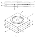
- Figure 1 shows a side view and top view of the device according to the present invention.
- Figure 2 shows the arrangement of the wires for the configuration of two feeding lines in the case of a circular slot.
- Figure 3 shows an alternative arrangement of the wires.
- Figure 4 shows two different radiation patterns.
- the radiator whose application is described, consists of three layers (10), (11) and (12), separated from each other by two dielectric materials (13) and (14.)
- the radiant surface (layer (10) in figure 1) consists of a metallic plane which contains the radiant element, which consists of a circular or square slot, with four wires (15) (existing in the photoetching mask itself,) which put in contact both edges of the slot.
- the metallic part of this plane, outside the radiant element, is one of the ground planes of the feeding stripline.
- the layer (11) contains the central strip of the stripline where the feeding circuit is, which can consist of two feeding lines to generate circular polarization as shown in figure 2, or else one line with the adequate disturbance.
- the layer (12) consists of a totally metallic plane and is one of the ground planes of the feeding stripline.
- Figure 2 shows the arrangement of the wires for the configuration of two feeding lines in the case of the radiator with circular geometry.
- This arrangement is similar to that of the 4 wire antenna cited in Nakano H., "Research on Spiral and Helical Antennas at Hosei University”, IEEE Antennas and Propagation Society Newsletter, June 1988.
- the operating of the antenna object of this patent can be reasoned as if the central metallic circle is a microstrip patch radiator which feeds a four wire antenna, providing the appropriate phases of excitation mode 1, according to the nomenclature cited in Nakano H., “Research on Spiral and Helical Antennas at Hosei University”, IEEE Antennas and Propagation Society Newsletter, June 1988.
- the overflow of the field itself of the patch makes the contribution to the four wire radiation rather smaller than that due to the microstrip patch, thus, the performance of the radiator object of this patent, would in such a case be very similar to the classic one of the microstrip patch radiator, slightly modifying the gain thereof and the height in the side lobes, when it is used in array.
- the axial ratio does not have the same performance when it is used in dual polarization, since an arrangement of wires like that shown in figure 3, improves the left-hand circular polarization of the microstrip patch and worsens the right-hand one, just as it is shown in figure 4, where the radiation patterns of two radiators, separated in both cases, are represented.
Landscapes
- Physics & Mathematics (AREA)
- Electromagnetism (AREA)
- Waveguide Aerials (AREA)
- Variable-Direction Aerials And Aerial Arrays (AREA)
- Details Of Aerials (AREA)
- Microwave Tubes (AREA)
Claims (8)
- Mikrostrip-Strahler für Zirkularpolarisation ohne Schweißstellen und Schwebepotentiale, wobei die Antenne auf einer Streifenleitung beruht, dadurch gekennzeichnet, daß er eine erste leitende Grundschicht (10) und eine zweite leitende Grundschicht (12) umfaßt;ein strahlendes Feldelement, das durch einen Schlitz von der ersten leitenden Grundschicht (10) getrennt ist;eine Drahtantenne, die wenigstens einen spiralförmigen Ring (15) umfaßt, der das Feldelement mit der ersten leitenden Grundschicht (10) verbindet;eine elektrische Eingangsschicht (11);einen Eingangsstreifen in der elektrischen Eingangsschicht (11), wobei der Eingangsstreifen unterhalb des Feldelementes endet;eine erste Schicht (13) aus dielektrischem Material, die die Eingangsschicht (11) von dem Feldelement trennt, wobei die erste Schicht (13) aus dielektrischem Material auch die Eingangsschicht (11) von der ersten leitenden Grundschicht (10) trennt;eine zweite Schicht (14) aus dielektrischem Material, die die zweite leitende Grundschicht (12) von der Eingangsschicht (11) trennt.
- Einen Mikrostrip-Strahler nach Anspruch 1, dadurch gekennzeichnet, daß der wenigstens eine spiralförmige Ring (15) auf einer zylindrischen Fläche angeordnet ist, wobei die Symmetrieachse parallel zur Senkrechten des Feldelementes ist.
- Mikrostrip-Strahler nach Anspruch 1, dadurch gekennzeichnet, daß der wenigstens eine spiralförmige Ring (15) auf einer konischen Fläche angeordnet ist, wobei die Symmetrieachse parallel zur Senkrechten des Feldelementes ist.
- Mikrostrip-Strahler nach einem der vorangehenden Ansprüche, dadurch gekennzeichnet, daß das Feldelement Kreisform hat.
- Mikrostrip-Strahler nach einem der Ansprüche 1-3, dadurch gekennzeichnet, daß das Feldelement quadratische Form hat.
- Mikrostrip-Strahler nach einem der vorangehenden Ansprüche, dadurch gekennzeichnet, daß die Drahtantenne vier spiralförmige Ringe (15) umfaßt.
- Mikrostrip-Strahler nach einem der Ansprüche 1-5, dadurch gekennzeichnet, daß er einen zusätzlichen Eingangsstreifen umfaßt, der vertikal unterhalb des Feldelementes endet.
- Mikrostrip-Strahler nach einem der vorangehenden Ansprüche, dadurch gekennzeichnet, daß die erste Schicht aus dielektrischem Material (13) in dem Bereich, in dem sich das Feldelement befindet, eine Dielektrizitätskonstante aufweist, die sich von der Dielektrizitätskonstante des restlichen Teils der ersten Schicht aus dielektrischem Material (13) unterscheidet.
Applications Claiming Priority (3)
| Application Number | Priority Date | Filing Date | Title |
|---|---|---|---|
| ES9001127A ES2021522A6 (es) | 1990-04-20 | 1990-04-20 | Radiador microbanda para polarizacion circular libre de soldaduras y potenciales flotantes. |
| ES9001127 | 1990-04-20 | ||
| PCT/ES1991/000024 WO1991017585A1 (es) | 1990-04-20 | 1991-04-19 | Radiador microbanda para polarizacion circular libre de soldaduras y potenciales flotantes |
Publications (2)
| Publication Number | Publication Date |
|---|---|
| EP0481048A1 EP0481048A1 (de) | 1992-04-22 |
| EP0481048B1 true EP0481048B1 (de) | 1996-04-03 |
Family
ID=8266966
Family Applications (1)
| Application Number | Title | Priority Date | Filing Date |
|---|---|---|---|
| EP91908822A Expired - Lifetime EP0481048B1 (de) | 1990-04-20 | 1991-04-19 | Mikrowellenstrahler für zirkulare polarisation, frei von lötverbindung und schwebendem potential |
Country Status (7)
| Country | Link |
|---|---|
| US (1) | US5353035A (de) |
| EP (1) | EP0481048B1 (de) |
| AT (1) | ATE136403T1 (de) |
| CA (1) | CA2063713C (de) |
| DE (1) | DE69118474T2 (de) |
| ES (2) | ES2021522A6 (de) |
| WO (1) | WO1991017585A1 (de) |
Families Citing this family (23)
| Publication number | Priority date | Publication date | Assignee | Title |
|---|---|---|---|---|
| US5668514A (en) * | 1994-10-12 | 1997-09-16 | Dai Nippon Printing Co., Ltd. | Signal transmission device |
| DE69434567T2 (de) * | 1994-10-12 | 2006-07-27 | Dai Nippon Printing Co., Ltd. | Signalübertragungseinrichtung unter Verwendung eines festen und eines drehbaren Körpers |
| JP3297601B2 (ja) * | 1996-04-25 | 2002-07-02 | 京セラ株式会社 | 複合アンテナ |
| US6025816A (en) * | 1996-12-24 | 2000-02-15 | Ericsson Inc. | Antenna system for dual mode satellite/cellular portable phone |
| USD416022S (en) | 1998-04-02 | 1999-11-02 | Lite-On Automotive Corp. | Microwave antenna |
| USD413329S (en) | 1999-02-02 | 1999-08-31 | Lite-On Automotive Corporation | Microwave antenna |
| DE19929879A1 (de) * | 1999-06-29 | 2001-01-18 | Bosch Gmbh Robert | Spiralantenne |
| US6480162B2 (en) * | 2000-01-12 | 2002-11-12 | Emag Technologies, Llc | Low cost compact omini-directional printed antenna |
| US6664932B2 (en) | 2000-01-12 | 2003-12-16 | Emag Technologies, Inc. | Multifunction antenna for wireless and telematic applications |
| MXPA02012930A (es) * | 2000-07-13 | 2003-10-14 | Thomson Licensing Sa | Antena plana de bandas multiples. |
| EP1831960B1 (de) * | 2004-12-27 | 2010-03-24 | Telefonaktiebolaget LM Ericsson (publ) | Dreifach polarisierte schlitzantenne |
| GB2447244A (en) * | 2007-03-06 | 2008-09-10 | Advanced Connection Tech Inc | Circularly polarized antenna with a radiating element surrounding a coupling element |
| JP5105208B2 (ja) * | 2007-05-17 | 2012-12-26 | 株式会社村田製作所 | アンテナ装置及び無線通信機 |
| US8629811B2 (en) * | 2011-09-15 | 2014-01-14 | The Charles Stark Draper Laboratory, Inc. | Dual band electrically small tunable antenna |
| US10971806B2 (en) | 2017-08-22 | 2021-04-06 | The Boeing Company | Broadband conformal antenna |
| US11233310B2 (en) * | 2018-01-29 | 2022-01-25 | The Boeing Company | Low-profile conformal antenna |
| US10916853B2 (en) | 2018-08-24 | 2021-02-09 | The Boeing Company | Conformal antenna with enhanced circular polarization |
| US10938082B2 (en) | 2018-08-24 | 2021-03-02 | The Boeing Company | Aperture-coupled microstrip-to-waveguide transitions |
| US10923831B2 (en) | 2018-08-24 | 2021-02-16 | The Boeing Company | Waveguide-fed planar antenna array with enhanced circular polarization |
| CN109888470B (zh) * | 2019-01-14 | 2023-12-15 | 华南理工大学 | 一种方向图分集的低剖面圆极化天线 |
| US11276933B2 (en) | 2019-11-06 | 2022-03-15 | The Boeing Company | High-gain antenna with cavity between feed line and ground plane |
| US11177548B1 (en) | 2020-05-04 | 2021-11-16 | The Boeing Company | Electromagnetic wave concentration |
| CN111984911B (zh) * | 2020-08-17 | 2023-11-14 | 西安电子科技大学 | 基于电磁对消的阵列天线辐射与散射综合优化方法 |
Family Cites Families (5)
| Publication number | Priority date | Publication date | Assignee | Title |
|---|---|---|---|---|
| FR1238355A (fr) * | 1959-06-30 | 1960-08-12 | Trt Telecom Radio Electr | Antenne pour véhicule aérien |
| FR2122341B1 (de) * | 1971-01-21 | 1974-04-26 | Radiotechnique Compelec | |
| US4063246A (en) * | 1976-06-01 | 1977-12-13 | Transco Products, Inc. | Coplanar stripline antenna |
| DE3527651A1 (de) * | 1985-08-01 | 1987-02-12 | Deutsche Forsch Luft Raumfahrt | Zusatzeinrichtung fuer eine antenne in form eines einzelstrahlers |
| US4879563A (en) * | 1987-10-30 | 1989-11-07 | Kyocera Corporation | Circularly polarized complementary antenna with patch and dipole elements |
-
1990
- 1990-04-20 ES ES9001127A patent/ES2021522A6/es not_active Expired - Lifetime
-
1991
- 1991-04-19 DE DE69118474T patent/DE69118474T2/de not_active Expired - Fee Related
- 1991-04-19 CA CA002063713A patent/CA2063713C/en not_active Expired - Fee Related
- 1991-04-19 EP EP91908822A patent/EP0481048B1/de not_active Expired - Lifetime
- 1991-04-19 WO PCT/ES1991/000024 patent/WO1991017585A1/es not_active Ceased
- 1991-04-19 ES ES91908822T patent/ES2088496T3/es not_active Expired - Lifetime
- 1991-04-19 AT AT91908822T patent/ATE136403T1/de not_active IP Right Cessation
-
1992
- 1992-01-17 US US07/833,832 patent/US5353035A/en not_active Expired - Fee Related
Also Published As
| Publication number | Publication date |
|---|---|
| EP0481048A1 (de) | 1992-04-22 |
| DE69118474T2 (de) | 1996-10-31 |
| ES2088496T3 (es) | 1996-08-16 |
| US5353035A (en) | 1994-10-04 |
| ATE136403T1 (de) | 1996-04-15 |
| ES2021522A6 (es) | 1991-11-01 |
| CA2063713C (en) | 1997-01-21 |
| DE69118474D1 (de) | 1996-05-09 |
| WO1991017585A1 (es) | 1991-11-14 |
Similar Documents
| Publication | Publication Date | Title |
|---|---|---|
| US5353035A (en) | Microstrip radiator for circular polarization free of welds and floating potentials | |
| JP3753436B2 (ja) | マルチバンドのプリント形モノポール・アンテナ | |
| US4063245A (en) | Microstrip antenna arrays | |
| Row et al. | Circular polarization and polarization reconfigurable designs for annular slot antennas | |
| US4197544A (en) | Windowed dual ground plane microstrip antennas | |
| US5990849A (en) | Compact spiral antenna | |
| US10944186B2 (en) | Antenna system and antenna module with reduced interference between radiating patterns | |
| US5208603A (en) | Frequency selective surface (FSS) | |
| US4291311A (en) | Dual ground plane microstrip antennas | |
| US6825816B2 (en) | Two-element and multi-element planar array antennas | |
| WO1996038882A9 (en) | Multiple band printed monopole antenna | |
| US6211839B1 (en) | Polarized planar log periodic antenna | |
| JP7539729B2 (ja) | アンテナ・イン・パッケージ及びレーダアセンブリパッケージ | |
| KR100198687B1 (ko) | 어레이 안테나 | |
| EP0450881A2 (de) | Mikrostreifenantennen | |
| CN114069216A (zh) | 圆极化天线和定位终端 | |
| US3488657A (en) | Low profile antenna | |
| EP3918671B1 (de) | Dualbandantenne mit gekerbter kreuzpolarisationsunterdrückung | |
| US9356353B1 (en) | Cog ring antenna for phased array applications | |
| Borah et al. | Design of a fan beam 1× 4 array antenna using V-shaped patch element for its use in X-band communication | |
| KR950007687B1 (ko) | 슬롯형 원형띠 안테나 | |
| JP3001276B2 (ja) | 薄形アンテナ | |
| JP2006287524A (ja) | 多周波平面アンテナ | |
| JPH04207505A (ja) | プリントアンテナ | |
| WO2001004992A1 (en) | Compact planar microstrip antenna |
Legal Events
| Date | Code | Title | Description |
|---|---|---|---|
| PUAI | Public reference made under article 153(3) epc to a published international application that has entered the european phase |
Free format text: ORIGINAL CODE: 0009012 |
|
| 17P | Request for examination filed |
Effective date: 19920115 |
|
| AK | Designated contracting states |
Kind code of ref document: A1 Designated state(s): AT BE CH DE DK ES FR GB GR IT LI LU NL SE |
|
| 17Q | First examination report despatched |
Effective date: 19940527 |
|
| GRAH | Despatch of communication of intention to grant a patent |
Free format text: ORIGINAL CODE: EPIDOS IGRA |
|
| GRAA | (expected) grant |
Free format text: ORIGINAL CODE: 0009210 |
|
| AK | Designated contracting states |
Kind code of ref document: B1 Designated state(s): AT BE CH DE DK ES FR GB GR IT LI LU NL SE |
|
| PG25 | Lapsed in a contracting state [announced via postgrant information from national office to epo] |
Ref country code: LI Free format text: LAPSE BECAUSE OF FAILURE TO SUBMIT A TRANSLATION OF THE DESCRIPTION OR TO PAY THE FEE WITHIN THE PRESCRIBED TIME-LIMIT Effective date: 19960403 Ref country code: GR Free format text: LAPSE BECAUSE OF FAILURE TO SUBMIT A TRANSLATION OF THE DESCRIPTION OR TO PAY THE FEE WITHIN THE PRESCRIBED TIME-LIMIT Effective date: 19960403 Ref country code: DK Effective date: 19960403 Ref country code: CH Free format text: LAPSE BECAUSE OF FAILURE TO SUBMIT A TRANSLATION OF THE DESCRIPTION OR TO PAY THE FEE WITHIN THE PRESCRIBED TIME-LIMIT Effective date: 19960403 Ref country code: BE Effective date: 19960403 Ref country code: AT Effective date: 19960403 |
|
| REF | Corresponds to: |
Ref document number: 136403 Country of ref document: AT Date of ref document: 19960415 Kind code of ref document: T |
|
| PG25 | Lapsed in a contracting state [announced via postgrant information from national office to epo] |
Ref country code: LU Free format text: LAPSE BECAUSE OF NON-PAYMENT OF DUE FEES Effective date: 19960430 |
|
| REF | Corresponds to: |
Ref document number: 69118474 Country of ref document: DE Date of ref document: 19960509 |
|
| ITF | It: translation for a ep patent filed | ||
| PG25 | Lapsed in a contracting state [announced via postgrant information from national office to epo] |
Ref country code: SE Effective date: 19960703 |
|
| ET | Fr: translation filed | ||
| REG | Reference to a national code |
Ref country code: CH Ref legal event code: PL |
|
| PLBE | No opposition filed within time limit |
Free format text: ORIGINAL CODE: 0009261 |
|
| STAA | Information on the status of an ep patent application or granted ep patent |
Free format text: STATUS: NO OPPOSITION FILED WITHIN TIME LIMIT |
|
| 26N | No opposition filed | ||
| REG | Reference to a national code |
Ref country code: GB Ref legal event code: IF02 |
|
| PGFP | Annual fee paid to national office [announced via postgrant information from national office to epo] |
Ref country code: GB Payment date: 20020417 Year of fee payment: 12 |
|
| PGFP | Annual fee paid to national office [announced via postgrant information from national office to epo] |
Ref country code: NL Payment date: 20020426 Year of fee payment: 12 Ref country code: FR Payment date: 20020426 Year of fee payment: 12 |
|
| PGFP | Annual fee paid to national office [announced via postgrant information from national office to epo] |
Ref country code: DE Payment date: 20020531 Year of fee payment: 12 |
|
| PG25 | Lapsed in a contracting state [announced via postgrant information from national office to epo] |
Ref country code: GB Free format text: LAPSE BECAUSE OF NON-PAYMENT OF DUE FEES Effective date: 20030419 |
|
| PGFP | Annual fee paid to national office [announced via postgrant information from national office to epo] |
Ref country code: ES Payment date: 20030430 Year of fee payment: 13 |
|
| PG25 | Lapsed in a contracting state [announced via postgrant information from national office to epo] |
Ref country code: NL Free format text: LAPSE BECAUSE OF NON-PAYMENT OF DUE FEES Effective date: 20031101 Ref country code: DE Free format text: LAPSE BECAUSE OF NON-PAYMENT OF DUE FEES Effective date: 20031101 |
|
| NLV4 | Nl: lapsed or anulled due to non-payment of the annual fee |
Effective date: 20031101 |
|
| GBPC | Gb: european patent ceased through non-payment of renewal fee |
Effective date: 20030419 |
|
| PG25 | Lapsed in a contracting state [announced via postgrant information from national office to epo] |
Ref country code: FR Free format text: LAPSE BECAUSE OF NON-PAYMENT OF DUE FEES Effective date: 20031231 |
|
| REG | Reference to a national code |
Ref country code: FR Ref legal event code: ST |
|
| PG25 | Lapsed in a contracting state [announced via postgrant information from national office to epo] |
Ref country code: ES Free format text: LAPSE BECAUSE OF NON-PAYMENT OF DUE FEES Effective date: 20040420 |
|
| PG25 | Lapsed in a contracting state [announced via postgrant information from national office to epo] |
Ref country code: IT Free format text: LAPSE BECAUSE OF NON-PAYMENT OF DUE FEES Effective date: 20050419 |
|
| REG | Reference to a national code |
Ref country code: ES Ref legal event code: FD2A Effective date: 20040420 |