EP0481706A1 - Erzeugungsmethode einer CVD-Silizium-Oxynitridschicht - Google Patents
Erzeugungsmethode einer CVD-Silizium-Oxynitridschicht Download PDFInfo
- Publication number
- EP0481706A1 EP0481706A1 EP91309441A EP91309441A EP0481706A1 EP 0481706 A1 EP0481706 A1 EP 0481706A1 EP 91309441 A EP91309441 A EP 91309441A EP 91309441 A EP91309441 A EP 91309441A EP 0481706 A1 EP0481706 A1 EP 0481706A1
- Authority
- EP
- European Patent Office
- Prior art keywords
- gas
- reaction vessel
- silicon oxynitride
- containing organic
- nitrogen containing
- Prior art date
- Legal status (The legal status is an assumption and is not a legal conclusion. Google has not performed a legal analysis and makes no representation as to the accuracy of the status listed.)
- Granted
Links
Images
Classifications
-
- H—ELECTRICITY
- H10—SEMICONDUCTOR DEVICES; ELECTRIC SOLID-STATE DEVICES NOT OTHERWISE PROVIDED FOR
- H10P—GENERIC PROCESSES OR APPARATUS FOR THE MANUFACTURE OR TREATMENT OF DEVICES COVERED BY CLASS H10
- H10P14/00—Formation of materials, e.g. in the shape of layers or pillars
- H10P14/60—Formation of materials, e.g. in the shape of layers or pillars of insulating materials
- H10P14/66—Formation of materials, e.g. in the shape of layers or pillars of insulating materials characterised by the type of materials
- H10P14/668—Formation of materials, e.g. in the shape of layers or pillars of insulating materials characterised by the type of materials the materials being characterised by the deposition precursor materials
- H10P14/6681—Formation of materials, e.g. in the shape of layers or pillars of insulating materials characterised by the type of materials the materials being characterised by the deposition precursor materials the precursor containing a compound comprising Si
- H10P14/6682—Formation of materials, e.g. in the shape of layers or pillars of insulating materials characterised by the type of materials the materials being characterised by the deposition precursor materials the precursor containing a compound comprising Si the compound being a silane, e.g. disilane, methylsilane or chlorosilane
-
- H—ELECTRICITY
- H10—SEMICONDUCTOR DEVICES; ELECTRIC SOLID-STATE DEVICES NOT OTHERWISE PROVIDED FOR
- H10P—GENERIC PROCESSES OR APPARATUS FOR THE MANUFACTURE OR TREATMENT OF DEVICES COVERED BY CLASS H10
- H10P14/00—Formation of materials, e.g. in the shape of layers or pillars
- H10P14/60—Formation of materials, e.g. in the shape of layers or pillars of insulating materials
- H10P14/69—Inorganic materials
- H10P14/692—Inorganic materials composed of oxides, glassy oxides or oxide-based glasses
- H10P14/6921—Inorganic materials composed of oxides, glassy oxides or oxide-based glasses containing silicon
- H10P14/6922—Inorganic materials composed of oxides, glassy oxides or oxide-based glasses containing silicon the material containing Si, O and at least one of H, N, C, F or other non-metal elements, e.g. SiOC, SiOC:H or SiONC
- H10P14/6927—Inorganic materials composed of oxides, glassy oxides or oxide-based glasses containing silicon the material containing Si, O and at least one of H, N, C, F or other non-metal elements, e.g. SiOC, SiOC:H or SiONC the material being a silicon oxynitride, e.g. SiON or SiON:H
-
- C—CHEMISTRY; METALLURGY
- C23—COATING METALLIC MATERIAL; COATING MATERIAL WITH METALLIC MATERIAL; CHEMICAL SURFACE TREATMENT; DIFFUSION TREATMENT OF METALLIC MATERIAL; COATING BY VACUUM EVAPORATION, BY SPUTTERING, BY ION IMPLANTATION OR BY CHEMICAL VAPOUR DEPOSITION, IN GENERAL; INHIBITING CORROSION OF METALLIC MATERIAL OR INCRUSTATION IN GENERAL
- C23C—COATING METALLIC MATERIAL; COATING MATERIAL WITH METALLIC MATERIAL; SURFACE TREATMENT OF METALLIC MATERIAL BY DIFFUSION INTO THE SURFACE, BY CHEMICAL CONVERSION OR SUBSTITUTION; COATING BY VACUUM EVAPORATION, BY SPUTTERING, BY ION IMPLANTATION OR BY CHEMICAL VAPOUR DEPOSITION, IN GENERAL
- C23C16/00—Chemical coating by decomposition of gaseous compounds, without leaving reaction products of surface material in the coating, i.e. chemical vapour deposition [CVD] processes
- C23C16/22—Chemical coating by decomposition of gaseous compounds, without leaving reaction products of surface material in the coating, i.e. chemical vapour deposition [CVD] processes characterised by the deposition of inorganic material, other than metallic material
- C23C16/30—Deposition of compounds, mixtures or solid solutions, e.g. borides, carbides, nitrides
- C23C16/308—Oxynitrides
-
- H—ELECTRICITY
- H10—SEMICONDUCTOR DEVICES; ELECTRIC SOLID-STATE DEVICES NOT OTHERWISE PROVIDED FOR
- H10P—GENERIC PROCESSES OR APPARATUS FOR THE MANUFACTURE OR TREATMENT OF DEVICES COVERED BY CLASS H10
- H10P14/00—Formation of materials, e.g. in the shape of layers or pillars
- H10P14/60—Formation of materials, e.g. in the shape of layers or pillars of insulating materials
- H10P14/63—Formation of materials, e.g. in the shape of layers or pillars of insulating materials characterised by the formation processes
- H10P14/6326—Deposition processes
- H10P14/6328—Deposition from the gas or vapour phase
- H10P14/6334—Deposition from the gas or vapour phase using decomposition or reaction of gaseous or vapour phase compounds, i.e. chemical vapour deposition
- H10P14/6336—Deposition from the gas or vapour phase using decomposition or reaction of gaseous or vapour phase compounds, i.e. chemical vapour deposition in the presence of a plasma [PECVD]
-
- H—ELECTRICITY
- H10—SEMICONDUCTOR DEVICES; ELECTRIC SOLID-STATE DEVICES NOT OTHERWISE PROVIDED FOR
- H10P—GENERIC PROCESSES OR APPARATUS FOR THE MANUFACTURE OR TREATMENT OF DEVICES COVERED BY CLASS H10
- H10P14/00—Formation of materials, e.g. in the shape of layers or pillars
- H10P14/60—Formation of materials, e.g. in the shape of layers or pillars of insulating materials
- H10P14/66—Formation of materials, e.g. in the shape of layers or pillars of insulating materials characterised by the type of materials
- H10P14/668—Formation of materials, e.g. in the shape of layers or pillars of insulating materials characterised by the type of materials the materials being characterised by the deposition precursor materials
- H10P14/6681—Formation of materials, e.g. in the shape of layers or pillars of insulating materials characterised by the type of materials the materials being characterised by the deposition precursor materials the precursor containing a compound comprising Si
- H10P14/6687—Formation of materials, e.g. in the shape of layers or pillars of insulating materials characterised by the type of materials the materials being characterised by the deposition precursor materials the precursor containing a compound comprising Si the compound comprising silicon and nitrogen
- H10P14/6689—Formation of materials, e.g. in the shape of layers or pillars of insulating materials characterised by the type of materials the materials being characterised by the deposition precursor materials the precursor containing a compound comprising Si the compound comprising silicon and nitrogen the compound being a silazane
-
- H—ELECTRICITY
- H10—SEMICONDUCTOR DEVICES; ELECTRIC SOLID-STATE DEVICES NOT OTHERWISE PROVIDED FOR
- H10P—GENERIC PROCESSES OR APPARATUS FOR THE MANUFACTURE OR TREATMENT OF DEVICES COVERED BY CLASS H10
- H10P14/00—Formation of materials, e.g. in the shape of layers or pillars
- H10P14/60—Formation of materials, e.g. in the shape of layers or pillars of insulating materials
- H10P14/69—Inorganic materials
- H10P14/694—Inorganic materials composed of nitrides
- H10P14/6943—Inorganic materials composed of nitrides containing silicon
- H10P14/69433—Inorganic materials composed of nitrides containing silicon the material being a silicon nitride not containing oxygen, e.g. SixNy or SixByNz
Definitions
- the present invention generally relates to a method of producing an insulating film for use as an insulating film provided on a semiconductor substrate, interlayer insulating film and an outermost passivation film of a semiconductor device, and more particularly to a method of producing a CVD silicon oxynitride (SiON) film.
- SiON silicon oxynitride
- insulating films are used. For instance, an interlayer insulating film is arranged between metal layers and a passivation film is provided on an outermost surface of a semiconductor device.
- insulating films are formed by silicon oxide (SiO2), phosphosilicate glass (PSG), borophosphosilicate glass (BPSG), silicon nitride (Si3N4), and silicon oxynitride (SiON).
- the silicon oxide, phosphosilicate glass and borophosphosilicate glass have a small dielectric constant and superior insulating property, but have poor wet-proof property. Silicon nitride has a superior wet-proof, but its dielectric constant is high.
- Silicon oxynitride has intermediate characteristics between silicon oxide and silicon nitride, so that it is possible to obtain an insulating film which has superior wet-proof and insulating property as well as a low dielectric constant by suitably selecting its composition. Due to this, many attempts and proposals have been done for utilizing the silicon oxynitride film as the protecting passivation film and insulating interlayer film in the semiconductor device.
- a mixture of mono-silane (SiH4), nitrous oxide (N2O) and ammonia (NH3) is introduced into a reaction vessel and the silicon oxynitride film is deposited on a semiconductor wafer by the plasma CVD.
- a main composition of the reaction gas i.e. mono-silane is poisonous, so that its treatment is cumbersome and the safety is required.
- a surface of a semiconductor wafer is exposed to a plasma gas and might be damaged by high energy electrons and charged particles. Due to this, electrical properties of the semiconductor device might be deteriorated and damaged and the manufacturing yield might be decreased.
- a mixture of an organic oxy silane gas and an ammonia gas is introduced into a reaction vessel which is kept at a low pressure such as 0.5 to 1.5 Torr, while a semiconductor wafer is heated at a relatively high temperature such as 750 to 800°C.
- a metal wiring conductor is usually formed by aluminum whose softening temperature is about 450°C, so that this known method could not be applied to the semiconductor devices comprising the aluminum wiring pattern.
- the reduced pressure is utilized, the step coverage is poor and it is rather difficult to obtain an insulating film having a flat surface.
- the mixture mainly consisting of the organic silane such as tetra ethoxy silane (TEOS) and the ammonia or nitrogen gas is utilized, so that the deposited silicon oxynitride film has hardly a desired composition.
- the present invention has for its object to provide a novel and useful method of producing a silicon oxynitride film having a desired composition safely without using the poisonous mono-silane, while the substrate is not heated at a temperature at which the aluminum wiring pattern is not softened.
- a method of producing an insulating film made of silicon oxynitride on a semiconductor substrate comprises the steps of: placing the semiconductor substrate in a reaction vessel; heating said semiconductor substrate at temperature not higher than 450°C; and introducing a mixture of a nitrogen containing organic silane gas and an ozone gas into the reaction vessel to perform a low temperature chemical vapour deposition.
- the reaction vessel is kept at the atmospheric pressure.
- the mixture of the nitrogen containing silane gas and the ozone gas is used as the reaction gas and it is no more necessary to use the poisonous mono-silane so that the method can be performed safely.
- the silicon oxynitride film is formed at the temperature not higher than 450°C, and therefore the metal wiring pattern formed on the substrate is not damaged. Therefore, the silicon oxynitride film formed by the method according to the invention could be advantageously used as the interlayer insulating film as well as the outermost protecting passivation film of the semiconductor wafer. Since the decomposition of the ozone gas occurs at a temperature not lower than 150°C, it is preferable to heat the semiconductor substrate at a temperature not lower than 150°C.
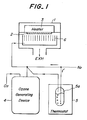
- Fig. 1 is a schematic view showing an embodiment of an apparatus for carrying out the method of producing the silicon oxynitride film according to the invention.
- the apparatus comprises a reaction vessel 1 and an electric heater 3 provided in the reaction vessel 1.
- a silicon wafer 2 is installed in the reaction vessel 1 and is heated at a desired temperature.
- the apparatus further comprises an ozone generating device 4 and a thermostat 5.
- a gas bubbler 5a which contains a nitrogen containing organic silicate material and through which a nitrogen gas is supplied to generate a nitrogen containing organic silane gas.
- a nitrogen gas is also used as a carrier gas.
- the carrier gas may be consisting of other inert gases such as Ar and He.
- the ozone gas generated by the ozone generating device 4, the nitrogen containing organic silane gas generated by the gas bubbler 5a in the thermostat 5 and the nitrogen carrier gas are supplied to the reaction vessel 1.
- the reaction vessel 1 there are further arranged vanes 6 for regulating the mixture gas so that a laminated gas stream can be projected against the silicon wafer 2.
- a mixture containing the ozone gas and the nitrogen containing organic silane gas (CH3)3SiNHSi(CH3)3 was introduced into the reaction vessel 1 and the pressure inside the reaction vessel was maintained at the atmospheric pressure.
- the nitrogen containing organic silane gas and the ozone gas were supplied at rates of 100 cc/min and 3 cc/min, respectively.
- the silicon wafer 2 was heated by the heater 3 at a temperature of 400°C. The deposition was performed for ten minutes.
- the temperature inside the reaction vessel 1 was about 370°C and the gas bubbler 5a arranged in the thermostat 5 was kept at a temperature of 100°C.
- the flow rate of O2 gas into the ozone generating device 4 was set to 4 liters per minute, the flow rate of the nitrogen gas into the gas bubbler 5a in the thermostat 5 was set to 1 liter per minute, and the nitrogen gas flow rate into the reaction vessel 1 was set to 20 liters per minute.
- the ozone gas generating factor in the ozone generating device 4 was 5%. In this manner, on the silicon wafer surface there was formed a silicon oxynitride film having a thickness of about 7000 ⁇ .
- a silicon wafer in which MOS transistor including a gate having a length of 1 ⁇ m and a width of 20 ⁇ m was formed was placed in a low pressure CVD device and a mixture of a mono-silane gas and an ammonia gas was introduced into the reaction vessel.
- a high frequency electric power is supplied to the reaction space and the plasma vapour deposition was carried out to produce a silicon oxynitride film serving as a passivation film.
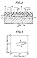
- the N-channel MOS transistors including the silicon oxynitride films formed by the method according to the invention and the known method were connected to bias voltage sources E1 and E2 as shown in Fig. 2.
- the transistor comprises a silicon substrate 11, source and drain regions 12 and 13 formed in the surface of the substrate 11, a gate oxide film 14, a polysilicon gate electrode 15, a BPSG film 16, aluminum electrodes 17, 18 and an insulating silicon oxynitride film 19.
- the gate has W/L of 20 ⁇ m/l ⁇ m.
- the source electrode 17 was connected to the ground potential and the drain electrode 18 was connected to a drain bias voltage source E1 of 7.5 V.
- the gate electrode 15 was connected to a gate bias voltage source E2 and the silicon substrate 11 was connected to the ground potential.
- the gate bias voltage source E2 was set to such a value that the substrate current I sub becomes maximum under the drain voltage of 2.0 V.
- the above mentioned bias condition was continued for 14 hours and the variation of the mutual conductance gm calculated from drain current (I D )/gate voltage (V G ) was monitored.
- Fig. 3 is a graph showing results of the above experiments.
- a horizontal axis denotes a stress time and a vertical axis represents the relative variation in the mutual conductance gm ( ⁇ gm/gm0).
- gm0 is an initial mutual conductance and ⁇ gm is a difference between a current mutual conductance and the initial mutual conductance.
- a curve A denotes the variation of the mutual conductance of the silicon oxynitride formed by the method according to the invention and a curve B represents the variation of the mutual conductance of the silicon oxynitride film formed by the known method.
- the decrease of the mutual conductance of the passivation film produced by the method according to the invention is smaller than that of the film formed by the known method.
- the substrate surface just below the gate is damaged by the ion bombardment and the substrate is charged up.
- the mutual conductance gm is calculated from I D /V G , and in the comparative example 1, the drain current I D is reduced due to the ion bombardment and charge-up of the substrate, so that the mutual conductance is decreased.
- the silicon oxynitride film is formed without using the plasma, and therefore the above explained damage and charge-up do not occur and the mutual conductance is not hardly decreased.
- the CVD is carried out under the atmospheric pressure, but according to the invention, it is also possible to produce the silicon oxynitride film by the high pressure CVD and the plasma CVD.
- the reaction vessel may be kept at a pressure such as 1.5 to 5 atm. Under the such a high pressure, a life time of the ozone is prolonged, and thus the deposition rate is increased and the flatness of the silicon oxynitride film is improved.
- the plasma CVD it is possible to obtain the silicon oxynitride film having the superior quality, but the flatness becomes worse.
- the mixture gas includes the nitrogen containing organic silane, the desired composition of the deposited silicon oxynitride film can be obtained.
- the silicon wafer may be vibrated in the reaction vessel.
- the reaction is performed at a temperature not higher than 450°C, the aluminum wiring conductors are not damaged during the CVD process, so that the silicon oxynitride is advantageously utilized as the outermost protecting passivation film of the semiconductor device.
- the process can be conducted easily by means of a simple apparatus. In the atmospheric pressure CVD and high pressure CVD, the substrate surface is not damaged by the plasma, and therefore the property of the semiconductor device is not deteriorated. Moreover, in the high pressure CVD, the deposition rate can be increased.
Landscapes
- Chemical & Material Sciences (AREA)
- Inorganic Chemistry (AREA)
- General Chemical & Material Sciences (AREA)
- Chemical Kinetics & Catalysis (AREA)
- Engineering & Computer Science (AREA)
- Materials Engineering (AREA)
- Mechanical Engineering (AREA)
- Metallurgy (AREA)
- Organic Chemistry (AREA)
- Formation Of Insulating Films (AREA)
Applications Claiming Priority (2)
| Application Number | Priority Date | Filing Date | Title |
|---|---|---|---|
| JP275264/90 | 1990-10-16 | ||
| JP2275264A JPH04151839A (ja) | 1990-10-16 | 1990-10-16 | シリコンオキシナイトライド膜の製造方法 |
Publications (2)
| Publication Number | Publication Date |
|---|---|
| EP0481706A1 true EP0481706A1 (de) | 1992-04-22 |
| EP0481706B1 EP0481706B1 (de) | 1995-04-12 |
Family
ID=17552996
Family Applications (1)
| Application Number | Title | Priority Date | Filing Date |
|---|---|---|---|
| EP91309441A Expired - Lifetime EP0481706B1 (de) | 1990-10-16 | 1991-10-15 | Erzeugungsmethode einer CVD-Silizium-Oxynitridschicht |
Country Status (5)
| Country | Link |
|---|---|
| EP (1) | EP0481706B1 (de) |
| JP (1) | JPH04151839A (de) |
| KR (1) | KR920008876A (de) |
| CA (1) | CA2053419A1 (de) |
| DE (1) | DE69108837T2 (de) |
Cited By (11)
| Publication number | Priority date | Publication date | Assignee | Title |
|---|---|---|---|---|
| DE4333160A1 (de) * | 1993-09-29 | 1995-03-30 | Siemens Ag | Herstellverfahren für eine nitridierte Siliziumoxidschicht mit verringerter Temperaturbelastung |
| EP0964441A3 (de) * | 1998-06-11 | 2000-03-15 | Air Products And Chemicals, Inc. | Ablagerung von Siliziumdioxid und Siliziumoxynitrid unter Gebrauch von Bis(tertiärbutylamino)silan |
| US7060614B2 (en) * | 2000-07-28 | 2006-06-13 | Tokyo Electron Limited | Method for forming film |
| EP1464724A3 (de) * | 2003-04-05 | 2007-01-10 | Rohm and Haas Electronic Materials, L.L.C. | Metallorganische Verbindungen, geeignet zur Verwendung in Dampfphasenabscheidungsprozessen |
| EP1535321A4 (de) * | 2002-08-18 | 2009-05-27 | Asml Us Inc | Niedertemperaturablagerung von siliziumoxiden und oxinitriden |
| EP1860690A3 (de) * | 2006-05-23 | 2010-03-17 | Air Products and Chemicals, Inc. | Verfahren zur Herstellung von Siliciumoxidfolien aus Organoaminosilanvorläufern |
| DE19680529B4 (de) * | 1995-06-06 | 2010-11-04 | Advanced Micro Devices Inc., Austin | Verfahren zur Herstellung von Hochdruck-Silicium-oxynitrid (Oxynitrid)-Gate-Dielektrika für Metalloxid Halbleiter (MOS)-Vorrichtungen mit polykristallinen P+-Silicium (Polysilicium)-Gate-Elektroden |
| US7875556B2 (en) | 2005-05-16 | 2011-01-25 | Air Products And Chemicals, Inc. | Precursors for CVD silicon carbo-nitride and silicon nitride films |
| US8530361B2 (en) | 2006-05-23 | 2013-09-10 | Air Products And Chemicals, Inc. | Process for producing silicon and oxide films from organoaminosilane precursors |
| US8771807B2 (en) | 2011-05-24 | 2014-07-08 | Air Products And Chemicals, Inc. | Organoaminosilane precursors and methods for making and using same |
| US8912353B2 (en) | 2010-06-02 | 2014-12-16 | Air Products And Chemicals, Inc. | Organoaminosilane precursors and methods for depositing films comprising same |
Families Citing this family (2)
| Publication number | Priority date | Publication date | Assignee | Title |
|---|---|---|---|---|
| JP3432601B2 (ja) * | 1994-06-17 | 2003-08-04 | 東京エレクトロン株式会社 | 成膜方法 |
| JP4877687B2 (ja) * | 2000-07-28 | 2012-02-15 | 東京エレクトロン株式会社 | 成膜方法 |
Citations (2)
| Publication number | Priority date | Publication date | Assignee | Title |
|---|---|---|---|---|
| US4158717A (en) * | 1977-02-14 | 1979-06-19 | Varian Associates, Inc. | Silicon nitride film and method of deposition |
| US4992306A (en) * | 1990-02-01 | 1991-02-12 | Air Products Abd Chemicals, Inc. | Deposition of silicon dioxide and silicon oxynitride films using azidosilane sources |
-
1990
- 1990-10-16 JP JP2275264A patent/JPH04151839A/ja active Pending
-
1991
- 1991-10-15 CA CA002053419A patent/CA2053419A1/en not_active Abandoned
- 1991-10-15 EP EP91309441A patent/EP0481706B1/de not_active Expired - Lifetime
- 1991-10-15 DE DE69108837T patent/DE69108837T2/de not_active Expired - Fee Related
- 1991-10-16 KR KR1019910018202A patent/KR920008876A/ko not_active Withdrawn
Patent Citations (2)
| Publication number | Priority date | Publication date | Assignee | Title |
|---|---|---|---|---|
| US4158717A (en) * | 1977-02-14 | 1979-06-19 | Varian Associates, Inc. | Silicon nitride film and method of deposition |
| US4992306A (en) * | 1990-02-01 | 1991-02-12 | Air Products Abd Chemicals, Inc. | Deposition of silicon dioxide and silicon oxynitride films using azidosilane sources |
Non-Patent Citations (2)
| Title |
|---|
| PATENT ABSTRACTS OF JAPAN vol. 11, no. 81 (E-488)12 March 1987 & JP-A-61 234 534 ( SEMICONDUCTOR ENERGY LAB ) 18 October 1986 * |
| PATENT ABSTRACTS OF JAPAN vol. 13, no. 413 (E-820)12 September 1989 & JP-A-1 152 631 ( NEC ) 15 June 1989 * |
Cited By (21)
| Publication number | Priority date | Publication date | Assignee | Title |
|---|---|---|---|---|
| DE4333160A1 (de) * | 1993-09-29 | 1995-03-30 | Siemens Ag | Herstellverfahren für eine nitridierte Siliziumoxidschicht mit verringerter Temperaturbelastung |
| DE19680529B4 (de) * | 1995-06-06 | 2010-11-04 | Advanced Micro Devices Inc., Austin | Verfahren zur Herstellung von Hochdruck-Silicium-oxynitrid (Oxynitrid)-Gate-Dielektrika für Metalloxid Halbleiter (MOS)-Vorrichtungen mit polykristallinen P+-Silicium (Polysilicium)-Gate-Elektroden |
| EP0964441A3 (de) * | 1998-06-11 | 2000-03-15 | Air Products And Chemicals, Inc. | Ablagerung von Siliziumdioxid und Siliziumoxynitrid unter Gebrauch von Bis(tertiärbutylamino)silan |
| US7060614B2 (en) * | 2000-07-28 | 2006-06-13 | Tokyo Electron Limited | Method for forming film |
| EP1535321A4 (de) * | 2002-08-18 | 2009-05-27 | Asml Us Inc | Niedertemperaturablagerung von siliziumoxiden und oxinitriden |
| EP1464724A3 (de) * | 2003-04-05 | 2007-01-10 | Rohm and Haas Electronic Materials, L.L.C. | Metallorganische Verbindungen, geeignet zur Verwendung in Dampfphasenabscheidungsprozessen |
| US7413776B2 (en) | 2003-04-05 | 2008-08-19 | Rohm And Haas Electronic Materials Llc | Method of depositing a metal-containing film |
| US7767840B2 (en) | 2003-04-05 | 2010-08-03 | Rohm And Haas Electronic Materials Llc | Organometallic compounds |
| US9640386B2 (en) | 2005-05-16 | 2017-05-02 | Versum Materials Us, Llc | Precursors for CVD silicon carbo-nitride films |
| US7875556B2 (en) | 2005-05-16 | 2011-01-25 | Air Products And Chemicals, Inc. | Precursors for CVD silicon carbo-nitride and silicon nitride films |
| US8932675B2 (en) | 2005-05-16 | 2015-01-13 | Air Products And Chemicals, Inc. | Methods for depositing silicon carbo-nitride film |
| US7932413B2 (en) | 2005-05-16 | 2011-04-26 | Air Products And Chemicals, Inc. | Precursors for CVD silicon carbo-nitride films |
| US8383849B2 (en) | 2005-05-16 | 2013-02-26 | Air Products And Chemicals, Inc. | Precursors for CVD silicon carbo-nitride films |
| US7875312B2 (en) | 2006-05-23 | 2011-01-25 | Air Products And Chemicals, Inc. | Process for producing silicon oxide films for organoaminosilane precursors |
| EP2562797A1 (de) * | 2006-05-23 | 2013-02-27 | Air Products And Chemicals, Inc. | Verfahren zur Herstellung von Siliziumoxidschichten aus Organoaminosilanvorläuferverbindungen |
| US8530361B2 (en) | 2006-05-23 | 2013-09-10 | Air Products And Chemicals, Inc. | Process for producing silicon and oxide films from organoaminosilane precursors |
| EP2562798A1 (de) * | 2006-05-23 | 2013-02-27 | Air Products And Chemicals, Inc. | Verfahren zur Herstellung von Siliziumoxidschichten aus Organoaminosilanvorläuferverbindungen |
| US8940648B2 (en) | 2006-05-23 | 2015-01-27 | Air Products And Chemicals, Inc. | Process for producing silicon and oxide films from organoaminosilane precursors |
| EP1860690A3 (de) * | 2006-05-23 | 2010-03-17 | Air Products and Chemicals, Inc. | Verfahren zur Herstellung von Siliciumoxidfolien aus Organoaminosilanvorläufern |
| US8912353B2 (en) | 2010-06-02 | 2014-12-16 | Air Products And Chemicals, Inc. | Organoaminosilane precursors and methods for depositing films comprising same |
| US8771807B2 (en) | 2011-05-24 | 2014-07-08 | Air Products And Chemicals, Inc. | Organoaminosilane precursors and methods for making and using same |
Also Published As
| Publication number | Publication date |
|---|---|
| JPH04151839A (ja) | 1992-05-25 |
| KR920008876A (ko) | 1992-05-28 |
| CA2053419A1 (en) | 1992-04-17 |
| DE69108837D1 (de) | 1995-05-18 |
| DE69108837T2 (de) | 1995-08-24 |
| EP0481706B1 (de) | 1995-04-12 |
Similar Documents
| Publication | Publication Date | Title |
|---|---|---|
| US5314724A (en) | Process for forming silicon oxide film | |
| JP2699695B2 (ja) | 化学気相成長法 | |
| US7101815B2 (en) | Method for improving thickness uniformity of deposited ozone-TEOS silicate glass layers | |
| US5869149A (en) | Method for preparing nitrogen surface treated fluorine doped silicon dioxide films | |
| JP2596214B2 (ja) | 高純度薄膜の形成方法 | |
| US7312524B2 (en) | Method for fabricating an ultralow dielectric constant material as an intralevel or interlevel dielectric in a semiconductor device and electronic device made | |
| US5429995A (en) | Method of manufacturing silicon oxide film containing fluorine | |
| US5376591A (en) | Method for manufacturing semiconductor device | |
| US20080095951A1 (en) | Electron beam modification of cvd deposited low dielectric constant materials | |
| EP0573911A2 (de) | Verfahren zum Auftragen von Silizium-Oxid-Schichten mit verbesserten Eigenschaften | |
| EP0481706A1 (de) | Erzeugungsmethode einer CVD-Silizium-Oxynitridschicht | |
| US20030003243A1 (en) | Method for forming film | |
| JPH11233502A (ja) | 半導体上に酸化膜を形成する装置及び方法 | |
| US6413887B1 (en) | Method for producing silicon nitride series film | |
| EP0605980A2 (de) | Verfahren zur Ablagerung von Silizium-Nitrid und Silizium-Oxynitride schichten | |
| JPH05259156A (ja) | 半導体装置の製造方法 | |
| JPH07161705A (ja) | 半導体装置の多層配線層間絶縁膜の形成方法 | |
| US6432839B2 (en) | Film forming method and manufacturing method of semiconductor device | |
| JP3070894B2 (ja) | 薄膜形成方法 |
Legal Events
| Date | Code | Title | Description |
|---|---|---|---|
| PUAI | Public reference made under article 153(3) epc to a published international application that has entered the european phase |
Free format text: ORIGINAL CODE: 0009012 |
|
| AK | Designated contracting states |
Kind code of ref document: A1 Designated state(s): DE FR GB NL |
|
| 17P | Request for examination filed |
Effective date: 19920430 |
|
| 17Q | First examination report despatched |
Effective date: 19920623 |
|
| GRAA | (expected) grant |
Free format text: ORIGINAL CODE: 0009210 |
|
| AK | Designated contracting states |
Kind code of ref document: B1 Designated state(s): DE FR GB NL |
|
| PG25 | Lapsed in a contracting state [announced via postgrant information from national office to epo] |
Ref country code: NL Free format text: LAPSE BECAUSE OF NON-PAYMENT OF DUE FEES Effective date: 19950412 |
|
| ET | Fr: translation filed | ||
| REF | Corresponds to: |
Ref document number: 69108837 Country of ref document: DE Date of ref document: 19950518 |
|
| NLV1 | Nl: lapsed or annulled due to failure to fulfill the requirements of art. 29p and 29m of the patents act | ||
| PLBE | No opposition filed within time limit |
Free format text: ORIGINAL CODE: 0009261 |
|
| STAA | Information on the status of an ep patent application or granted ep patent |
Free format text: STATUS: NO OPPOSITION FILED WITHIN TIME LIMIT |
|
| 26N | No opposition filed | ||
| PGFP | Annual fee paid to national office [announced via postgrant information from national office to epo] |
Ref country code: FR Payment date: 20011010 Year of fee payment: 11 |
|
| PGFP | Annual fee paid to national office [announced via postgrant information from national office to epo] |
Ref country code: GB Payment date: 20011017 Year of fee payment: 11 |
|
| PGFP | Annual fee paid to national office [announced via postgrant information from national office to epo] |
Ref country code: DE Payment date: 20011029 Year of fee payment: 11 |
|
| REG | Reference to a national code |
Ref country code: GB Ref legal event code: IF02 |
|
| REG | Reference to a national code |
Ref country code: GB Ref legal event code: 732E |
|
| PG25 | Lapsed in a contracting state [announced via postgrant information from national office to epo] |
Ref country code: GB Free format text: LAPSE BECAUSE OF NON-PAYMENT OF DUE FEES Effective date: 20021015 |
|
| PG25 | Lapsed in a contracting state [announced via postgrant information from national office to epo] |
Ref country code: DE Free format text: LAPSE BECAUSE OF NON-PAYMENT OF DUE FEES Effective date: 20030501 |
|
| GBPC | Gb: european patent ceased through non-payment of renewal fee |
Effective date: 20021015 |
|
| PG25 | Lapsed in a contracting state [announced via postgrant information from national office to epo] |
Ref country code: FR Free format text: LAPSE BECAUSE OF NON-PAYMENT OF DUE FEES Effective date: 20030630 |
|
| REG | Reference to a national code |
Ref country code: FR Ref legal event code: ST |