EP0481747A1 - Méthode de formation d'image - Google Patents
Méthode de formation d'image Download PDFInfo
- Publication number
- EP0481747A1 EP0481747A1 EP91309516A EP91309516A EP0481747A1 EP 0481747 A1 EP0481747 A1 EP 0481747A1 EP 91309516 A EP91309516 A EP 91309516A EP 91309516 A EP91309516 A EP 91309516A EP 0481747 A1 EP0481747 A1 EP 0481747A1
- Authority
- EP
- European Patent Office
- Prior art keywords
- photoreceptor
- group
- layer
- carrier
- polycarbonate
- Prior art date
- Legal status (The legal status is an assumption and is not a legal conclusion. Google has not performed a legal analysis and makes no representation as to the accuracy of the status listed.)
- Granted
Links
Images

Classifications
-
- G—PHYSICS
- G03—PHOTOGRAPHY; CINEMATOGRAPHY; ANALOGOUS TECHNIQUES USING WAVES OTHER THAN OPTICAL WAVES; ELECTROGRAPHY; HOLOGRAPHY
- G03G—ELECTROGRAPHY; ELECTROPHOTOGRAPHY; MAGNETOGRAPHY
- G03G5/00—Recording-members for original recording by exposure, e.g. to light, to heat or to electrons; Manufacture thereof; Selection of materials therefor
- G03G5/02—Charge-receiving layers
- G03G5/04—Photoconductive layers; Charge-generation layers or charge-transporting layers; Additives therefor; Binders therefor
- G03G5/05—Organic bonding materials; Methods for coating a substrate with a photoconductive layer; Inert supplements for use in photoconductive layers
- G03G5/0528—Macromolecular bonding materials
- G03G5/0557—Macromolecular bonding materials obtained otherwise than by reactions only involving carbon-to-carbon unsatured bonds
- G03G5/0564—Polycarbonates
-
- G—PHYSICS
- G03—PHOTOGRAPHY; CINEMATOGRAPHY; ANALOGOUS TECHNIQUES USING WAVES OTHER THAN OPTICAL WAVES; ELECTROGRAPHY; HOLOGRAPHY
- G03G—ELECTROGRAPHY; ELECTROPHOTOGRAPHY; MAGNETOGRAPHY
- G03G13/00—Electrographic processes using a charge pattern
- G03G13/06—Developing
- G03G13/08—Developing using a solid developer, e.g. powder developer
- G03G13/09—Developing using a solid developer, e.g. powder developer using magnetic brush
-
- G—PHYSICS
- G03—PHOTOGRAPHY; CINEMATOGRAPHY; ANALOGOUS TECHNIQUES USING WAVES OTHER THAN OPTICAL WAVES; ELECTROGRAPHY; HOLOGRAPHY
- G03G—ELECTROGRAPHY; ELECTROPHOTOGRAPHY; MAGNETOGRAPHY
- G03G15/00—Apparatus for electrographic processes using a charge pattern
- G03G15/06—Apparatus for electrographic processes using a charge pattern for developing
- G03G15/08—Apparatus for electrographic processes using a charge pattern for developing using a solid developer, e.g. powder developer
- G03G15/09—Apparatus for electrographic processes using a charge pattern for developing using a solid developer, e.g. powder developer using magnetic brush
- G03G15/0921—Details concerning the magnetic brush roller structure, e.g. magnet configuration
-
- G—PHYSICS
- G03—PHOTOGRAPHY; CINEMATOGRAPHY; ANALOGOUS TECHNIQUES USING WAVES OTHER THAN OPTICAL WAVES; ELECTROGRAPHY; HOLOGRAPHY
- G03G—ELECTROGRAPHY; ELECTROPHOTOGRAPHY; MAGNETOGRAPHY
- G03G5/00—Recording-members for original recording by exposure, e.g. to light, to heat or to electrons; Manufacture thereof; Selection of materials therefor
- G03G5/14—Inert intermediate or cover layers for charge-receiving layers
- G03G5/147—Cover layers
- G03G5/14708—Cover layers comprising organic material
- G03G5/14713—Macromolecular material
- G03G5/14747—Macromolecular material obtained otherwise than by reactions only involving carbon-to-carbon unsaturated bonds
- G03G5/14756—Polycarbonates
Definitions
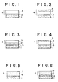
- Figures 1 through 6 are cross-sectional views showing the structural configuration of the photoreceptor of the present invention.
- Figure 7 is a schematic diagram of an image forming apparatus illustrating the method of image formation of the present invention.
- R1, R2, R3, R4, R5, R6, R7 and R8 independently represent a hydrogen atom, methyl group, chlorine atom or bromine atom, and not all the substituents are hydrogen atoms at the same time.
- R1 through R8 are synonymous with those as defined in Formula I, R9 or R10 represents a hydrogen atom or alkyl group having 1 to 6 carbon atoms.
- the magnetic flux density on the sleeve is kept at not less than 950 gauss to prevent the developing agent being transported on the sleeve from scattering and that a highly durable polycarbonate enduring such high speed copying has been selected as a binder resin to constitute the light-sensitive layer of the organic photoreceptor.
- the central carbon atom in the polycarbonate structure is involved in the formation of a ring by Z, which effectively prevents the molecular chain in the polycarbonate structure from orienting in a particular direction and hence prevents the crystallization and gelation of the polycarbonate.
- Z effectively prevents the molecular chain in the polycarbonate structure from orienting in a particular direction and hence prevents the crystallization and gelation of the polycarbonate.
- the resulting crystal or gel separates on, and protrudes from, the light-sensitive layer surface to cause an imaging failure.
- the light-sensitive layer surface is not liable to have flaws even in abrasion with magnetic brush or cleaning blade and high printability free of characteristic failures such as poor cleaning is obtained.
- Z forms a 5- or 6-membered carbon ring or heterocyclic ring, including a cyclohexyl ring and cyclopentyl ring, wherein a substituent such as an acetyl group or acetylamino group may have been introduced locally.
- an organic pigment such as a fluorenone dis-azo pigment, fluorenylidene dis-azo pigment, polycyclic quinone pigment, non-metallic phthalocyanine pigment or oxytitanyl phthalocyanine pigment as a carrier generation material in the photoreceptor for the present invention, with more preference given to the following fluorenone diazo pigment, fluorenylidene dis-azo pigment, polycyclic quinone pigment and X- and ⁇ -type non-metallic phthalocyanines, since they offer remarkable improvements in sensitivity, durability, image quality and other features.
- an organic pigment such as a fluorenone dis-azo pigment, fluorenylidene dis-azo pigment, polycyclic quinone pigment, non-metallic phthalocyanine pigment or oxytitanyl phthalocyanine pigment
- the dis-azo pigment of Formula 3 which serves well for the present invention is exemplified as the compounds represented by the following formulas, but these examples are not to be construed as limitative.
- the dibenzopyrenequinone pigment represented by Formula 5 is exemplified by the following compounds.
- the pyranthrone pigment represented by Formula 6 is exemplified by the following compounds.
- polycyclic quinones represented by Formulas 4 through 6 for the present invention can easily be synthesized by known methods.
- Ar5 and Ar6 independently represent a substituted or unsubstituted aryl group, the substituent being exemplified by an alkyl group, alkoxy group, substituted amino group, hydroxyl group, halogen atom and aryl group.
- R13 and R14 independently represent a substituted or unsubstituted aryl group or hydrogen atom, the substituent being exemplified by an alkyl group, alkoxy group, substituted amino group, hydroxyl group, halogen atom and aryl group.
- Examples of other useful carrier transport materials include those described in Japanese Patent O.P.I. Publication Nos. 64244/1982, 15252/1984, 67940/1982, 2285/1980, 195254/1982 and 4148/1981.
- the light-sensitive layer may contain one or more electron recipient substances.
- the light-sensitive layer for the present invention may contain an organic amine to improve the charge generation function of the carrier generation material, with preference given to a secondary amine.
- organic amine to improve the charge generation function of the carrier generation material, with preference given to a secondary amine.
- the photoreceptor for the present invention may contain as necessary an ultraviolet absorbent and other additives to protect the light-sensitive layer and also a color sensitivity correcting dye.
- the electroconductive support 1 which constitutes the photoreceptor for the present invention is prepared mainly from the following substances, but these are not to be construed as limitative.
- the carrier transport layer 3 is a layer wherein a carrier transport material as a main component is compatibly dissolved in a binder resin in a ratio of 0.1 to 5 parts by weight of the binder resin to 1 part by weight of the carrier transport material.
- the light-sensitive layer 4 of the photoreceptor for the present invention may be of a single layer structure.
- the thickness of the light-sensitive layer is 10 to 50 ⁇ m, preferably 15 to 40 ⁇ m, wherein 0.5 to 5 parts by weight of the carrier transport material and 0.5 to 10 parts by weight of the binder resin are contained per 1 part by weight of the carrier generation material.
- the photoreceptor for the present invention offers excellent electrophotographic performance with high durability and little fatigue deterioration when used for high speed repetitive transfer electrophotography.
- the developer used for the present invention is a two-component developer which is excellent in fluidity and frictional chargeability and hence in developability.
- the two-component developer preferably comprises a fine grains of non-magnetic toner and magnetic carrier grains.
- a low molecular polyolefin such as polypropylene, polyethylene or wax may be added to binder resin at 0 to 5 wt%.
- the carrier for the two-component developer for the present invention is capable of providing the desired charge for the toner.
- a magnetic material may be used as such, used after being coated with resin etc. or used as fine powder in mixture with resin, with preference given to a coated carrier prepared by coating a resin on the magnetic grain surface.
- the magnetic material examples include substances which magnetize very strongly in the direction of magnetic field, such as iron, cobalt, nickel and other metals, ferrite, magnetite, hematite and other alloys or compounds containing a ferromagnetic element such as iron, cobalt or nickel, and alloys which contain no ferromagnetic substance but which show ferromagnetism upon appropriate heat treatment such as Heusler's alloys containing manganese and copper (manganese-copper-aluminum alloy and manganese-copper-tin alloy) and chromium dioxide.
- substances which magnetize very strongly in the direction of magnetic field such as iron, cobalt, nickel and other metals, ferrite, magnetite, hematite and other alloys or compounds containing a ferromagnetic element such as iron, cobalt or nickel, and alloys which contain no ferromagnetic substance but which show ferromagnetism upon appropriate heat treatment
- the weight average grain diameter d of the carrier is normally 40 to 120 ⁇ m.
- the carrier resistivity is not less than 103 ⁇ -cm, preferably not less than 1013 ⁇ -cm, and still more preferably not less than 1014 ⁇ -cm for preventing charge injection into the carrier by bias voltage and subsequent adherence of the carrier on the image formation surface and leakage of bias voltage leading to elimination of the latent image charge.
- the two-component developer contains the carrier and toner in weight ratios of 98:2 to 85:15 and may contain as necessary a fluidizing agent such as hydrophobic silica, colloidal silica or silicon varnish and a cleaning aid such as a metal salt of fatty acid or fluorine surfactant in a ratio of 0.1 to 3 wt% of the toner.
- a fluidizing agent such as hydrophobic silica, colloidal silica or silicon varnish
- a cleaning aid such as a metal salt of fatty acid or fluorine surfactant in a ratio of 0.1 to 3 wt% of the toner.
- the original 10 on the original table 11 is scanned at a speed of X in the direction of arrow by the exposure system comprising the exposure lamps 12 and 13 and the reflective mirror 14a, which scanning light is reflected by the V mirrors 14b and 14c being running at a speed of X/2 and reaches the photoreceptor drum 20, pre-charged to 400 to 800 V by the charger 16 and rotating at a peripheral speed of not less than 300 mm/sec in the direction of arrow, via the image forming lens 15 and the reflective mirror 14d, on which photoreceptor drum imagewise exposure occurs and an electrostatic latent image forms.
- the peripheral speed of the sleeve 17a is set at 1 to 5 times the peripheral speed of the photoreceptor drum 20 (peripheral speed ratio K); therefore, as the copying speed increases, the peripheral speed of the sleeve 17a increases and carrier scattering becomes more likely to occur.
- the magnetic flux density on the sleeve is at least 950 gauss, preferably not more than 1200 gauss to ensure development free of carrier scattering.
- the iron powder grains mingled in the developer stand up as if they are magnetically attracted and cause abrasive deterioration of the surface of the photoreceptor during repeated image formation even when the photoreceptor has been improved according to the present invention.
- the peripheral speed of the photoreceptor preferably be under 600 mm/sec.
- the method of image formation described above makes it possible to stably forming a high quality image at high speed.
- a carrier generation material, carrier transport material, carrier generation layer and carrier transport layer are abbreviated CGM, CTM, CGL and CTL, respectively.
- a photoreceptor 2 was prepared in the same manner as in Example 1 except that the polycarbonate was replaced with a polymer comprising a homopolymer of the repeat unit of Exemplified Compound 1-2 and the CTM was Exemplified Compound 7-3.
- An interlayer was formed in the same manner as in Example 1. 20 g of a polycyclic quinone pigment (Exemplified Compound 4-3) as CGM and 10 g of a polycarbonate resin L-1250 (produced by Teijin Chemicals Ltd.) as a binder were dissolved in 1,2-dichloroethane (produced by Kanto Chemical Co., Ltd., special grade), followed by 24 hours of milling in a ball mill to yield a CGL coating solution, which was dip-coated on the interlayer to yield a 0.3 ⁇ m thick CGL.
- a polycyclic quinone pigment Exemplified Compound 4-3
- a polycarbonate resin L-1250 produced by Teijin Chemicals Ltd.
- 1,2-dichloroethane produced by Kanto Chemical Co., Ltd., special grade
- a photoreceptor 3 was prepared by CTL lamination in the same manner as in Example 1 except that the CTM was Exemplified Compound 7-5 and the binder resin was replaced with a polycarbonate (molecular weight 20000) comprising a homopolymer of the repeat unit of Exemplified Compound 1-3.
- Example 2 The resulting dispersion was dip-coated on the interlayer described in Example 1 to yield a CGL, followed by CTL formation in the same manner as in Example 2 to yield a photoreceptor 4.
- a photoreceptor (5) was prepared in the same manner as in Example 1 except that CTL binder was replaced with simple polycarbonate instead of examplified compound (1)-4 unit repeated polymer.
- a comparative photoreceptor 1 was prepared in the same manner as in Example 1 except that a bisphenol A polycarbonate (Panlite K-1300, produced by Teijin Chemicals Ltd.) was used as a CTL binder.
- a bisphenol A polycarbonate Panlite K-1300, produced by Teijin Chemicals Ltd.
- the sensitizing solution was found unstable, poor in retention stability and easily gelable during preparation of the photoreceptor.
- a comparative photoreceptor 2 was prepared in the same manner as in Example 1 except that a bisphenol Z polycarbonate (produced by Mitsubishi Gas Chemical Company, Inc.) was used as a CTL binder.
- Carbon black Mogal L (produced by Cabot) 10 parts by weight
- a polysiloxane having an ammonium salt functional group represented by the following formula was dissolved in xylene to yield a treating solution.
- X represents an integer.
- fine grains of silica Aerosil 200 (produced by Nihon Aerosil Co., Ltd.) were placed in a mixer and sprayed with the polysiloxane in a ratio such that the ratio of the polysiloxane was 5 wt%, after which they were transferred to a flask, followed by removing the solvent xylene while stirring at 200°C for 5 hours to yield inorganic fine grains surface treated with the polysiloxane having an ammonium salt functional group.
- ferrite grains F-150 produced by Nippon Teppun Kogyo
- a fluorine resin with the following structure to a film thickness of about 1.5 ⁇ m to yield a resin-coated carrier, which had a grain size of 80 ⁇ m.
- inventive photoreceptors 1 through 4 and comparative photoreceptors 1 and 2 were loaded on a version of U-BIX 5000 (produced by Konica Corporation), and the two-component developer was filled in the developing device of the copying machine, and the tests of Table 2 were conducted under the mechanical conditions shown in Table 1. Each test was repeated in 100000 cycles, and the surface potential of the photoreceptor was measured before and after actual imaging.
- Film wear due to friction on the photoreceptor surface was determined by measuring the film thickness of the photoreceptor after 100000 copies were taken and compared with the initial value.
- the image sample was sequentially checked by counting the copies with visible streaks or cleaning failures associated with flaws in the direction of the drum periphery.
- test samples according to the invention show little abrasive wear in the photoreceptor and little flaws or cleaning failures on the photoreceptor surface, while the comparative photoreceptors showed significant wear and deterioration.
- test samples according to the present invention showed little wear deterioration and electrophotographic performance degradation during repeated high speed copying, while the comparative samples showed significant wear deterioration in the photoreceptor.
Landscapes
- Physics & Mathematics (AREA)
- General Physics & Mathematics (AREA)
- Chemical & Material Sciences (AREA)
- Chemical Kinetics & Catalysis (AREA)
- Spectroscopy & Molecular Physics (AREA)
- Photoreceptors In Electrophotography (AREA)
Applications Claiming Priority (4)
| Application Number | Priority Date | Filing Date | Title |
|---|---|---|---|
| JP28091790A JPH04155366A (ja) | 1990-10-18 | 1990-10-18 | 画像形成方法 |
| JP280917/90 | 1990-10-18 | ||
| JP28091690A JPH04155365A (ja) | 1990-10-18 | 1990-10-18 | 画像形成方法 |
| JP280916/90 | 1990-10-18 |
Publications (2)
| Publication Number | Publication Date |
|---|---|
| EP0481747A1 true EP0481747A1 (fr) | 1992-04-22 |
| EP0481747B1 EP0481747B1 (fr) | 1998-01-07 |
Family
ID=26553982
Family Applications (1)
| Application Number | Title | Priority Date | Filing Date |
|---|---|---|---|
| EP19910309516 Expired - Lifetime EP0481747B1 (fr) | 1990-10-18 | 1991-10-16 | Méthode de formation d'image |
Country Status (2)
| Country | Link |
|---|---|
| EP (1) | EP0481747B1 (fr) |
| DE (1) | DE69128598T2 (fr) |
Citations (4)
| Publication number | Priority date | Publication date | Assignee | Title |
|---|---|---|---|---|
| US4800412A (en) * | 1985-03-22 | 1989-01-24 | Minolta Camera Kabushiki Kaisha | Apparatus for developing electrostatic latent images |
| GB2211954A (en) * | 1987-10-30 | 1989-07-12 | Konishiroku Photo Ind | Electrophotographic photoreceptor |
| DE3804449A1 (de) * | 1988-02-12 | 1989-08-24 | Konishiroku Photo Ind | Elektrophotographisches bilderzeugungsverfahren |
| EP0356246A2 (fr) * | 1988-08-25 | 1990-02-28 | Konica Corporation | Photorécepteur |
-
1991
- 1991-10-16 EP EP19910309516 patent/EP0481747B1/fr not_active Expired - Lifetime
- 1991-10-16 DE DE1991628598 patent/DE69128598T2/de not_active Expired - Lifetime
Patent Citations (4)
| Publication number | Priority date | Publication date | Assignee | Title |
|---|---|---|---|---|
| US4800412A (en) * | 1985-03-22 | 1989-01-24 | Minolta Camera Kabushiki Kaisha | Apparatus for developing electrostatic latent images |
| GB2211954A (en) * | 1987-10-30 | 1989-07-12 | Konishiroku Photo Ind | Electrophotographic photoreceptor |
| DE3804449A1 (de) * | 1988-02-12 | 1989-08-24 | Konishiroku Photo Ind | Elektrophotographisches bilderzeugungsverfahren |
| EP0356246A2 (fr) * | 1988-08-25 | 1990-02-28 | Konica Corporation | Photorécepteur |
Also Published As
| Publication number | Publication date |
|---|---|
| DE69128598T2 (de) | 2004-04-15 |
| EP0481747B1 (fr) | 1998-01-07 |
| DE69128598D1 (de) | 1998-02-12 |
Similar Documents
| Publication | Publication Date | Title |
|---|---|---|
| JP2001142235A (ja) | 電子写真用感光体 | |
| US20080187849A1 (en) | Electrophotographic apparatus | |
| JP3312179B2 (ja) | 電子写真感光体 | |
| JPS63159856A (ja) | 電子写真正帯電感光体及びその像形成プロセス | |
| EP0481747B1 (fr) | Méthode de formation d'image | |
| JPH0727227B2 (ja) | 電子写真感光体及び画像形成方法 | |
| JP2003302779A (ja) | 電子写真感光体、電子写真感光体の製造方法、画像形成方法、画像形成装置及びプロセスカートリッジ | |
| JPH0844096A (ja) | 電子写真感光体および電子写真装置 | |
| JP2003280223A (ja) | 有機感光体、画像形成方法、画像形成装置及びプロセスカートリッジ | |
| JPH0776838B2 (ja) | 電子写真感光体及び画像形成方法 | |
| JP2741449B2 (ja) | 電子写真感光体 | |
| JP2019139041A (ja) | 電子写真感光体及び電子写真画像形成装置 | |
| JPH0728255A (ja) | 電子写真感光体 | |
| JPH07209883A (ja) | 画像形成方法 | |
| JP2943393B2 (ja) | 電子写真用感光体およびその製造方法 | |
| JPH04155366A (ja) | 画像形成方法 | |
| JP2003307862A (ja) | 有機感光体、画像形成方法、画像形成装置及びプロセスカートリッジ | |
| JP2006126591A (ja) | カラー画像形成装置 | |
| JP3041704B2 (ja) | 画像形成法 | |
| JPH04155365A (ja) | 画像形成方法 | |
| JP2002040677A (ja) | 湿式現像方式の画像形成装置に使用される電子写真感光体 | |
| JPH07160013A (ja) | 画像形成方法 | |
| JPH01142640A (ja) | 電子写真用感光体 | |
| JPH07104526A (ja) | 画像形成方法 | |
| JPS63159858A (ja) | 電子写真感光体 |
Legal Events
| Date | Code | Title | Description |
|---|---|---|---|
| PUAI | Public reference made under article 153(3) epc to a published international application that has entered the european phase |
Free format text: ORIGINAL CODE: 0009012 |
|
| AK | Designated contracting states |
Kind code of ref document: A1 Designated state(s): DE GB |
|
| 17P | Request for examination filed |
Effective date: 19921001 |
|
| 17Q | First examination report despatched |
Effective date: 19960103 |
|
| GRAG | Despatch of communication of intention to grant |
Free format text: ORIGINAL CODE: EPIDOS AGRA |
|
| GRAG | Despatch of communication of intention to grant |
Free format text: ORIGINAL CODE: EPIDOS AGRA |
|
| GRAG | Despatch of communication of intention to grant |
Free format text: ORIGINAL CODE: EPIDOS AGRA |
|
| GRAH | Despatch of communication of intention to grant a patent |
Free format text: ORIGINAL CODE: EPIDOS IGRA |
|
| GRAH | Despatch of communication of intention to grant a patent |
Free format text: ORIGINAL CODE: EPIDOS IGRA |
|
| GRAA | (expected) grant |
Free format text: ORIGINAL CODE: 0009210 |
|
| AK | Designated contracting states |
Kind code of ref document: B1 Designated state(s): DE GB |
|
| REF | Corresponds to: |
Ref document number: 69128598 Country of ref document: DE Date of ref document: 19980212 |
|
| PLBE | No opposition filed within time limit |
Free format text: ORIGINAL CODE: 0009261 |
|
| STAA | Information on the status of an ep patent application or granted ep patent |
Free format text: STATUS: NO OPPOSITION FILED WITHIN TIME LIMIT |
|
| 26N | No opposition filed | ||
| REG | Reference to a national code |
Ref country code: GB Ref legal event code: IF02 |
|
| PGFP | Annual fee paid to national office [announced via postgrant information from national office to epo] |
Ref country code: DE Payment date: 20101013 Year of fee payment: 20 |
|
| PGFP | Annual fee paid to national office [announced via postgrant information from national office to epo] |
Ref country code: GB Payment date: 20101013 Year of fee payment: 20 |
|
| REG | Reference to a national code |
Ref country code: DE Ref legal event code: R071 Ref document number: 69128598 Country of ref document: DE |
|
| REG | Reference to a national code |
Ref country code: DE Ref legal event code: R071 Ref document number: 69128598 Country of ref document: DE |
|
| REG | Reference to a national code |
Ref country code: GB Ref legal event code: PE20 Expiry date: 20111015 |
|
| PG25 | Lapsed in a contracting state [announced via postgrant information from national office to epo] |
Ref country code: GB Free format text: LAPSE BECAUSE OF EXPIRATION OF PROTECTION Effective date: 20111015 |
|
| PG25 | Lapsed in a contracting state [announced via postgrant information from national office to epo] |
Ref country code: DE Free format text: LAPSE BECAUSE OF EXPIRATION OF PROTECTION Effective date: 20111017 |