EP0481755A2 - Elektromagnetische Windungsanordnungen, und Verfahren zur Herstellung von elektromagnetischen Windungsanordnungen - Google Patents
Elektromagnetische Windungsanordnungen, und Verfahren zur Herstellung von elektromagnetischen Windungsanordnungen Download PDFInfo
- Publication number
- EP0481755A2 EP0481755A2 EP91309527A EP91309527A EP0481755A2 EP 0481755 A2 EP0481755 A2 EP 0481755A2 EP 91309527 A EP91309527 A EP 91309527A EP 91309527 A EP91309527 A EP 91309527A EP 0481755 A2 EP0481755 A2 EP 0481755A2
- Authority
- EP
- European Patent Office
- Prior art keywords
- winding
- conductors
- conductive
- structure according
- runs
- Prior art date
- Legal status (The legal status is an assumption and is not a legal conclusion. Google has not performed a legal analysis and makes no representation as to the accuracy of the status listed.)
- Withdrawn
Links
Images


Classifications
-
- H—ELECTRICITY
- H01—ELECTRIC ELEMENTS
- H01F—MAGNETS; INDUCTANCES; TRANSFORMERS; SELECTION OF MATERIALS FOR THEIR MAGNETIC PROPERTIES
- H01F17/00—Fixed inductances of the signal type
- H01F17/0006—Printed inductances
- H01F17/0033—Printed inductances with the coil helically wound around a magnetic core
-
- H—ELECTRICITY
- H01—ELECTRIC ELEMENTS
- H01F—MAGNETS; INDUCTANCES; TRANSFORMERS; SELECTION OF MATERIALS FOR THEIR MAGNETIC PROPERTIES
- H01F41/00—Apparatus or processes specially adapted for manufacturing or assembling magnets, inductances or transformers; Apparatus or processes specially adapted for manufacturing materials characterised by their magnetic properties
- H01F41/02—Apparatus or processes specially adapted for manufacturing or assembling magnets, inductances or transformers; Apparatus or processes specially adapted for manufacturing materials characterised by their magnetic properties for manufacturing cores, coils, or magnets
- H01F41/04—Apparatus or processes specially adapted for manufacturing or assembling magnets, inductances or transformers; Apparatus or processes specially adapted for manufacturing materials characterised by their magnetic properties for manufacturing cores, coils, or magnets for manufacturing coils
-
- H—ELECTRICITY
- H01—ELECTRIC ELEMENTS
- H01F—MAGNETS; INDUCTANCES; TRANSFORMERS; SELECTION OF MATERIALS FOR THEIR MAGNETIC PROPERTIES
- H01F27/00—Details of transformers or inductances, in general
- H01F27/28—Coils; Windings; Conductive connections
- H01F27/2804—Printed windings
- H01F2027/2814—Printed windings with only part of the coil or of the winding in the printed circuit board, e.g. the remaining coil or winding sections can be made of wires or sheets
-
- H—ELECTRICITY
- H05—ELECTRIC TECHNIQUES NOT OTHERWISE PROVIDED FOR
- H05K—PRINTED CIRCUITS; CASINGS OR CONSTRUCTIONAL DETAILS OF ELECTRIC APPARATUS; MANUFACTURE OF ASSEMBLAGES OF ELECTRICAL COMPONENTS
- H05K1/00—Printed circuits
- H05K1/16—Printed circuits incorporating printed electric components, e.g. printed resistors, capacitors or inductors
-
- H—ELECTRICITY
- H05—ELECTRIC TECHNIQUES NOT OTHERWISE PROVIDED FOR
- H05K—PRINTED CIRCUITS; CASINGS OR CONSTRUCTIONAL DETAILS OF ELECTRIC APPARATUS; MANUFACTURE OF ASSEMBLAGES OF ELECTRICAL COMPONENTS
- H05K1/00—Printed circuits
- H05K1/18—Printed circuits structurally associated with non-printed electric components
- H05K1/181—Printed circuits structurally associated with non-printed electric components associated with surface mounted components
Definitions
- This invention relates to the general field of electromagnetic windings.
- electromagnetic windings in inductors, transformers, and other electromagnetic components have traditionally been formed by wrapping continuous strands of conductive wire on magnetic cores, or on bobbins or coil formers for placement over magnetic cores.
- an electromagnetic component When used in an electronic circuit, such an electromagnetic component is typically connected to a printed circuit board by inserting the terminations of its windings into plated through holes in the board, and soldering the terminations to the liners of the holes and to conductive runs on the surface of the board. Mounting the components in this way can be cumbersome and inefficient when large volumes of identical finished printed circuits are being produced.
- the inefficiency is even greater for so-called "high mix" circuit designs in which electromagnetic components having the same physical configurations but different electrical characteristics are mounted on identical printed circuit boards.
- different versions of a given power converter circuit design may be fabricated using different transformers on identical printed circuit boards. While all of the different transformers have essentially the same physical configuration (dimensions and locations of terminations), each transformer has particular primary and secondary windings whose turns are appropriate to impart desired input and output voltage characteristics to the finished circuit.
- each printed circuit board could bear a transformer different from the transformer used on either the previous circuit board or the next circuit board on the assembly line.
- Stockpiling inventories of the various types of transformers and installing them manually in a high mix assembly line is inefficient.
- conductive runs are formed in a spiral configuration as part of the printed circuit itself. Different printed circuits must be fabricated to achieve different winding configurations.
- an inductor winding is formed by soldering wires into plated-through holes associated with conductive runs on a substrate.
- Different printed circuit patterns are formed to achieve the same current densities in the inductor for different conductor turns arrangements. In some patterns two wires are connected to a single conductive run.
- an electromagnetic component may combine a fixed pattern of conductive runs and pads on one or more layers of a substrate with a configurable array of conductors which connect between the conductive runs and pads, and provides, via appropriate configuration of the conductors and the interconnections between the conductors and the fixed pattern of conductive runs and pads, a means for implementing one or more tapped and untapped electromagnetic windings where the number of turns in each winding may be selectively varied in a lot of one production mode.
- the invention features an electromagnetic winding structure having a winding in which conductive runs are formed, e.g., in a fixed pattern, on a substrate to serve as one portion of the winding, and conductors are electrically connected to the conductive runs to serve as another portion of the winding. An end of at least one of the conductors is connected to at least two of the conductive runs.
- the substrate includes a printed circuit board and the runs are formed on a surface of the board. Plated-through holes are connected to the conductive runs, and at least some of the conductors are electrically connected to the conductive runs via the plated-through holes. Additional windings may be provided comprising additional conductors overlaid on the first conductors.
- the conductive runs are arranged in parallel on the substrate. The number of the conductive runs on the substrate is a non-prime number (e.g., the number 20), divisible by at least two integers other than one and the non-prime number itself.
- the substrate may be generally planar and the conductive runs may comprise two sets lying respectively on opposite sides of the substrate.
- a magnetic core structure may be magnetically coupled to the winding.
- the magnetic core structure may include a magnetic core piece surrounded by the winding and an additional magnetic core piece which cooperates with the first magnetic core piece to form a magnetic flux circuit with one segment of the magnetic circuit lying within the winding and another segment of the magnetic circuit lying outside the winding.
- the magnetic flux circuit may include a predefined gap.
- One of the conductors may be connected to more than two of the conductive runs. Different conductors may be connected respectively to different numbers of the conductive runs.
- a termination conductive run may carry current to or from the winding, and a bridge may connect one of the conductive runs to the termination conductive run. One of the conductive runs may not be connected in the winding and then the bridge may connect at least one of the conductive runs which is connected to the winding to a termination conductive run on the substrate. The bridge may connect multiple conductive runs to the termination conductive run.
- a tap conductive run may carry current to or from a tap of the winding, and a bridge may connect one of the conductive runs to the tap conductive run.
- the substrate is generally planar and may have more than two layers, and the conductive runs comprise more than two sets lying respectively on different layers of the substrate.
- the conductors may have a cross-section which is substantially rectangular.
- the number of turns on inductors, and the numbers of primary and secondary turns (and hence the turns ratios) of transformers can be selectively changed for each successive electromagnetic component being produced, without changing the pattern of conductors on the substrate.
- windings may be easily tapped.
- the invention features an electromagnetic winding structure having multiple turns formed by connecting conductive runs to conductors which have a generally rectangular cross-section with an aspect ratio (the ratio of the width of the conductor to its thickness) higher than 2.
- the high aspect ratio is beneficial in that it provides an intrinsic capability for forming low-resistance joints between conductors and the conductive runs on the substrate.
- the conductors may be formed to have relatively flat connection pads with relatively large surface area, and these flat pads may then be soldered, or otherwise conductively joined, to the conductive runs using contemporary manufacturing processes (e.g., surface mount assembly and soldering techniques).
- the low resistance of these large area joints is especially important in power applications since the winding structure featured in the invention has two joints-per-turn.
- the high aspect ratio is also naturally compatible with high frequency operation because (a) the surface area to volume ratio of the winding is high, and (b) the relatively large conductor surfaces minimize losses associated with "skin effect".
- the invention comprises a transformer having two (or more) of the windings, and a free-standing, discrete structure for use in a winding.
- the flat conductors have portions which are in contact with the magnetic core piece, and free ends which are not in contact with the magnetic core piece, the free ends forming the flat connection regions.
- a second magnetic core piece is arranged to form, with the first the magnetic core piece, a channel in which at least portions of the flat conductors lie.
- the conductors comprise two or more sets of conductors, each set overlying the other.
- the first magnetic core piece and the second magnetic core piece form a magnetic circuit.
- the magnetic circuit includes a predetermined gap.
- the magnetic core piece is essentially U-shaped. The conductors and the magnetic circuit are electromagnetically coupled.
- the invention features a method of forming, on each one of a series of printed circuit boards, an electromagnetic component having a winding, the method comprising forming identical patterns of conductive runs on the different boards, and electrically connecting to the pattern on each of the boards, in order to form a winding, a set of conductors which in number and configuration cause the winding to have a selected number of turns, the windings of the electromagnetic components on different ones of the boards having different, selected numbers of turns.
- a pattern representing a complete set of conductors for a selected winding configuration is fabricated in "real time" from a flat conductive work piece.
- the flat conductive work piece comprises a metal sheet large enough to form more than one of the patterns.
- Supporting regions are also formed on the flat conductive work piece to hold the pattern of conductors in place.
- the pattern of flat conductors is attached to a magnetic core before forming the electrical connections.
- the supporting regions are removed (by computer controlled laser or die cutting) prior to forming the electrical connections.
- the invention features a method of forming a free-standing, discrete electromagnetic structure for use in an electromagnetic winding, and a method of manufacturing a series of similar versions of an electrical circuit which includes an electromagnetic component with at least one winding, different versions of the electrical circuit incorporating different versions of the electromagnetic component having respectively different numbers of turns in said winding.
- the methods are simple, fast, adaptable, and repeatable.
- a fixed "footprint" of conductive runs and pads on a printed circuit board substrate can support many different inductors or transformers.
- the electromagnetic components can be fabricated in "real time” and placed on boards that are in process on the assembly line. Construction of the transformers and inductors is easily automated, as is cutting and forming of conductors.
- the simple shapes associated with the core components and conductors are inherently low in cost, use space efficiently and are electrically efficient.
- the winding portion on the substrate "comes for free” since it is formed as part of the printed circuit board.
- Desired amounts of leakage inductance and self inductance may easily be achieved through appropriate geometric configuration of magnetic core pieces and the electromagnetic windings, gapping of the magnetic circuit formed by the core pieces, and incorporation of leakage-flux shunt paths in proximity to the windings.
- Both sides of a single layer printed circuit board may be used for forming one or more windings, or windings may be formed using some or all of the outer and inner layers of a multilayer printed circuit board.
- Fig. 1 is a perspective view, partly in section, of a transformer formed on a printed circuit board.
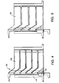
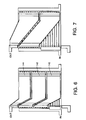
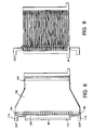
- Figs. 2 through 10 are plan views of various turns arrangements.
- Fig. 11 is a chart of turns arrangements.
- Fig. 12 is a perspective view showing a bridge.
- Figs. 13 and 14 are cross-sectional views illustrating taps.
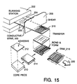
- Fig. 15 is a schematic perspective view of a method of fabrication.
- Figs. 16 and 17 are cross-sectional views illustrating methods of incorporating flux-shunts for adjusting the values of leakage inductances.
- a transformer 10 formed on a printed circuit board 12, includes a primary winding 14 and a secondary winding 16 which partially lie within a passageway 18 formed between two magnetic core pieces 20, 22.
- Secondary winding 16 includes a row of flat conductors 24, 26, 28 (some of the conductors in the row are not shown) which are electrically connected to a corresponding row of conductive runs 30, 32, 34 formed on the surface of the printed circuit board as part of the board fabrication process.
- the electrical connections are made at connection pads, e.g., 35, 37, which are physically no different (except in shape) from the runs.
- the conductors are generally rectangular in cross-section and have a relatively high aspect ratio, at least 2.
- the primary winding like the secondary winding, includes a row of flat conductors 36, 38, 40 (some not shown) connected to a corresponding row of conductive runs which are formed on the underside of printed circuit board 12 (and thus not shown in Fig. 1).
- the connections between the conductors and conductive runs of the primary winding are made via connection pads, e.g., 42, 44, 46, and plated-through holes, e.g., 48, 50, 52.
- Circuit connections to the primary and secondary windings are made via conductive runs 60, 62, 64, and 66.
- a dielectric layer 70 is interposed to insulate the conductors of the primary winding from the conductors of the secondary winding.
- Each core piece 20, 22 is, e.g., U-shaped and the legs of the Us meet to form a magnetic circuit with no gap or with a preselected gap 72 (as discussed in more detail below).
- a simpler electromagnetic component e.g., an inductor
- an inductor can be formed using a similar configuration by eliminating the conductors 36, 38, 40, and the related conductive runs and connection pads from the printed circuit board, thus leaving a single winding with two magnetic core pieces. By also eliminating the magnetic core pieces, a simple coil can be formed.
- each winding comprises conductive runs on the printed circuit board (substrate) and conductors connected to the conductive runs.
- the number of turns in each winding is determined by the number of conductors used, rather than by the number of conductive runs on the printed circuit board, because any conductor may be connected either to one or to more than one conductive run. This is especially significant because a single pattern of conductive runs formed on a printed circuit board can be used as the basis for fabricating windings of a variety of numbers of turns. (And, in the case of a transformer, the turns ratio of the primary to secondary windings also can be varied by controlling the numbers of turns in each winding.)
- a fixed pattern of conductive runs 100 positioned on a printed circuit board for use in forming windings having selected numbers of turns could include a row of twenty parallel straight conductive runs 102.
- the ends of the conductive runs terminate in connection pads 104, 106.
- Each run could be, for example, 0.03 inches wide and 1.1 inches long with a separation of 0.01 inches between adjacent runs.
- Additional conductive runs 108, 110, 112, and 114 are provided for making connections as explained below.
- a 10-turn winding can be formed on the pattern of Fig. 2 by connecting a row of ten conductors 116 to the row of 20 conductive runs as follows. One end 118 of each conductor is connected to the connection pads of a first pair of adjacent conductive runs (not seen in Fig. 3). Except for the uppermost conductor in Fig. 3, the left end 122 of each conductor is connected to the connection pads 122, 124 of another pair of adjacent conductive runs. Each conductor has a jog 120 configured so that the opposite ends of the conductor are respectively connected to two different pairs of conductive runs. In this way a continuous winding is created.
- conductive run 114 has its left end connected to conductive run 114 to carry current out of the winding.
- a bridge 126 connects conductive run 112 (which provides a path for current into the winding) to the lowermost pair of conductive runs 102 in Fig. 3. The resulting winding has 10 turns.
- the same pattern of conductive runs can be used to form a 5 turn winding by providing five conductors 130, each having a width approximately equal to the width of the space occupied by four conductive runs.
- the jog 132 in each conductor is configured so that the set of four conductive runs connected to one end of the conductor are different from the set of four conductive runs connected to the other end of the conductor.
- a bridge 134 connects the lowermost four conductive runs to the conductive run 112.
- a 4 turn winding has four conductors 136 each wide enough to span five conductive runs.
- a 3 turn winding has two conductors 140, 142 each spanning seven conductive runs and one conductor 144 spanning six conductive runs.
- a 2 turn winding uses two conductors each spanning ten conductive runs.
- twenty conductors each span a single conductive run to form a 20 turn winding.
- a single conductor 150 spans all twenty conductive runs.
- One end 152 of the conductor is connected to the connection pads of all twenty conductive runs.
- the other end broadens to form two legs 154 connected respectively to conductive runs 114, and 110, which carry current out of the winding.
- a bridge 158 connects all of the connection pads on the left ends of the conductive runs to conductive run 112 to provide a path for current into the winding.
- a tap conductive run 108 can be connected by a bridge 160 to one of the conductors as shown to provide a tap connection to the winding.
- any number of desired turns from 1 to 20 can be made by an appropriate choice of the number and widths of conductors to be connected to the fixed pattern of conductive runs.
- the chart of Fig. 11 assumes that all of the conductive runs are used.
- the conductors are all of equal widths for 1, 2, 4, 5, 10, and 20 turn windings; for other windings, conductors of two widths are used.
- an 8 turn winding could also be formed using four "4-wide" conductors and four "1-wide" conductors. Windings could also be formed by using fewer than the total number of conductive runs.
- a bridge 190 allows for large area winding terminations which are useful for windings with small numbers of turns.
- the bridges are also useful in windings that use fewer than all of the conductive runs.
- a 17 turn winding can be implemented by using 17 "1-wide" conductors, 17 conductive runs, and a bridge connection from the 17th run to the input or output conductive run. Three of the conductive runs would then remain unused.
- taps can be formed by increasing the length of the end 192 of a conductor so that it connects to another conductive run 194 on the substrate.
- a tap in the case of a transformer, can be formed on the upper winding by similarly extending the end 196 of a conductor to reach a separate conductive run 198 on the substrate.
- two or more independent windings can be formed from a single row of conductors.
- twenty equal width conductors combined with a pattern of twenty conductive runs could be used to form two independent ten-turn windings; a seventeen-turn and a three-turn winding; or three six-turn windings (in this case, two of the conductors would not be used).
- the only restriction is that the sum of the turns formed by the various windings cannot be greater than the number of conductive runs to which the row of conductors is attached.
- each winding can be formed with any number of turns selected from among the set of possible numbers of turns.
- the number and configuration of the required conductors are determined from the selected number of turns and from the pattern of conductive runs and pads on the printed circuit board, as indicated above.
- the conductors are created in "real time", i.e., at the time they are required for use in the particular winding to be installed on a printed circuit board on an assembly line.
- the conductors are formed on a continuous stock of flat conductive (e.g., copper-or brass) strip 200, by laser cutting the strip in a blanking station 202 to create a pattern of the required conductors 204 together with supporting areas 206 to hold the conductors in proper orientation during the initial stages of fabrication.
- the laser cutter may be controlled by a computer to permit lot of one fabrication of patterns.
- the piece is severed from the strip of stock by a shear 208.
- a core piece 210 is coated with adhesive 212, and the coated piece 214 is delivered to a position in which the patterned piece 216 can be bent over coated piece 214 to its final form.
- the supporting areas 206 are then trimmed 218 and the assembled piece is delivered 220 to the location where it can be mounted on the pattern of conductive runs on the printed circuit board.
- the dielectric layer is placed over the patterned piece, the patterned piece for the primary winding (formed in the same way as the secondary patterned piece) is placed over the dielectric layer, and the top magnetic core piece is overlaid on and attached to the dielectric with the legs of the Us of the two pieces aligned.
- the resulting subassembly is further processed by severing the supporting areas from the conductors of the primary winding.
- the finished subassembly is then laid over the conductive run pattern on the printed circuit board, with the ends of the conductors of the two windings overlaid on the connection pads of the corresponding conductive runs. (Earlier in the fabrication process, "dots" of solder paste were placed on the connection pads and the solder dots now rest between the flat surfaces of the conductors and the conductive runs).
- Bridge conductors could also be formed in the blanking station 202, or, alternatively, they might be separately cut to length from strip stock at another station (not shown) for placement onto the pattern of conductive runs at an appropriate stage in the assembly process.
- the solder is reflowed, thus forming low resistance electrical connections between each conductor and the corresponding conductive run (or runs).
- the electrical connections exhibit low resistance because they are formed at relatively broad connection regions and thus have a relatively large cross-sectional area, and because the distance between the mating surfaces of the conductors and the connection pads are small due to the precision with which the parts can be manufactured.
- the windings have relatively low total resistance and are thus suitable both for signal applications and power applications.
- the fabrication sequence for other kinds of electromagnetic components could be similar, with differences in, for example, the number of windings that are formed and the number and configurations of the core pieces.
- the windings of the electromagnetic component will exhibit values of self-inductance and leakage inductance which are dependent on the physical size and geometry of the magnetic core pieces and the windings; the spatial relationship between the magnetic core pieces and the windings; the number of turns on the windings; and the magnetic characteristics of the core pieces.
- the magnetic core pieces may be configured to provide a gap 72 (Fig. 1) in the magnetic circuit.
- One simple way of providing a carefully controlled gap is to insert a non-magnetic shim of appropriate thickness between the two core pieces.
- Leakage inductance which accounts for flux generated in a winding which does not couple into other windings (and which may be useful, for example, in power converter circuits of the kind shown in Vinciarelli, United States Patent 4,415,959, incorporated by reference), can be augmented through use of flux-shunts which can be sandwiched between windings and core pieces (one example of which is shown at 250 in Fig. 16), or which can be placed in proximity to the conductors after they exit from the core (one example of which is shown at 252 in Fig. 17).
- a discrete electromagnetic component could be formed using a substrate and conductors and without other circuit elements mounted on the substrate.
- the insulating layer could be wound around one or more of the winding patterns prior to the winding pattern being placed onto the component; the supporting areas for one or more of the conductive strips could be severed just after the strip was placed upon the component; different parts could be attached to other parts during the fabrication process using adhesive to ensure correct alignment.
- the sheet metal work piece could be, for example, die cut instead of laser cut.
- the conductors could be- individually formed from strip stock, or formed on printed circuit boards with appropriate terminations.
- Conductive epoxy, or another conductive joint compound, might be used instead of solder, or another method of forming the conductive joints might be used, such as welding.
- the magnetic core pieces need not be U-shaped.
Landscapes
- Engineering & Computer Science (AREA)
- Power Engineering (AREA)
- Manufacturing & Machinery (AREA)
- Microelectronics & Electronic Packaging (AREA)
- Coils Of Transformers For General Uses (AREA)
- Coils Or Transformers For Communication (AREA)
Applications Claiming Priority (2)
| Application Number | Priority Date | Filing Date | Title |
|---|---|---|---|
| US59889690A | 1990-10-16 | 1990-10-16 | |
| US598896 | 1990-10-16 |
Publications (2)
| Publication Number | Publication Date |
|---|---|
| EP0481755A2 true EP0481755A2 (de) | 1992-04-22 |
| EP0481755A3 EP0481755A3 (en) | 1992-12-09 |
Family
ID=24397375
Family Applications (1)
| Application Number | Title | Priority Date | Filing Date |
|---|---|---|---|
| EP19910309527 Withdrawn EP0481755A3 (en) | 1990-10-16 | 1991-10-16 | Electromagnetic windy structures, and methods for forming electromagnetic winding structures |
Country Status (2)
| Country | Link |
|---|---|
| EP (1) | EP0481755A3 (de) |
| JP (1) | JPH0653055A (de) |
Cited By (6)
| Publication number | Priority date | Publication date | Assignee | Title |
|---|---|---|---|---|
| EP0632472A1 (de) * | 1993-06-01 | 1995-01-04 | Eaton Corporation | Stromwandler mit einem laminierten Ringkern und mit einem Leiterrahmen |
| FR2721431A1 (fr) * | 1994-06-20 | 1995-12-22 | Ies | Procédé pour réaliser des composants magnétiques à bobinages simplifiés, et composants ainsi réalisés. |
| US6188305B1 (en) | 1995-12-08 | 2001-02-13 | International Business Machines Corporation | Transformer formed in conjunction with printed circuit board |
| WO2003005579A1 (en) * | 2001-07-04 | 2003-01-16 | Koninklijke Philips Electronics N.V. | Electronic inductive and capacitive component |
| US6664881B1 (en) * | 1999-11-30 | 2003-12-16 | Ameritherm, Inc. | Efficient, low leakage inductance, multi-tap, RF transformer and method of making same |
| WO2007072375A3 (en) * | 2005-12-22 | 2007-11-01 | Koninkl Philips Electronics Nv | Method for manufacturing a microelectronic device, wherein at least one electrically conductive winding is arranged around a ferrite core element |
Families Citing this family (2)
| Publication number | Priority date | Publication date | Assignee | Title |
|---|---|---|---|---|
| JP4547889B2 (ja) * | 2003-10-21 | 2010-09-22 | Tdk株式会社 | 磁気結合素子 |
| JP7816933B2 (ja) * | 2020-08-17 | 2026-02-18 | Tdk株式会社 | コイル装置 |
Family Cites Families (3)
| Publication number | Priority date | Publication date | Assignee | Title |
|---|---|---|---|---|
| US3614554A (en) * | 1968-10-24 | 1971-10-19 | Texas Instruments Inc | Miniaturized thin film inductors for use in integrated circuits |
| DE3044332A1 (de) * | 1980-04-25 | 1982-06-16 | Siemens AG, 1000 Berlin und 8000 München | Hybridschaltung |
| US4455545A (en) * | 1982-11-05 | 1984-06-19 | Sperry Corporation | High frequency output inductor for inverter power supply |
-
1991
- 1991-10-16 JP JP3332999A patent/JPH0653055A/ja active Pending
- 1991-10-16 EP EP19910309527 patent/EP0481755A3/en not_active Withdrawn
Cited By (6)
| Publication number | Priority date | Publication date | Assignee | Title |
|---|---|---|---|---|
| EP0632472A1 (de) * | 1993-06-01 | 1995-01-04 | Eaton Corporation | Stromwandler mit einem laminierten Ringkern und mit einem Leiterrahmen |
| FR2721431A1 (fr) * | 1994-06-20 | 1995-12-22 | Ies | Procédé pour réaliser des composants magnétiques à bobinages simplifiés, et composants ainsi réalisés. |
| US6188305B1 (en) | 1995-12-08 | 2001-02-13 | International Business Machines Corporation | Transformer formed in conjunction with printed circuit board |
| US6664881B1 (en) * | 1999-11-30 | 2003-12-16 | Ameritherm, Inc. | Efficient, low leakage inductance, multi-tap, RF transformer and method of making same |
| WO2003005579A1 (en) * | 2001-07-04 | 2003-01-16 | Koninklijke Philips Electronics N.V. | Electronic inductive and capacitive component |
| WO2007072375A3 (en) * | 2005-12-22 | 2007-11-01 | Koninkl Philips Electronics Nv | Method for manufacturing a microelectronic device, wherein at least one electrically conductive winding is arranged around a ferrite core element |
Also Published As
| Publication number | Publication date |
|---|---|
| JPH0653055A (ja) | 1994-02-25 |
| EP0481755A3 (en) | 1992-12-09 |
Similar Documents
| Publication | Publication Date | Title |
|---|---|---|
| KR100373410B1 (ko) | 다층 프린터 코일기판의 제조방법과 프린터 코일부품 및 프린터 코일 기판 | |
| EP0953994B1 (de) | Mehrschichtige Induktivität und Verfahren zu ihrer Herstellung | |
| US5801611A (en) | Inductive device | |
| US6000128A (en) | Process of producing a multi-layered printed-coil substrate | |
| US7477124B2 (en) | Method of making slotted core inductors and transformers | |
| JPH0869935A (ja) | 多層プリントコイル基板の作製方法並びにプリントコイル基板及び多層プリントコイル基板 | |
| US20130113591A1 (en) | Magnetic electrical device | |
| US20040130428A1 (en) | Surface mount magnetic core winding structure | |
| US20020149461A1 (en) | Apparatus and method for PCB winding planar magnetic devices | |
| EP0756298A2 (de) | Elektronische induktive Vorrichtung und Herstellungsverfahren | |
| US20040178489A1 (en) | Multilayer circuit and method of manufacturing | |
| US6675462B1 (en) | Method of manufacturing a multi-laminated inductor | |
| WO2006026674A2 (en) | Precision inductive devices and methods | |
| US6844804B2 (en) | Method of manufacturing discrete electronic components | |
| EP0481755A2 (de) | Elektromagnetische Windungsanordnungen, und Verfahren zur Herstellung von elektromagnetischen Windungsanordnungen | |
| JP2770750B2 (ja) | インダクタンス素子 | |
| EP1332503B1 (de) | Induktive bauelemente | |
| US5694104A (en) | Low profile high power surface mount transformer | |
| JP3598405B2 (ja) | プリントコイル部品及びプリントコイル基板 | |
| JP2510787B2 (ja) | 端子付コイルボビン | |
| US4320373A (en) | Power transformer with high coupling coefficient | |
| JPH08273944A (ja) | 平面型トランス | |
| GB2301489A (en) | A power output module for a power supply unit | |
| JPH08138939A (ja) | 積層型コイル | |
| HK1021851B (en) | Multi-laminated inductor and manufacturing method thereof |
Legal Events
| Date | Code | Title | Description |
|---|---|---|---|
| PUAI | Public reference made under article 153(3) epc to a published international application that has entered the european phase |
Free format text: ORIGINAL CODE: 0009012 |
|
| AK | Designated contracting states |
Kind code of ref document: A2 Designated state(s): AT BE CH DE DK ES FR GB GR IT LI LU NL SE |
|
| PUAL | Search report despatched |
Free format text: ORIGINAL CODE: 0009013 |
|
| AK | Designated contracting states |
Kind code of ref document: A3 Designated state(s): AT BE CH DE DK ES FR GB GR IT LI LU NL SE |
|
| STAA | Information on the status of an ep patent application or granted ep patent |
Free format text: STATUS: THE APPLICATION IS DEEMED TO BE WITHDRAWN |
|
| 18D | Application deemed to be withdrawn |
Effective date: 19930610 |