EP0482536A2 - Convertisseur de tension à sortie commutable - Google Patents
Convertisseur de tension à sortie commutable Download PDFInfo
- Publication number
- EP0482536A2 EP0482536A2 EP91117862A EP91117862A EP0482536A2 EP 0482536 A2 EP0482536 A2 EP 0482536A2 EP 91117862 A EP91117862 A EP 91117862A EP 91117862 A EP91117862 A EP 91117862A EP 0482536 A2 EP0482536 A2 EP 0482536A2
- Authority
- EP
- European Patent Office
- Prior art keywords
- voltage
- output
- digital logic
- input
- reference voltage
- Prior art date
- Legal status (The legal status is an assumption and is not a legal conclusion. Google has not performed a legal analysis and makes no representation as to the accuracy of the status listed.)
- Withdrawn
Links
- 230000001105 regulatory effect Effects 0.000 claims abstract description 15
- 239000003990 capacitor Substances 0.000 claims description 10
- 230000003213 activating effect Effects 0.000 claims 2
- 230000005669 field effect Effects 0.000 description 2
- 240000004053 Rorippa indica Species 0.000 description 1
- 238000006243 chemical reaction Methods 0.000 description 1
- 238000004904 shortening Methods 0.000 description 1
- 230000000087 stabilizing effect Effects 0.000 description 1
Images

Classifications
-
- H—ELECTRICITY
- H02—GENERATION; CONVERSION OR DISTRIBUTION OF ELECTRIC POWER
- H02M—APPARATUS FOR CONVERSION BETWEEN AC AND AC, BETWEEN AC AND DC, OR BETWEEN DC AND DC, AND FOR USE WITH MAINS OR SIMILAR POWER SUPPLY SYSTEMS; CONVERSION OF DC OR AC INPUT POWER INTO SURGE OUTPUT POWER; CONTROL OR REGULATION THEREOF
- H02M3/00—Conversion of DC power input into DC power output
- H02M3/02—Conversion of DC power input into DC power output without intermediate conversion into AC
- H02M3/04—Conversion of DC power input into DC power output without intermediate conversion into AC by static converters
- H02M3/10—Conversion of DC power input into DC power output without intermediate conversion into AC by static converters using discharge tubes with control electrode or semiconductor devices with control electrode
- H02M3/145—Conversion of DC power input into DC power output without intermediate conversion into AC by static converters using discharge tubes with control electrode or semiconductor devices with control electrode using devices of a triode or transistor type requiring continuous application of a control signal
- H02M3/155—Conversion of DC power input into DC power output without intermediate conversion into AC by static converters using discharge tubes with control electrode or semiconductor devices with control electrode using devices of a triode or transistor type requiring continuous application of a control signal using semiconductor devices only
- H02M3/156—Conversion of DC power input into DC power output without intermediate conversion into AC by static converters using discharge tubes with control electrode or semiconductor devices with control electrode using devices of a triode or transistor type requiring continuous application of a control signal using semiconductor devices only with automatic control of output voltage or current, e.g. switching regulators
-
- G—PHYSICS
- G05—CONTROLLING; REGULATING
- G05F—SYSTEMS FOR REGULATING ELECTRIC OR MAGNETIC VARIABLES
- G05F1/00—Automatic systems in which deviations of an electric quantity from one or more predetermined values are detected at the output of the system and fed back to a device within the system to restore the detected quantity to its predetermined value or values, i.e. retroactive systems
- G05F1/10—Regulating voltage or current
- G05F1/46—Regulating voltage or current wherein the variable actually regulated by the final control device is DC
- G05F1/56—Regulating voltage or current wherein the variable actually regulated by the final control device is DC using semiconductor devices in series with the load as final control devices
- G05F1/563—Regulating voltage or current wherein the variable actually regulated by the final control device is DC using semiconductor devices in series with the load as final control devices including two stages of regulation at least one of which is output level responsive, e.g. coarse and fine regulation
Definitions
- the present invention relates to a multiple output power source, and more particularly to a switchable output voltage converter providing selectable DC output voltage levels.
- power sources capable of providing a plurality of DC output voltage levels.
- a single power source is used to provide these outputs.
- these power sources have a number of output terminals supplying the required voltage levels simultaneously. If, however, it is not necessary to output the required voltage levels simultaneously, a single output terminal is sufficient. Means must be provided, therefore, to select and vary the voltage level outputted at this terminal.
- a power supply for providing a selectable predetermined regulated output voltage is disclosed.
- a switching regulator circuit converts an input voltage to a DC output voltage and a control circuit, which senses the output voltage, controls the conversion of the switching regulator circuit.
- An amplifier having selectable gain values is interposed between the control circuit and the output terminal of the power supply. In this manner, a predetermined portion of the output voltage is used as feedback to the control circuit, permitting selective determination of the output voltage without altering the switching regulator circuit or the control circuit.
- Genuit can supply a plurality of output voltage levels without necessitating changes to either the switching regulator circuit or the control circuit, the gain of the feedback amplifier must be altered.
- the feedback resistors are selectably connected across the amplifier by means of switches to accomplish the required gain change.
- the amplifier gain may be altered by installing jumpers across various points in the feedback resistor network. In either of these instances, the required amplifier gain change is accomplished through manual means of installing the jumpers or changing the switch positions.
- U.S. Patent 4,677,534 to Okochi discloses a multiple output power source capable of generating both AC and DC output voltages.
- a pulse width modulator compares a triangle wave from an oscillator with an error voltage from a differential amplifier.
- the pulse width modulator output drives a switching transistor in a manner which controls the DC voltage output level.
- no means are provided for selectively determining a plurality of DC output voltage levels.
- U.S. Patens 4,460,949 to Steigerwald discloses a DC-DC converter driven by an inverter providing square waves of current to a parallel resonant circuit. By varying the frequency at which the inverter switches turn ON and OFF, the output of the parallel resonant circuit is altered. This output is then rectified to provide the DC output voltage. Steigerwald, however, provides no means to selectively choose one of a predetermined number of DC output voltage levels.
- a switchable output voltage converter which converts an unregulated voltage input to a regulated DC output.
- the regulated DC output level is selectable by means of at least one digital logic input to the converter. Altering the status of a digital logic input permits real time control of the voltage converter output.
- the regulated DC output voltage level depends on the value of a reference voltage fed into the converter, in addition to the status of the digital logic input.
- An error amplifier compares a portion of the present output voltage with a portion of the reference voltage and outputs an error voltage.
- a pulse width modulator compares this error voltage to a sawtooth waveform and outputs a pulse waveform which varies the duty cycle of a switching transistor to maintain the output voltage at its desired level.
- the output voltage of the converter circuit is linearly related to the portion of the reference voltage fed into the error amplifier.
- This portion of the reference voltage can be altered to obtain a particular output voltage by the use of an incrementally variable resistance network.
- the resistance network comprises a digital logic input, a resistor, a field effect transistor (FET) switch, and an inverter.
- FET field effect transistor
- the FET is turned ON or OFF by the digital logic input fed into the inverter.
- the portion of the reference voltage fed into the error amplifier is altered. Because the output voltage is linearly related to this portion of the reference voltage, one of two output voltages can be selected by changing the state of the digital logic input.
- More than two output voltage levels are selectable by adding a second resistor, FET switch, inverter and digital logic input. Such an arrangement would provide for four possible logic input combinations and, hence, four possible values for the proportion of reference voltage fed back into the error amplifier. In this manner, the status of the two digital logic inputs will determine which one of four output voltage levels is obtained.
- the voltage converter circuit is expandable in a similar manner by adding additional resistors, FET
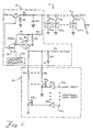
- FIG. 1 is a schematic illustration of a switchable output voltage converter circuit 10.
- the converter circuit 10 comprises a control circuit 12 and an output selector circuit 14.
- the control circuit 12 provides an output voltage (shown as V OUT ) at an output terminal 16 of the control circuit which is linearly related to a portion of a reference voltage (shown as V REF ) fed into an error amplifier 18 of the control circuit.
- V REF a reference voltage
- This portion of the reference voltage can be altered to obtain a particular output voltage by enabling the output selection circuit 14.
- By selectably alternating a digital logic input 20 between LOW and HIGH the portion of the reference voltage fed into the error amplifier 18 is altered. Because the output voltage is linearly related to this portion of the reference voltage, one of two specific output voltages can be selected by changing the state of the digital logic input 20.
- V IN the same input voltage
- V IN the same input voltage
- switches 24a and 24b the same input voltage
- the control circuit 12 converts the unregulated input voltage to a regulated output voltage and maintains the voltage at a desired level.
- the unregulated input voltage is in the form of a rectified AC voltage waveform and is of greater amplitude than either of the two selectable output voltages.
- the rectified voltage waveform is smoothed by an inductor 26 and a capacitor 28 to provide the regulated DC output voltage in a well known manner.
- the error amplifier 18 of the control circuit 12 compares portions of the output voltage and reference voltage and outputs an error voltage.
- Resistor R1 acts as a feedback resistor for the error amplifier.
- Resistor R1 is typically in the range of 100K ohms and provides a means of stabilizing the operation of the error amplifier 18.
- a fractional portion of the regulated output voltage is fed into a first input 30 of the error amplifier 18 through a first pair of input resistors R2 and R3, each having a resistance less than 10K ohms. This fractional portion of the output voltage equals R3/(R2 + R3) of the output voltage, because the resistance value of R1 is so much greater than that of R3.
- a fractional portion of the reference voltage is similarly fed into a second input 32 of the error amplifier 18 through a second pair of input resistors R4 and R5, each having a resistance of less than 10K ohms. This fractional portion equals R5/(R4 + R5) of the reference voltage.
- the error amplifier compares these two voltages and outputs an error voltage (shown as V ERR ) representing the difference between these two voltages.
- the error voltage and a sawtooth waveform outputted by a sawtooth oscillator 34 are compared by a pulse width modulator 36.
- the pulse width modulator 36 converts the sawtooth waveform to pulses of the same frequency as the sawtooth waveform.
- the pulse width is varied in response to the error voltage and is supplied to the base of a switching transistor 38.
- the pulse width is shortened if the error amplifier indicates that the output voltage is too high, and is lengthened if a low voltage is indicated.
- the pulse width modulator thus controls the duty cycle of transistor 38 which determines the average value of unregulated voltage fed into the inductor-capacitor filter.
- a diode 39 allows stored current in the inductor 26 to flow to ground at any time transistor 38 is turned OFF.
- the diode 39 does not conduct during times at which the transistor is switched ON. In this manner, the control circuit 10 is able to maintain the output voltage at its desire, level.
- the output voltage is represented by the following equation:
- the output selection circuit 14 provides means to control the output so that one of two output voltages can be supplied to either of two electrical loads 22a or 22b.
- the output selection circuit 14 comprises a digital logic input 20, an inverter 40, a field effect transistor (FET) 42, and a resistor R6.
- the status of the digital logic input 24 determines whether the output selection circuit 14 is activated or deactivated. If the status of the digital logic input is HIGH, the inverter 40 inverts the HIGH to LOW and the FET 42 remains OFF. Resistor R6 does not affect the operation of the control circuit 12 because it draws no current, and the output of the inverter circuit 10 is represented by equation 1 above.
- the output selection circuit 14 is activated by a LOW digital logic input 20.
- the LOW input is inverted to a HIGH by the inverter 40, thereby turning FET 42 ON.
- Resistor R6 begins to draw current, and the voltage level at the second input 32 to the error amplifier 16 is lowered.
- the error amplifier 18 responds by outputting an error voltage representing the voltage differential present between the first input 30 and the second input 32.
- the pulse width modulator in turn responds to this error voltage by shortening the pulse width of its output to reduce the duty cycle of transistor 38.
- the average value of unregulated voltage fed into the inductor-capacitor filter is thus lowered, thereby reducing the level of the output voltage.
- the output voltage of the converter circuit 10 when the digital logic input is LOW is represented by the following equation:
- a LOW logic input to the output selection circuit 14 effectively reduces the portion of the reference voltage fed into the second input 32 to the error amplifier 18. Because the output voltage of the converter circuit 10 is linearly related to this portion of the reference voltage, as shown by equations 1 and 2, one of the two output voltages represented by these equations is selectable by changing the state of the digital logic input 20. In this manner, selective determination of the converter circuit output is provided by the digital logic input without necessitating changes to component values in either the control circuit 12 or the output selection circuit 14. In addition, means are provided to operate switches 24a and 24b simultaneously with changes in the digital logic input to select whether load 22a or 22b is to be connected to the output terminal 16.
- the output selection circuit 14 is expandable to enable the converter circuit 10 to output one of more than two selectable output voltages.
- Figure 2 shows an expanded selectable output circuit 14. Resistors R6 through Rn are selectively brought into the circuit separately or in any parallel combination by means of the digital logic inputs 20a through 20n, inverters 40a through 40n, and FETs 42a through 42n. A different portion of the reference voltage is fed into the second input 32 of the error amplifier 18 for each combination of resistors brought into the circuit.
- the converter circuit 10 is capable of providing a specific voltage output. In general, the converter is capable of providing any one of 2 n different output voltages, where n equals the number of digital logic inputs.
- the circuit permits real time control of the regulated output voltage level which depends on the values chosen for the inductor 26 and the capacitor 28. Typically, component values will be near 10K ⁇ F for capacitor 28 and 200 ⁇ H for inductor 26, which permit the control circuit to respond to load changes within 100 milliseconds. If the load connected to the output terminal 16 of the voltage converter increases, the output voltage level will be reduced at the output terminal 16. The time it takes for the control circuit to increase the output voltage to the desired level depends on how quickly the inductor-capacitor filter can be charged. Should the load decrease, the output voltage at terminal 16 will increase. The rate at which capacitor 28 discharges will determine the time it takes for the control circuit to decrease the output voltage to the desired level.
- the capacitor 28 discharges through the load connected to the output terminal 16 or an optimal discharge resistor 44.
- the discharge resistor 44 is permanently paralleled across the output terminal and ground.
- the discharge resistor is selectively engaged by well known means during the time it takes for the control circuit to decrease the output voltage to the desired level.
- a switchable output voltage converter having selectable output circuit means which may provide one of two predetermined output voltages. Further, the selectable output circuit means are expandable to enable the converter to provide any one of a plurality of predetermined output voltages.
Landscapes
- Engineering & Computer Science (AREA)
- Power Engineering (AREA)
- Physics & Mathematics (AREA)
- Electromagnetism (AREA)
- General Physics & Mathematics (AREA)
- Radar, Positioning & Navigation (AREA)
- Automation & Control Theory (AREA)
- Dc-Dc Converters (AREA)
Applications Claiming Priority (2)
| Application Number | Priority Date | Filing Date | Title |
|---|---|---|---|
| US602023 | 1984-04-24 | ||
| US07/602,023 US5084666A (en) | 1990-10-23 | 1990-10-23 | Switchable output voltage converter |
Publications (2)
| Publication Number | Publication Date |
|---|---|
| EP0482536A2 true EP0482536A2 (fr) | 1992-04-29 |
| EP0482536A3 EP0482536A3 (en) | 1992-08-12 |
Family
ID=24409662
Family Applications (1)
| Application Number | Title | Priority Date | Filing Date |
|---|---|---|---|
| EP19910117862 Withdrawn EP0482536A3 (en) | 1990-10-23 | 1991-10-19 | Switchable output voltage converter |
Country Status (2)
| Country | Link |
|---|---|
| US (1) | US5084666A (fr) |
| EP (1) | EP0482536A3 (fr) |
Cited By (1)
| Publication number | Priority date | Publication date | Assignee | Title |
|---|---|---|---|---|
| EP0592804A1 (fr) * | 1992-10-13 | 1994-04-20 | Robert Bosch Gmbh | Dispositif pour la commande de plusieurs actionneurs à courant stabilisé au moyen d'un ordinateur de commande |
Families Citing this family (25)
| Publication number | Priority date | Publication date | Assignee | Title |
|---|---|---|---|---|
| US5289361A (en) * | 1991-01-16 | 1994-02-22 | Vlt Corporation | Adaptive boost switching preregulator and method |
| KR920017329A (ko) * | 1991-02-22 | 1992-09-26 | 원본미기재 | 적응전압 조정기 |
| US5245526A (en) * | 1992-02-07 | 1993-09-14 | Power Integrations, Inc. | Below ground current sensing with current input to control threshold |
| US5319303A (en) * | 1992-02-12 | 1994-06-07 | Sony/Tektronix Corporation | Current source circuit |
| US5399908A (en) * | 1992-06-26 | 1995-03-21 | Kollmorgen Corporation | Apparatus and method for forced sharing of parallel MOSFET switching losses |
| US5260643A (en) * | 1992-07-16 | 1993-11-09 | National Semiconductor Corporation | Programmable reference voltage generator |
| CA2084833A1 (fr) * | 1992-12-08 | 1994-06-09 | I-Chang Chang | Alimentation en courant continu a tension variable, rechargeable et portative |
| US5532576A (en) * | 1994-04-11 | 1996-07-02 | Rockwell International Corporation | Efficient, well regulated, DC-DC power supply up-converter for CMOS integrated circuits |
| US7145787B2 (en) * | 1994-04-26 | 2006-12-05 | Comarco Wireless Technologies, Inc. | Programmable power supply |
| US6693413B1 (en) | 1994-04-26 | 2004-02-17 | Comarco Wireless Technologies, Inc. | Programmable power supply |
| US6831848B2 (en) | 1994-04-26 | 2004-12-14 | Comarco Wireless Technologies, Inc. | Programmable power supply to simultaneously power a plurality of electronic devices |
| EP0681362B1 (fr) * | 1994-05-06 | 1998-10-28 | STMicroelectronics S.r.l. | Commande numérique en mode de courant pour modulation de largeur d'impulsions |
| US5781000A (en) * | 1995-06-16 | 1998-07-14 | Fujitsu Limited | Power control unit loading test method |
| US5790392A (en) * | 1996-01-23 | 1998-08-04 | Micro Motion, Inc. | Intelligent power supply with staged loading capability |
| US5877611A (en) * | 1996-10-09 | 1999-03-02 | Lucent Technologies Inc. | Simple and efficient switching regulator for fast transient loads such as microprocessors |
| US6104414A (en) * | 1997-03-12 | 2000-08-15 | Cybex Computer Products Corporation | Video distribution hub |
| JP2002042468A (ja) * | 2000-07-21 | 2002-02-08 | Oki Electric Ind Co Ltd | 半導体集積回路 |
| US6522110B1 (en) * | 2001-10-23 | 2003-02-18 | Texas Instruments Incorporated | Multiple output switching regulator |
| US9153960B2 (en) | 2004-01-15 | 2015-10-06 | Comarco Wireless Technologies, Inc. | Power supply equipment utilizing interchangeable tips to provide power and a data signal to electronic devices |
| JP2010074891A (ja) * | 2008-09-16 | 2010-04-02 | Sanyo Electric Co Ltd | 半導体回路 |
| JP2010198570A (ja) * | 2009-02-27 | 2010-09-09 | Panasonic Corp | 電圧供給回路 |
| US8213204B2 (en) * | 2009-04-01 | 2012-07-03 | Comarco Wireless Technologies, Inc. | Modular power adapter |
| US8354760B2 (en) * | 2009-10-28 | 2013-01-15 | Comarco Wireless Technologies, Inc. | Power supply equipment to simultaneously power multiple electronic device |
| US9083237B2 (en) | 2010-07-13 | 2015-07-14 | O2Micro, Inc. | Circuits and methods for controlling a DC/DC converter |
| CN115296527A (zh) * | 2022-07-22 | 2022-11-04 | 北京时代民芯科技有限公司 | 一种基于dc-dc转换器的输出版本可配置电路 |
Family Cites Families (22)
| Publication number | Priority date | Publication date | Assignee | Title |
|---|---|---|---|---|
| US3755686A (en) * | 1972-05-31 | 1973-08-28 | Nasa | Powerplexer |
| JPS5552117A (en) * | 1978-10-11 | 1980-04-16 | Fanuc Ltd | Dc stabilized power supply unit |
| US4594501A (en) * | 1980-10-09 | 1986-06-10 | Texas Instruments Incorporated | Pulse width modulation of printhead voltage |
| JPS5783832A (en) * | 1980-11-12 | 1982-05-25 | Sanyo Kiko Kk | Constant voltage power source of digital control |
| JPS57141727A (en) * | 1981-02-27 | 1982-09-02 | Ricoh Co Ltd | Multistage output power supply circuit |
| US4388587A (en) * | 1981-12-17 | 1983-06-14 | Motorola, Inc. | Fixed frequency voltage regulator |
| JPS58219622A (ja) * | 1982-06-15 | 1983-12-21 | Fuji Xerox Co Ltd | 基準電圧発生回路 |
| US4460949A (en) * | 1982-09-30 | 1984-07-17 | General Electric Company | High frequency parallel resonant dc-dc converter |
| JPS6020394A (ja) * | 1983-07-14 | 1985-02-01 | Ricoh Co Ltd | 電源切換回路 |
| JPS60121931A (ja) * | 1983-12-06 | 1985-06-29 | 富士写真フイルム株式会社 | 直流電源装置 |
| US4569009A (en) * | 1984-03-05 | 1986-02-04 | Honeywell Information Systems Inc. | Switching regulator having a selectable gain amplifier for providing a selectively alterable output voltage |
| JPS60220412A (ja) * | 1984-04-17 | 1985-11-05 | Fujitsu Ltd | 出力電圧プログラム回路 |
| DE3588108T2 (de) * | 1984-12-28 | 1996-11-07 | Toshiba Kawasaki Kk | Stabilisierende Leistungsquellenvorrichtung |
| JPH0681492B2 (ja) * | 1985-04-05 | 1994-10-12 | ソニー株式会社 | Dc−dcコンバ−タ |
| JPS6271479A (ja) * | 1985-09-20 | 1987-04-02 | Sharp Corp | コンバ−タ−回路 |
| JPS62200804A (ja) * | 1986-02-27 | 1987-09-04 | Ricoh Co Ltd | プログラム可能なアナログ量素子をもつ半導体集積回路装置 |
| US4755739A (en) * | 1986-05-15 | 1988-07-05 | U.S. Philips Corporation | Switched direct voltage converter |
| US4893228A (en) * | 1987-09-01 | 1990-01-09 | Hewlett Packard Company | High-efficiency programmable power supply |
| JPS6469264A (en) * | 1987-09-10 | 1989-03-15 | Motorola Japan | Dc/dc converter |
| JPH0654876B2 (ja) * | 1987-11-27 | 1994-07-20 | 日本電気株式会社 | 高周波電力制御回路 |
| US4885674A (en) * | 1988-03-28 | 1989-12-05 | Varga Ljubomir D | Synthesis of load-independent switch-mode power converters |
| US4896254A (en) * | 1989-04-28 | 1990-01-23 | Honeywell Inc. | Protective power controller |
-
1990
- 1990-10-23 US US07/602,023 patent/US5084666A/en not_active Expired - Fee Related
-
1991
- 1991-10-19 EP EP19910117862 patent/EP0482536A3/en not_active Withdrawn
Cited By (1)
| Publication number | Priority date | Publication date | Assignee | Title |
|---|---|---|---|---|
| EP0592804A1 (fr) * | 1992-10-13 | 1994-04-20 | Robert Bosch Gmbh | Dispositif pour la commande de plusieurs actionneurs à courant stabilisé au moyen d'un ordinateur de commande |
Also Published As
| Publication number | Publication date |
|---|---|
| EP0482536A3 (en) | 1992-08-12 |
| US5084666A (en) | 1992-01-28 |
Similar Documents
| Publication | Publication Date | Title |
|---|---|---|
| US5084666A (en) | Switchable output voltage converter | |
| US4529927A (en) | Apparatus for the control of a switched power regulator | |
| US4988942A (en) | Switched resistor regulator control when transfer function includes discontinuity | |
| US4691159A (en) | Partial shunt switching limiter for a spacecraft solar-panel or like power-source array | |
| US6894466B2 (en) | Active current sharing circuit | |
| US6100675A (en) | Switching regulator capable of increasing regulator efficiency under light load | |
| EP0415244B1 (fr) | Générateur de rampe à compensation adaptatif pour les convertisseurs continu-continu en mode de courant | |
| US5568044A (en) | Voltage regulator that operates in either PWM or PFM mode | |
| EP0255326A2 (fr) | Dispositif de commande en mode de courant avec signal de perte dépendant de la charge ajoutée à la forme d'onde du courant mesuré | |
| US5939871A (en) | DC/DC converter and controller therefor utilizing an output inductor current and input voltage | |
| US7026800B2 (en) | Feed-forward method for improving a transient response for a DC—DC power conversion and DC—DC voltage converter utilizing the same | |
| JPS60218125A (ja) | パルス幅変調電源におけるフイードフオワード回路およびその構成方法 | |
| US6130528A (en) | Switching regulator controlling system having a light load mode of operation based on a voltage feedback signal | |
| EP1183779B1 (fr) | Oscillateur a capteur de proximite inductif | |
| US9793683B2 (en) | Digital pulse width modulation power supply with pico second resolution | |
| US5089768A (en) | Power source device with control of voltage change speed | |
| US4521726A (en) | Control circuitry for a pulse-width-modulated switching power supply | |
| US5525872A (en) | Discharge lamp operating circuit with wide range dimming control | |
| EP0369635A2 (fr) | Sources d'alimentation | |
| US5698908A (en) | Buffered DC power supply system | |
| EP1087506A2 (fr) | Contrôle de fréquence d'une alimentation de puissance à découpage | |
| US4947102A (en) | Feedback loop gain compensation for a switched resistor regulator | |
| JPH05115173A (ja) | 可変直流電源 | |
| US4403279A (en) | Vehicular plural voltage system | |
| US3928819A (en) | Laser power supply |
Legal Events
| Date | Code | Title | Description |
|---|---|---|---|
| PUAI | Public reference made under article 153(3) epc to a published international application that has entered the european phase |
Free format text: ORIGINAL CODE: 0009012 |
|
| AK | Designated contracting states |
Kind code of ref document: A2 Designated state(s): DE FR GB |
|
| PUAL | Search report despatched |
Free format text: ORIGINAL CODE: 0009013 |
|
| AK | Designated contracting states |
Kind code of ref document: A3 Designated state(s): DE FR GB |
|
| STAA | Information on the status of an ep patent application or granted ep patent |
Free format text: STATUS: THE APPLICATION IS DEEMED TO BE WITHDRAWN |
|
| 18D | Application deemed to be withdrawn |
Effective date: 19930213 |