EP0482632B1 - Rufempfänger der das Auslassen des Spannungsanschaltsignals erlaubt für den Empfang des Synchronisierungskodes im Rufsignal - Google Patents
Rufempfänger der das Auslassen des Spannungsanschaltsignals erlaubt für den Empfang des Synchronisierungskodes im Rufsignal Download PDFInfo
- Publication number
- EP0482632B1 EP0482632B1 EP91118145A EP91118145A EP0482632B1 EP 0482632 B1 EP0482632 B1 EP 0482632B1 EP 91118145 A EP91118145 A EP 91118145A EP 91118145 A EP91118145 A EP 91118145A EP 0482632 B1 EP0482632 B1 EP 0482632B1
- Authority
- EP
- European Patent Office
- Prior art keywords
- signal
- call number
- pager
- coupled
- signals
- Prior art date
- Legal status (The legal status is an assumption and is not a legal conclusion. Google has not performed a legal analysis and makes no representation as to the accuracy of the status listed.)
- Expired - Lifetime
Links
- 238000001514 detection method Methods 0.000 claims description 36
- 238000012544 monitoring process Methods 0.000 claims description 30
- 238000010586 diagram Methods 0.000 description 6
- 230000000630 rising effect Effects 0.000 description 5
- 230000004044 response Effects 0.000 description 3
- 230000005540 biological transmission Effects 0.000 description 2
- 238000000034 method Methods 0.000 description 2
- 230000001360 synchronised effect Effects 0.000 description 2
- 238000003708 edge detection Methods 0.000 description 1
- 238000007689 inspection Methods 0.000 description 1
- 239000004973 liquid crystal related substance Substances 0.000 description 1
Images




Classifications
-
- H—ELECTRICITY
- H04—ELECTRIC COMMUNICATION TECHNIQUE
- H04W—WIRELESS COMMUNICATION NETWORKS
- H04W88/00—Devices specially adapted for wireless communication networks, e.g. terminals, base stations or access point devices
- H04W88/02—Terminal devices
- H04W88/022—Selective call receivers
- H04W88/025—Selective call decoders
- H04W88/026—Selective call decoders using digital address codes
-
- Y—GENERAL TAGGING OF NEW TECHNOLOGICAL DEVELOPMENTS; GENERAL TAGGING OF CROSS-SECTIONAL TECHNOLOGIES SPANNING OVER SEVERAL SECTIONS OF THE IPC; TECHNICAL SUBJECTS COVERED BY FORMER USPC CROSS-REFERENCE ART COLLECTIONS [XRACs] AND DIGESTS
- Y02—TECHNOLOGIES OR APPLICATIONS FOR MITIGATION OR ADAPTATION AGAINST CLIMATE CHANGE
- Y02D—CLIMATE CHANGE MITIGATION TECHNOLOGIES IN INFORMATION AND COMMUNICATION TECHNOLOGIES [ICT], I.E. INFORMATION AND COMMUNICATION TECHNOLOGIES AIMING AT THE REDUCTION OF THEIR OWN ENERGY USE
- Y02D30/00—Reducing energy consumption in communication networks
- Y02D30/70—Reducing energy consumption in communication networks in wireless communication networks
Definitions
- the present invention relates to a pager receiver for receiving pager signals having a predetermined baud rate.
- the pager receiver intermittently receives the pager signals.
- Each of the pager signals comprises a preamble signal and one or more batch signals succeeding the preamble signal.
- Each of the batch signals comprises a synchronization code signal and a plurality of address signals or groups succeeding the synchronization code signal.
- a particular one of the address signals is assigned to the pager receiver.
- Each of the address signals comprises a call number signal and a message.
- the pager receiver usually uses a battery for an electric power source and includes a receiving circuit for receiving the pager signal.
- the receiving circuit is supplied with the electric power from the battery.
- a battery saving technique is known in the art for strictly restricting the power supply to the receiving circuit from the battery.
- the receiving circuit has a battery saving switch and is connected to the battery through the battery saving switch.
- a battery saving signal comprises power-off signals and power-on signals.
- the battery saving switch is repeatedly turned on at a predetermined time period shorter than the preamble duration. When the preamble signal is detected or when the predetermined baud rate is detected, the power-on signal is kept until the synchronization code signal is detected at first. Then, the battery saving signal becomes power-off signal. Thereafter, the power-on signal is repeatedly produced at timings for receiving the synchronization code signal and the particular address signal in each of the batches.
- the receiving circuit In order to enhance the power saving, it is desired for the receiving circuit to receive only particular address signals after receiving the first synchronization code signal. However, if the power-on signal for receiving the synchronization code signal is not produced thereafter, stop of the pager signal cannot be detected. Accordingly, the power-on signals are repeatedly produced for receiving the particular address signal even after stop of the pager signal. This makes a problem that the pager receiver erroneously operates by presence of noise or other signals during absence of the pager signals.
- GB-A-2144565 discloses a decoder for use in a paging receiver of the type responsive to a transmission which includes a preamble sequence followed by batches each containing a synchronization word followed by a plurality of address and/or message words.
- the decoder is operative to detect a single synchronization word. Thereafter, the decoder is powered up to search in its specific frame in each batch by means of a clock synchronized with the transmission.
- Said decoder uses power-on signals which are repeatedly generated for inspection of the synchronization code.
- the known pager receiver comprises an antenna 11 and a receiving circuit 12 for receiving pager signals to produce a received data signal Sd.
- a decoder 13 is coupled with the receiving circuit 12 and is associated with a reference clock 14.
- a processor 15 is coupled with the decoder 13 and is associated with a call number memory 16, a message display 17 such as a liquid crystal display, a speaker or an annunciator 18, a light indicator 19 such as a light emitting diode, and a switch 20.
- the call number memory 16 memorizes a particular call number assigned to the pager receiver.
- the processor 15 reads the particular call number from the pager call number memory 16 and supplies the particular call number Sn to the decoder 13.
- the decoder 13 derives a message signal and a call number signal in the received signal and produces a coincident signal Sc when the call number signal is coincident with the particular call number.
- the processor 15 When the processor 15 receives the coincident signal Sc, the processor 15 drives the speaker 18 and the light indicator 19, and also takes the message signal Sm from the decoder 13 thereinto. The processor 15 then makes the message display 17 to indicate the message signal.
- the processor 15 is usually provided with a random access memory (not shown) for holding the message signal Sm.
- the processor 15 again drives the message display 17 to indicate the message signal.
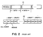
- the pager signal 21 shown in the figure carries a preamble signal and one or more batches succeeding the preamble signal.
- the preamble signal has, for example, an eighteen codeword length.
- a unit codeword consists of, for example, 32 bits.
- the preamble signal is specified by a repetition of pulses which are of logic "1" and "0" levels.
- Each of the batches is shown at 22 in Fig. 2 and consists of, for example, seventeen frames in which codewords SC and CW1 to CW16 are carried.
- Each of the sixteen codewords also consists of 32 bits.
- the codeword SC is a synchronization code signal and succeeds the preamble signal.
- the next succeeding sixteen codewords CW1 through CW16 are classified into eight groups or eight address signals each consisting of a pair of two successive codewords, such as codewords CW1 and CW2 form a group 1, codewords CW3 and CW4 forming another group 2, and codewords CW15 and CW16 forming a group 8.
- a preceding one of the pair of two codewords in one group carries a call number signal and the other carries a message.
- a particular one of the groups in each of the batches is assigned to the pager receiver.
- the pager signal has a predetermined baud rate and is repeatedly transmitted from a base station at predetermined time intervals.
- the decoder comprises a bit synchronization circuit 23, a baud rate monitoring circuit 24, a preamble and synchronization code detection circuit 25, a synchronization controller 26, a call number comparing circuit 28 and a message detection circuit 27.
- the bit synchronization circuit 23 receives the received signal Sd and the reference clock signal RC and produces a reproduced timing signal St.
- the baud rate monitoring circuits 24 receives the received signal Sd, the reference clock signal RC and the reproduced timing signal St and monitors the baud rate of the received signal. When the baud rate monitoring circuit 24 detects that the baud rate of the received signal is equal to the predetermined baud rate, the baud rate monitoring circuit 24 produces a monitoring signal Sr.
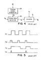
- the baud rate monitoring circuit 24 comprises a window signal generator 29, a rising edge detector 30, and a counter 31.
- the window signal generator 29 receives the reference clock signal RC and produces a window signal Sw which is synchronized with a rising edge of each pulse of the reference clock signal RC as shown in Fig. 5.
- Each pulse of the window signal Sw has a predetermined pulse width smaller than the pulse width of the reference clock signal RC.
- the rising edge detector 30 receives the received signal Sd and the window signal Sw. When detecting that a rising edge of the received signal Sd is timely coincident with one pulse of the window signal Sw, the rising edge detector 30 produces an edge detecting pulse Se as shown in Fig. 5.
- the counter 31 counts the edge detection pulse. When a predetermined value is counted by the counter 31 for a time length equal to one code length, the counter 31 produces a count up signal as the monitoring signal Sr.
- the preamble and synchronization code detection circuit 25 receives the received signal Sd and the reproduced timing signal St.
- the preamble and synchronization code detection circuit 25 detects the preamble signal and the synchronization code signal in the received signal Sd, it produces the preamble detection signal Sp and the synchronization detection signal Ss, respectively.
- the synchronization controller 26 receives the reference clock signal RC, the reproduced timing signal St, the monitoring signal Sr, the preamble detection signal Sp, the synchronization detection signal Ss and the coincident signal Sc and produces a frame timing signal Sf, a group timing signal Sg and a battery saving signal Sb which are collectively shown by a signal Sh in Fig. 3.
- the synchronization controller 26 comprises a controller 32, a bit counter 33, a codeword counter 34, a group timing decision circuit 35, a synchronization code timing decision circuit 36 and an OR circuit 37.
- the controller 32 After receiving one of the monitoring signal Sr and the preamble detection signal Sp, the controller 32 produces a start signal to the bit counter 33 and the codeword counter 34 when it receives the synchronization detection signal Ss.
- the bit counter 33 starts to count the reference clock signal RC.
- the bit counter 33 Upon counting up to thirty-two, the bit counter 33 resets to produce a codeword pulse representative of one codeword. Then, the bit counter 33 again counts the reference clock signal RC.
- the codeword pulse is delivered to the message detection circuit 27 as the frame timing signal Sf.
- the codeword counter 34 starts to count the codeword pulse. Upon counting up to seventeen pulses, the codeword counter 34 resets and again counts the codeword pulse from the bit counter 33. A counted number in the code word counter 34 is supplied to the group timing decision circuit 35. The group timing decision circuit 35 decides a group timing of the particular group assigned to the pager receiver from the counted number in the codeword counter 34 to produce the group timing signal Sg.
- the message detection circuit 27 receives the received signal Sd, the reproduced timing signal St, and the frame timing signal Sf and derives a codeword in each of frames of the received signal.
- the call number comparing circuit 28 receives the received signal Sd, the reproduced timing signal St, the group timing signal Sg and the particular call number Sn, and compares the call number signal in the particular group in the received signal with the particular call number Sn. Upon detecting that the both of them are coincident with each other, the call number comparing circuit 28 produces the coincident signal Sc.
- the processor 15 reads the content in the message detection circuit 27 in response to the coincident signal Sc. At that time, the message detection circuit 27 detects the codeword carrying the message in the particular group. Accordingly, the processor 15 can take out the message addressed to the pager receiver.
- the above-described operation is repeatedly performed for each of the batches in the pager signal.
- the pager receiver uses a battery as an electric power source and the power saving technique in order to strictly restrict consumption of electric power of the battery.
- the controller 32 repeatedly produces a power-on signal at time intervals to the receiving circuit 12.
- the receiving circuit 12 is only supplied with the power from the battery during a time duration of the power-on signal when the pager signal is not transmitted from the base station.
- the time duration of the power-on signal is called a power-on duration.
- the controller 32 When the receiving circuit 12 receives the pager signal during the power-on duration and when the controller 32 receives one of the monitoring signal Sr and the preamble detection signal Sp, the controller 32 continues the power-on signal to extend the power-on duration. Thereafter, when the controller 32 receives the synchronization detection signal Ss, the controller 32 stops the power-on signal. Thereafter, the group timing signal Sg is delivered as another power-on signal to the receiving circuit 12 from the group timing decision circuit 35 through the OR circuit 37. When receiving the coincident signal Sc, the controller 32 again produces the power-on signal. Thus, the receiving circuit 12 can receive the particular group of the pager signal.
- the synchronization code timing decision circuit 36 (Fig. 6) receives the content of the codeword counter 34 and decides a timing of the synchronization codeword from the content to produce a synchronization timing signal.
- the synchronization timing signal is supplied as a further power-on signal to the receiving circuit 12. Therefore, the receiving circuit 12 can receive the synchronization codeword SC in each of the batches in the pager signal.
- a time chart of the battery saving signal is shown at Sb in relation to the pager signal 21.
- power-on signals 38, 39, and 40 are for receiving the first synchronization codeword SC after detection of the preamble, for receiving the particular group, and for receiving the synchronization codeword SC in each of the batches in the pager signal 21.
- the power-on signal 40 is repeatedly produced for receiving the synchronization codeword in each of the batches of the pager signal in order to detect stop of the pager signal.
- the power-on signals 40 When the power-on signals 40 are omitted, stop of the pager signals cannot be detected. Therefore, the power-on signal for receiving the particular group is repeatedly generated after stop of the pager signal. As a result, the receiving circuit 12 receives a noise or any other signals. When the noise or the other signals are coincident with the particular call number Sn, the call number comparing circuit 28 erroneously produces the coincident signal Sc. As a result, the speaker 18 and the light indicator 19 are erroneously driven.
- the pager receiver according to an embodiment of the present invention comprises similar parts to the known pager receiver in Fig. 1 except a decision circuit 41. Similar portions are represented by the same reference symbols in Fig. 1.
- the decision circuit 41 is coupled to the decoder 13, in detail to the baud rate monitoring circuit 24 and the call number comparing circuit 28 as shown in Fig. 3.
- decision circuit 41 receives the monitoring signal Sr and the coincident signal Sc at a time, the decision circuit 41 produces an acceptance signal So.
- the processor 15 receives the acceptance signal So, the processor 15 drives the speaker 18 and the light indicator 19 and takes the message thereinto from the message detection circuit 27 (Fig. 3).
- an example of the decision circuit 41 is an AND gate 42.
- the AND gate 42 has two input terminals for receiving the monitoring signal Sr and the coincident signal Sc, respectively, and an output terminal for producing the acceptance signal So.
- the decision circuit 41 is alternatively composed of a signal processing unit having a decision program for deciding that both of the monitoring signal Sr and the coincident signal Sc are present at a time.
- step 43 it is detected whether or not the coincident signal Sc is present.
- step 44 it is detected whether or not the monitoring signal Sr is present.
- the acceptance signal So is produced at next step 45.
- the processor 15 starts its operation in response to the acceptance signal from the decision circuit 41. Accordingly, even if the coincident signal Sc is erroneously produced from the decoder 13 due to noise after the pager signal stops, the processor 15 is prevented from the erroneous operation because the monitoring signal Sr is not present. Accordingly, the battery saving signal Sb' in Fig. 7 can be employed.
- an example of the synchronization controller 26 for producing the battery saving signal Sb' is similar to the synchronization controller of Fig. 6.
- the similar portions are represented by the same reference symbols.
- the synchronization controller of Fig. 11 does not have the synchronization codeword timing decision circuit (36 in Fig. 6) and therefore produces no power-on signal 40 for receiving the synchronization codeword SC.
- the controller 32 decides stop of the pager signal when receiving no monitoring signal Sr for a predetermined time length and stops operation of the bit counter 33 and the codeword counter 34.
Landscapes
- Engineering & Computer Science (AREA)
- Computer Networks & Wireless Communication (AREA)
- Signal Processing (AREA)
- Mobile Radio Communication Systems (AREA)
Claims (4)
- Rufempfänger zum Empfangen eines Rufsignals mit einer vorgegebenen Baudrate, wobei das Rufsignal ein Präambelsignal und ein oder mehrere dem Präambelsignal folgende Blocksignale aufweist, wobei jedes der Blocksignale ein Synchronisierungscodesignal und mehrere dem Synchronisierungscodesignal folgende Adressensignale aufweist und jedes der Adressensignale ein eine Rufnummer darstellendes Rufnummersignal und ein eine Nachricht darstellendes Nachrichtensignal aufweist, wobei ein bestimmtes der Adressensignale dem Rufempfänger zugewiesen ist,
wobei der Rufempfänger aufweist:eine Empfangseinrichtung (12) zum Empfangen des Rufsignals, um ein Empfangssignal zu erzeugen, wenn Einschaltsignale eines Batteriesparsignals zugeführt werden;eine mit der Empfangseinrichtung verbundene Baudratenüberwachungseinrichtung (24) zum Überwachen einer Baudrate des Empfangssignals, um ein Überwachungssignal (Sr) zu erzeugen, wenn die Baudrate einer vorgegebenen Baudrate gleich ist;eine mit der Empfangseinrichtung verbundene Entnahmeeinrichtung (27) zum Entnehmen eines Nachrichtensignals aus dem Empfangssignal als entnommenes Nachrichtensignal (Sm);eine Speichereinrichtung (16) zum Speichern einer dem Rufempfänger zugeordneten bestimmten Rufnummer (Sn);eine mit der Empfangseinrichtung und der Speichereinrichtung verbundene Einrichtung (28) zum Vergleichen von Rufnummern zum Vergleichen der durch die Rufnummer im Empfangssignal dargestellten Rufnummer mit der bestimmten Rufnummer, um ein Koinzidenzsignal (Sc) zu erzeugen, wenn die Rufnummer und die bestimmte Rufnummer miteinander übereinstimmen;eine mit der Empfangseinrichtung verbundene Präambelerfassungseinrichtung (25) zum Erfassen des Präambelsignals im Empfangssignal, um ein Präambelerfassungssignal (Sp) zu erzeugen;eine mit der Empfangseinrichtung verbundene Synchronisierungscodeerfassungseinrichtung (25) zum Erfassen des Synchronisierungscodesignals (SC) in jedem der Blocksignale des Empfangssignals, um ein Synchronisierungserfassungssignal (Ss) zu erzeugen;eine Batteriesparsignalerzeugungseinrichtung (26) ;eine mit der Baudratenüberwachungseinrichtung und der Einrichtung zum Vergleichen von Rufnummern verbundene Entscheidungseinrichtung (41), durch die festgestellt wird, ob das Überwachungssignal (Sr) und das Koinzidenzsignal (Sc) vorhanden sind oder nicht, um ein Annahmesignal zu erzeugen, wenn sowohl das Überwachungssignal als auch das Koinzidenzsignal vorhanden sind; undeine mit der Entscheidungseinrichtung und der Entnahmeeinrichtung verbundene und auf das Annahmesignal ansprechende Verarbeitungseinrichtung (15), die das entnommene Nachrichtensignal übernimmt;dadurch gekennzeichnet, daß
die Batteriesparsignalerzeugungseinrichtung (26) mit der Baudratenüberwachungseinrichtung (24), der Präambelerfassungseinrichtung (25) und der Synchronisierungscodeerfassungseinrichtung (25) verbunden ist, um eines der Einschaltsignale (38) des Batteriesparsignals (Sb') während einer Zeitdauer vom Empfang des Überwachungssignals (Sr) oder des Präambelerfassungssignals (Sp) bis zum ersten Empfang des Synchronisierungssignals (SC) zu erzeugen und anschließend ein anderes der Einschaltsignale (39) mit einem geeigneten Takt zum Empfangen des bestimmten Adressensignals zu erzeugen. - Rufempfänger nach Anspruch 1, wobei die Entscheidungseinrichtung (41) eine UND-Schaltung (42) mit zwei Eingangsanschlüssen, die mit der Baudratenüberwachungsschaltung bzw. der Einrichtung zum Vergleichen von Rufnummern verbunden sind, und einem Ausgangsanschluß zum Erzeugen des Annahmesignals ist.
- Rufempfänger zum Empfangen eines Rufsignals mit einer bestimmten Baudrate, wobei das Rufsignal ein Präambelsignal und ein oder mehrere dem Präambelsignal folgende Blocksignale aufweist, wobei jedes der Blocksignale ein Synchronisierungscodesignal und mehrere dem Synchronisierungscodesignal folgende Adressensignale aufweist und jedes der Adressensignale ein Rufnummersignal und ein Nachrichtensignal aufweist, wobei ein bestimmtes der Adressensignale dem Rufempfänger zugewiesen ist,
wobei der Rufempfänger aufweist:eine Empfangseinrichtung (12) zum Empfangen des Rufsignals, um ein Empfangssignal zu erzeugen, wenn Einschaltsignale (38) eines Batteriesparsignals (Sb') zugeführt werden;eine mit der Empfangseinrichtung verbundene Baudratenüberwachungseinrichtung (24) zum Überwachen einer Baudrate des Empfangssignals, um ein Überwachungssignal (Sr) zu erzeugen, wenn die Baudrate einer vorgegebenen Baudrate gleich ist;eine mit der Empfangseinrichtung verbundene Präambelerfassungseinrichtung (25) zum Erfassen des Präambelsignals im Empfangssignal, um ein Präambelerfassungssignal (Sp) zu erzeugen;eine mit der Empfangseinrichtung verbundene Synchronisierungscodeerfassungseinrichtung (25) zum Erfassen des Synchronisierungscodesignals in jedem der Blocksignale des Empfangssignals, um ein Synchronisierungserfassungssignal (Ss) zu erzeugen;eine Referenztakteinrichtung (14) zum Erzeugen eines Referenztaktsignals;eine mit der Empfangseinrichtung verbundene Entnahmeeinrichtung (27) zum Entnehmen eines Nachrichtensignals aus dem Empfangssignal als entnommenes Nachrichtensignal;eine Speichereinrichtung (16) zum Speichern einer dem Rufempfänger zugeordneten bestimmten Rufnummer (Sn);eine mit einer Schaltung zum Festlegen eines bestimmten Adressentaktes, der Empfangseinrichtung und der Speichereinrichtung verbundene Einrichtung (28) zum Vergleichen von Rufnummern zum Vergleichen der durch die Rufnummer im bestimmten Adressensignal im Empfangssignal dargestellten Rufnummer mit der bestimmten Rufnummer, um ein Koinzidenzsignal zu erzeugen, wenn die Rufnummer im bestimmten Adressensignal und die bestimmte Rufnummer miteinander übereinstimmen;eine mit der Baudratenüberwachungseinrichtung und der Einrichtung zum Vergleichen von Rufnummern verbundene Entscheidungseinrichtung (41), durch die festgestellt wird, ob das Überwachungssignal und das Koinzidenzsignal vorhanden sind oder nicht, um ein Annahmesignal zu erzeugen, wenn sowohl das Überwachungssignal als auch das Koinzidenzsignal vorhanden sind; undeine mit der Entscheidungseinrichtung und der Entnahmeeinrichtung verbundene und auf das Annahmesignal ansprechende Verarbeitungseinrichtung (15), die das entnommene Nachrichtensignal übernimmt;gekennzeichnet durcheine mit der Baudratenüberwachungseinrichtung, der Präambelerfassungseinrichtung und der Synchronisierungscodeerfassungseinrichtung verbundene Erzeugungseinrichtung (26) zum Erzeugen eines der Einschaltsignale während einer Zeitdauer vom Empfang des Überwachungssignals oder des Präambelerfassungssignals bis zum ersten Empfang des Synchronisierungserfassungssignals; unddie mit der Synchronisierungscodeerfassungseinrichtung und der Referenztakteinrichtung verbundene Schaltung (28) zum Festlegen eines bestimmten Adressentaktes zum Festlegen eines Taktes zum Empfangen des bestimmten Adressensignals auf der Basis des Synchronisierungserfassungssignals und des Referenztaktsignals, um ein Taktsignal für die bestimmte Adresse zu erzeugen, das der Empfangseinrichtung als eines der Einschaltsignale des Batteriesparsignals zugeführt wird. - Rufempfänger nach Anspruch 3, wobei die Entscheidungseinrichtung (41) eine UND-Schaltung (42) mit zwei Eingangsanschlüssen, die mit der Baudratenüberwachungseinrichtung bzw. mit der Einrichtung zum Vergleichen von Rufnummern verbunden sind, und einem Ausgangsanschluß zum Erzeugen des Annahmesignals ist.
Applications Claiming Priority (2)
| Application Number | Priority Date | Filing Date | Title |
|---|---|---|---|
| JP285753/90 | 1990-10-25 | ||
| JP2285753A JP2646831B2 (ja) | 1990-10-25 | 1990-10-25 | 選択呼出受信機 |
Publications (3)
| Publication Number | Publication Date |
|---|---|
| EP0482632A2 EP0482632A2 (de) | 1992-04-29 |
| EP0482632A3 EP0482632A3 (en) | 1993-04-28 |
| EP0482632B1 true EP0482632B1 (de) | 1997-08-06 |
Family
ID=17695604
Family Applications (1)
| Application Number | Title | Priority Date | Filing Date |
|---|---|---|---|
| EP91118145A Expired - Lifetime EP0482632B1 (de) | 1990-10-25 | 1991-10-24 | Rufempfänger der das Auslassen des Spannungsanschaltsignals erlaubt für den Empfang des Synchronisierungskodes im Rufsignal |
Country Status (6)
| Country | Link |
|---|---|
| US (1) | US5296849A (de) |
| EP (1) | EP0482632B1 (de) |
| JP (1) | JP2646831B2 (de) |
| AU (1) | AU647194B2 (de) |
| CA (1) | CA2054107C (de) |
| DE (1) | DE69127159T2 (de) |
Families Citing this family (45)
| Publication number | Priority date | Publication date | Assignee | Title |
|---|---|---|---|---|
| US20010050943A1 (en) * | 1989-08-03 | 2001-12-13 | Mahany Ronald L. | Radio frequency communication network having adaptive communication parameters |
| US7606575B2 (en) * | 1988-08-04 | 2009-10-20 | Broadcom Corporation | Remote radio data communication system with data rate switching |
| JPH04328919A (ja) * | 1991-04-26 | 1992-11-17 | Fujitsu Ltd | 無線呼出し信号方式 |
| US7415548B2 (en) | 1991-05-13 | 2008-08-19 | Broadcom Corporation | Communication network having a plurality of bridging nodes which transmits a polling message with backward learning technique to determine communication pathway |
| US7558557B1 (en) * | 1991-11-12 | 2009-07-07 | Broadcom Corporation | Low-power messaging in a network supporting roaming terminals |
| US6374311B1 (en) | 1991-10-01 | 2002-04-16 | Intermec Ip Corp. | Communication network having a plurality of bridging nodes which transmit a beacon to terminal nodes in power saving state that it has messages awaiting delivery |
| WO1993007691A1 (en) * | 1991-10-01 | 1993-04-15 | Norand Corporation | A radio frequency local area network |
| US6407991B1 (en) * | 1993-05-06 | 2002-06-18 | Intermec Ip Corp. | Communication network providing wireless and hard-wired dynamic routing |
| US5487090A (en) * | 1992-10-12 | 1996-01-23 | Nec Corporation | Selectively called radio receiver in which bit rate detection is controlled with a predetermined range |
| US7917145B2 (en) * | 1992-11-02 | 2011-03-29 | Broadcom Corporation | Radio frequency local area network |
| JP2773584B2 (ja) * | 1992-11-04 | 1998-07-09 | 日本電気株式会社 | 無線選択呼び出し受信機 |
| JPH0795142A (ja) * | 1993-09-20 | 1995-04-07 | Fujitsu Ltd | スター型ネットワーク用親局端局装置 |
| US5563910A (en) * | 1993-11-12 | 1996-10-08 | Motorola, Inc. | Recursive baud rate detection method and apparatus |
| JP2630233B2 (ja) * | 1993-12-16 | 1997-07-16 | 日本電気株式会社 | バッテリーセービング機能をもつ無線選択呼出受信機 |
| WO1995024081A1 (en) | 1994-03-03 | 1995-09-08 | Proxim, Inc. | Frequency hopping medium access control protocol |
| US6292508B1 (en) | 1994-03-03 | 2001-09-18 | Proxim, Inc. | Method and apparatus for managing power in a frequency hopping medium access control protocol |
| US5537100A (en) * | 1994-04-06 | 1996-07-16 | Sharp Microelectronics Technology, Inc. | System and method for analyzing coded transmission sent to mobile message receivers |
| US5581803A (en) * | 1994-04-21 | 1996-12-03 | Motorola, Inc. | Method of programming a radio identification code in a communication unit |
| US5497145A (en) * | 1994-07-05 | 1996-03-05 | Motorola, Inc. | Selective call receiver with battery saving features and method therefor |
| KR100201806B1 (ko) * | 1994-10-19 | 1999-06-15 | 윤종용 | 무선호출수신기의전원 절약장치 및 방법 |
| GB2297884B (en) * | 1995-02-07 | 1999-05-26 | Nokia Mobile Phones Ltd | Radio telephone |
| JP2692630B2 (ja) * | 1995-02-09 | 1997-12-17 | 日本電気株式会社 | 無線選択呼出受信機 |
| JP3424379B2 (ja) * | 1995-03-30 | 2003-07-07 | カシオ計算機株式会社 | 選択呼出受信装置 |
| US5721744A (en) * | 1996-02-20 | 1998-02-24 | Sharp Microelectronics Technology, Inc. | System and method for correcting burst errors in digital information |
| US5978379A (en) | 1997-01-23 | 1999-11-02 | Gadzoox Networks, Inc. | Fiber channel learning bridge, learning half bridge, and protocol |
| US7430171B2 (en) | 1998-11-19 | 2008-09-30 | Broadcom Corporation | Fibre channel arbitrated loop bufferless switch circuitry to increase bandwidth without significant increase in cost |
| US6911855B2 (en) * | 1999-06-28 | 2005-06-28 | Broadcom Corporation | Current-controlled CMOS circuit using higher voltage supply in low voltage CMOS process |
| US6424194B1 (en) * | 1999-06-28 | 2002-07-23 | Broadcom Corporation | Current-controlled CMOS logic family |
| US6897697B2 (en) * | 1999-06-28 | 2005-05-24 | Broadcom Corporation | Current-controlled CMOS circuit using higher voltage supply in low voltage CMOS process |
| US6424177B1 (en) * | 1999-06-28 | 2002-07-23 | Broadcom Corporation | Universal single-ended parallel bus |
| US6340899B1 (en) | 2000-02-24 | 2002-01-22 | Broadcom Corporation | Current-controlled CMOS circuits with inductive broadbanding |
| US7546141B2 (en) * | 2000-05-23 | 2009-06-09 | Robert Leon | Hybrid communication system and method |
| US6864558B2 (en) * | 2001-05-17 | 2005-03-08 | Broadcom Corporation | Layout technique for C3MOS inductive broadbanding |
| US7212534B2 (en) | 2001-07-23 | 2007-05-01 | Broadcom Corporation | Flow based congestion control |
| US6624699B2 (en) * | 2001-10-25 | 2003-09-23 | Broadcom Corporation | Current-controlled CMOS wideband data amplifier circuits |
| US7295555B2 (en) * | 2002-03-08 | 2007-11-13 | Broadcom Corporation | System and method for identifying upper layer protocol message boundaries |
| US7934021B2 (en) * | 2002-08-29 | 2011-04-26 | Broadcom Corporation | System and method for network interfacing |
| US7346701B2 (en) * | 2002-08-30 | 2008-03-18 | Broadcom Corporation | System and method for TCP offload |
| US8180928B2 (en) | 2002-08-30 | 2012-05-15 | Broadcom Corporation | Method and system for supporting read operations with CRC for iSCSI and iSCSI chimney |
| EP1554842A4 (de) * | 2002-08-30 | 2010-01-27 | Corporation Broadcom | System und verfahren zum behandeln von ausserhalb der reihenfolge auftretenden rahmen |
| US7313623B2 (en) * | 2002-08-30 | 2007-12-25 | Broadcom Corporation | System and method for TCP/IP offload independent of bandwidth delay product |
| US7598811B2 (en) * | 2005-07-29 | 2009-10-06 | Broadcom Corporation | Current-controlled CMOS (C3MOS) fully differential integrated wideband amplifier/equalizer with adjustable gain and frequency response without additional power or loading |
| US7362174B2 (en) * | 2005-07-29 | 2008-04-22 | Broadcom Corporation | Current-controlled CMOS (C3MOS) wideband input data amplifier for reduced differential and common-mode reflection |
| US7598788B2 (en) * | 2005-09-06 | 2009-10-06 | Broadcom Corporation | Current-controlled CMOS (C3MOS) fully differential integrated delay cell with variable delay and high bandwidth |
| US7450944B2 (en) * | 2005-11-03 | 2008-11-11 | Motorola, Inc. | Method and apparatus for base station synchronization |
Family Cites Families (7)
| Publication number | Priority date | Publication date | Assignee | Title |
|---|---|---|---|---|
| GB2103402B (en) * | 1981-07-27 | 1984-09-05 | Standard Telephones Cables Ltd | Synchronisation of digital radio pager |
| GB8320979D0 (en) * | 1983-08-03 | 1983-09-07 | Multitone Electronics Plc | Decoding arrangements |
| KR950011489B1 (ko) * | 1986-10-21 | 1995-10-05 | 모토로라 인코포레이티드 | 선택 호출 무선 수신기 및 그의 동작 방법 |
| JPH01190054A (ja) * | 1988-01-25 | 1989-07-31 | Man Design Kk | 受信機 |
| US4996526A (en) * | 1988-12-01 | 1991-02-26 | Motorola, Inc. | Power conservation method and apparatus for a portion of a synchronous information signal |
| JP2893591B2 (ja) * | 1989-03-31 | 1999-05-24 | カシオ計算機株式会社 | 選択呼出方式及び受信方式並びに受信機 |
| US5049875A (en) * | 1989-09-13 | 1991-09-17 | Motorola Inc. | Method and apparatus for out of range detection in response to nondetection of predetermined baud rates |
-
1990
- 1990-10-25 JP JP2285753A patent/JP2646831B2/ja not_active Expired - Fee Related
-
1991
- 1991-10-24 EP EP91118145A patent/EP0482632B1/de not_active Expired - Lifetime
- 1991-10-24 DE DE69127159T patent/DE69127159T2/de not_active Expired - Fee Related
- 1991-10-24 CA CA002054107A patent/CA2054107C/en not_active Expired - Fee Related
- 1991-10-25 US US07/782,829 patent/US5296849A/en not_active Expired - Fee Related
- 1991-10-25 AU AU86775/91A patent/AU647194B2/en not_active Ceased
Also Published As
| Publication number | Publication date |
|---|---|
| CA2054107A1 (en) | 1992-04-26 |
| DE69127159T2 (de) | 1997-12-18 |
| DE69127159D1 (de) | 1997-09-11 |
| JPH04160823A (ja) | 1992-06-04 |
| EP0482632A2 (de) | 1992-04-29 |
| US5296849A (en) | 1994-03-22 |
| CA2054107C (en) | 1996-04-02 |
| EP0482632A3 (en) | 1993-04-28 |
| AU8677591A (en) | 1992-04-30 |
| JP2646831B2 (ja) | 1997-08-27 |
| AU647194B2 (en) | 1994-03-17 |
Similar Documents
| Publication | Publication Date | Title |
|---|---|---|
| EP0482632B1 (de) | Rufempfänger der das Auslassen des Spannungsanschaltsignals erlaubt für den Empfang des Synchronisierungskodes im Rufsignal | |
| US5230084A (en) | Selective call receiver having extended battery saving capability | |
| US4663623A (en) | Decoding arrangements for synchronous receivers | |
| EP0091695B1 (de) | Stromsparschaltung für einen Rufempfänger | |
| EP0071425B1 (de) | Synchronisation eines drahtlosen digitalen Selektivrufempfängers | |
| US4652875A (en) | Pager with improved battery saving function | |
| US4961073A (en) | Battery saving apparatus and method providing optimum synchronization codeword detection | |
| US4803703A (en) | Apparatus and method for fine synchronization of a communication receiver | |
| US5537100A (en) | System and method for analyzing coded transmission sent to mobile message receivers | |
| EP0118153B1 (de) | Dekodiersystem für einen Personenrufempfänger | |
| EP0597308A2 (de) | Methode zur Senkung der Energieverbrauchs in Batterie-betriebenen Funkrufempfängern | |
| KR860001439B1 (ko) | 디지탈 무선 페이징 수신기용 신호검출회로 | |
| US6216385B1 (en) | Radio calling receiver with means to control reception based on service area, time zone, and/or electric field strength | |
| US5487090A (en) | Selectively called radio receiver in which bit rate detection is controlled with a predetermined range | |
| CA1209643A (en) | Digital radio paging receiver | |
| US5497145A (en) | Selective call receiver with battery saving features and method therefor | |
| EP0649209B1 (de) | Stromversorgungsregelung für einen Empfänger | |
| EP0465463B1 (de) | Gerät und verfahren zur energiekonservierung für einen teil eines bestimmten signals | |
| US5821873A (en) | Method and apparatus for saving power in a selective call receiver | |
| US5526368A (en) | Method for receiving calling data even if missing a predetermined code in a paging receiver | |
| GB2136179A (en) | Pager Decoding System | |
| EP0372473B1 (de) | Funkrufempfänger | |
| KR860000978B1 (ko) | 디지탈 무선 페이징 수신기 | |
| KR0130629B1 (ko) | 다중경보 수신기에서의 프리앰블 포착 실패시에도 호 데이타를 수신할 수 있는 방법 | |
| JPH0226137A (ja) | 無線呼出受信機 |
Legal Events
| Date | Code | Title | Description |
|---|---|---|---|
| PUAI | Public reference made under article 153(3) epc to a published international application that has entered the european phase |
Free format text: ORIGINAL CODE: 0009012 |
|
| 17P | Request for examination filed |
Effective date: 19911119 |
|
| AK | Designated contracting states |
Kind code of ref document: A2 Designated state(s): DE GB NL |
|
| PUAL | Search report despatched |
Free format text: ORIGINAL CODE: 0009013 |
|
| AK | Designated contracting states |
Kind code of ref document: A3 Designated state(s): DE GB NL |
|
| 17Q | First examination report despatched |
Effective date: 19950726 |
|
| GRAG | Despatch of communication of intention to grant |
Free format text: ORIGINAL CODE: EPIDOS AGRA |
|
| GRAH | Despatch of communication of intention to grant a patent |
Free format text: ORIGINAL CODE: EPIDOS IGRA |
|
| GRAH | Despatch of communication of intention to grant a patent |
Free format text: ORIGINAL CODE: EPIDOS IGRA |
|
| GRAA | (expected) grant |
Free format text: ORIGINAL CODE: 0009210 |
|
| AK | Designated contracting states |
Kind code of ref document: B1 Designated state(s): DE GB NL |
|
| REF | Corresponds to: |
Ref document number: 69127159 Country of ref document: DE Date of ref document: 19970911 |
|
| PLBE | No opposition filed within time limit |
Free format text: ORIGINAL CODE: 0009261 |
|
| STAA | Information on the status of an ep patent application or granted ep patent |
Free format text: STATUS: NO OPPOSITION FILED WITHIN TIME LIMIT |
|
| 26N | No opposition filed | ||
| PGFP | Annual fee paid to national office [announced via postgrant information from national office to epo] |
Ref country code: NL Payment date: 20001026 Year of fee payment: 10 |
|
| REG | Reference to a national code |
Ref country code: GB Ref legal event code: IF02 |
|
| PG25 | Lapsed in a contracting state [announced via postgrant information from national office to epo] |
Ref country code: NL Free format text: LAPSE BECAUSE OF NON-PAYMENT OF DUE FEES Effective date: 20020501 |
|
| NLV4 | Nl: lapsed or anulled due to non-payment of the annual fee |
Effective date: 20020501 |
|
| PGFP | Annual fee paid to national office [announced via postgrant information from national office to epo] |
Ref country code: GB Payment date: 20041020 Year of fee payment: 14 |
|
| PGFP | Annual fee paid to national office [announced via postgrant information from national office to epo] |
Ref country code: DE Payment date: 20041021 Year of fee payment: 14 |
|
| PG25 | Lapsed in a contracting state [announced via postgrant information from national office to epo] |
Ref country code: GB Free format text: LAPSE BECAUSE OF NON-PAYMENT OF DUE FEES Effective date: 20051024 |
|
| PG25 | Lapsed in a contracting state [announced via postgrant information from national office to epo] |
Ref country code: DE Free format text: LAPSE BECAUSE OF NON-PAYMENT OF DUE FEES Effective date: 20060503 |
|
| GBPC | Gb: european patent ceased through non-payment of renewal fee |
Effective date: 20051024 |