EP0483246B1 - Circuit electrique combinant une alimentation polarisee et un dispositif de coupure - Google Patents
Circuit electrique combinant une alimentation polarisee et un dispositif de coupure Download PDFInfo
- Publication number
- EP0483246B1 EP0483246B1 EP90911516A EP90911516A EP0483246B1 EP 0483246 B1 EP0483246 B1 EP 0483246B1 EP 90911516 A EP90911516 A EP 90911516A EP 90911516 A EP90911516 A EP 90911516A EP 0483246 B1 EP0483246 B1 EP 0483246B1
- Authority
- EP
- European Patent Office
- Prior art keywords
- current
- microcircuit
- circuit
- voltage
- bias
- Prior art date
- Legal status (The legal status is an assumption and is not a legal conclusion. Google has not performed a legal analysis and makes no representation as to the accuracy of the status listed.)
- Expired - Lifetime
Links
- 230000009977 dual effect Effects 0.000 abstract 1
- 238000000034 method Methods 0.000 description 7
- 238000010586 diagram Methods 0.000 description 5
- VYPSYNLAJGMNEJ-UHFFFAOYSA-N Silicium dioxide Chemical compound O=[Si]=O VYPSYNLAJGMNEJ-UHFFFAOYSA-N 0.000 description 2
- 230000008901 benefit Effects 0.000 description 2
- 230000001419 dependent effect Effects 0.000 description 2
- 238000002955 isolation Methods 0.000 description 2
- ZMHWQAHZKUPENF-UHFFFAOYSA-N 1,2-dichloro-3-(4-chlorophenyl)benzene Chemical compound C1=CC(Cl)=CC=C1C1=CC=CC(Cl)=C1Cl ZMHWQAHZKUPENF-UHFFFAOYSA-N 0.000 description 1
- 230000002411 adverse Effects 0.000 description 1
- 230000015556 catabolic process Effects 0.000 description 1
- 239000004020 conductor Substances 0.000 description 1
- 238000007796 conventional method Methods 0.000 description 1
- 230000001351 cycling effect Effects 0.000 description 1
- 230000007423 decrease Effects 0.000 description 1
- 238000006731 degradation reaction Methods 0.000 description 1
- 238000009792 diffusion process Methods 0.000 description 1
- 239000011159 matrix material Substances 0.000 description 1
- 229910021420 polycrystalline silicon Inorganic materials 0.000 description 1
- 230000002441 reversible effect Effects 0.000 description 1
- 230000035945 sensitivity Effects 0.000 description 1
- 235000012239 silicon dioxide Nutrition 0.000 description 1
- 239000000377 silicon dioxide Substances 0.000 description 1
Images


Classifications
-
- H—ELECTRICITY
- H04—ELECTRIC COMMUNICATION TECHNIQUE
- H04W—WIRELESS COMMUNICATION NETWORKS
- H04W52/00—Power management, e.g. Transmission Power Control [TPC] or power classes
- H04W52/02—Power saving arrangements
- H04W52/0209—Power saving arrangements in terminal devices
- H04W52/0261—Power saving arrangements in terminal devices managing power supply demand, e.g. depending on battery level
- H04W52/0274—Power saving arrangements in terminal devices managing power supply demand, e.g. depending on battery level by switching on or off the equipment or parts thereof
- H04W52/028—Power saving arrangements in terminal devices managing power supply demand, e.g. depending on battery level by switching on or off the equipment or parts thereof switching on or off only a part of the equipment circuit blocks
-
- Y—GENERAL TAGGING OF NEW TECHNOLOGICAL DEVELOPMENTS; GENERAL TAGGING OF CROSS-SECTIONAL TECHNOLOGIES SPANNING OVER SEVERAL SECTIONS OF THE IPC; TECHNICAL SUBJECTS COVERED BY FORMER USPC CROSS-REFERENCE ART COLLECTIONS [XRACs] AND DIGESTS
- Y02—TECHNOLOGIES OR APPLICATIONS FOR MITIGATION OR ADAPTATION AGAINST CLIMATE CHANGE
- Y02D—CLIMATE CHANGE MITIGATION TECHNOLOGIES IN INFORMATION AND COMMUNICATION TECHNOLOGIES [ICT], I.E. INFORMATION AND COMMUNICATION TECHNOLOGIES AIMING AT THE REDUCTION OF THEIR OWN ENERGY USE
- Y02D30/00—Reducing energy consumption in communication networks
- Y02D30/70—Reducing energy consumption in communication networks in wireless communication networks
Definitions
- the present invention relates to electronic circuitry and more particularly to power shut-off circuitry and to current bias circuitry.
- Electronic paging systems incorporating portable, battery operated paging receivers use various methods for reducing the power consumption of the receivers to minimize their overall size and to extend battery life.
- Many of the existing systems supply power to the receiver circuits only during intermittent and/or predetermined time periods during which data for the receiver is transmitted.
- the problem of limiting power consumption and extending battery life is exacerbated in miniature radio receivers incorporated in a wristwatch-pager such as that described in US-A-4,713,808.
- a conventional method for switching power to a circuit utilizes a switching device such as a series pass transistor; however, there are several disadvantages associated with such circuits.
- a series pass device in the on state, has an associated voltage drop that subtracts from the available supply voltage. Such voltage drop is significant in low-voltage, battery operated apparatus.
- the current must be consumed in the controlling element of a power switching device, e.g., the base current required to saturate a switching transistor is greater than the collector current divided by beta.
- the base current of the switching device can be a significant percentage of the total current, and this current is essentially wasted.
- Another disadvantage of using a series switching devices is that the die area required for a switching device that carries the total chip current is significant.
- a separate, off-chip switching transistor could be used to improve beta at the cost of an additional part and more board area.
- An npn switching device could be used to reduce the base current demand, but such a device would require a base voltage above the battery voltage for a low collector-emitter voltage C CE drop if the switching device were placed between the battery positive terminal and the load. It is noted that if a pass device were placed in the ground return path, its V CE drop could adversely affect ground-referenced signals.
- EP-A-0173367 discloses a battery economising circuit comprising a voltage source terminal for supplying and operating voltage, a functional circuit connected to the voltage source terminal, bias generating means connected to the voltage source terminal for generating a bias current for operating the functional circuit and disabling means for disabling the bias current generating means thereby shutting off the bias current to the functional circuit, whereby power dissipation in the microcircuit is limited to leakage currents from the circuit elements of the functional circuit.
- the object of the present invention is to provide an improved on-off switching circuit that maximizes battery life.
- Another object of the present invention is to eliminate the need for a series switching device and thereby eliminate the voltage drop normally associated with such a device.
- Yet another object of the present invention is to provide an on-off switch for electronic circuitry which requires little or no power in the off state.
- Another object of the instant invention is to provide an improved microcircuit bias supply with on-off switching control that results in virtually zero circuit drain from the circuits during quiescent periods.
- the present invention provides a microcircuit comprising a voltage source terminal for supplying an operating voltage to the microcircuit elements; a functional circuit connected to the voltage source terminal and including a plurality of microcircuit elements; bias current generating means connected to the voltage source terminal for generating a bias current for operating the functional circuit; and disabling means for disabling the bias current generating means thereby shutting off the bias current to the functional circuit; whereby power dissipation in the microcircuit is limited to leakage currents of the plurality of microcircuit elements; characterised in that the bias current generating means comprises a first current source connected to the voltage source terminal for generating a reference current; a circuit for receiving the reference current and generating a reference voltage; a second current source coupled to the functional circuits and referenced to the reference voltage, the second current source generating the bias current.
- the present invention also provides a microcircuit comprising a voltage source terminal supplying an operating voltage to the microcircuit; a functional circuit connected to the voltage source terminal, the functional circuit including a plurality of microcircuit elements and a plurality of corresponding first current mirror circuits; means for switching the bias-current circuit to a quiescent state thereby disabling the plurality of microcircuit elements, whereby power dissipation in the microcircuit is limited to leakage currents of the microcircuit elements; characterised in that the bias-current circuit comprising a first current source connected to the voltage source terminal and generating a reference current; a reference-voltage circuit receiving the reference current and generating a reference voltage; a plurality of second current sources corresponding with the plurality of microcircuit elements, each of the plurality of second current sources being referenced to the reference voltage and each generating a bias current of predetermined magnitude suitable for operating the corresponding one of the plurality of microcircuit element; a plurality of second current-mirror circuits, each connected to a
- the present invention combines in a novel way an on-off switch and the current bias supply circuits for a number of functional circuits.
- a very small supply independent current source is switched by the external on-off signal.
- the switch which controls the small independent current source is configured so that the switch draws no current in the off state.
- the small independent current source in turn controls a temperature stable reference voltage source through a current mirror.
- the output of the reference voltage source controls a plurality of master current sources. These master current sources in turn control functional circuit current bias supplies through current mirrors.
- the major advantages of an embodiment of the present invention is that it draws no current in the "off" state and that it does not have a series switch with the associated voltage drop.
- the functional circuit current bias supply circuits are controlled from the voltage reference through current mirrors and hence they operate at a voltage which is relatively near ground potential. The entire supply voltage (except for the drop across the bias supply circuits) is available to the application circuits.
- FIG. 1 shows a bias circuit 10 supplying bias current to a plurality of system functional circuits 12, which in the presently described embodiment of the invention comprise the bipolar integrated-circuit components of a miniature FM subcarrier receiver in a wristwatch-pager as described in US-A-4,713,808.
- Operating voltage V CC is supplied to the bias circuit 10 and the system circuits 12 directly from a battery 14 on a bus 18; battery voltage is suitably 2.2 to 3.5 volts.
- the system functional circuits 12 of FIG. 1 are shown as a plurality of functional circuit areas 20a..n of an integrated circuit chip 21, which can for example be mounted on a printed circuit board (PCB) 22, the bias circuit 10 being located among the circuit areas 20a..n to allow convenient distribution of bias currents.
- a functional circuit can be any circuit such as a logic gate, an amplifier or a bistable.
- a functional circuit area means a group of microcircuit elements that make up one or more functional circuits that perform a particular function and by design can be conveniently grouped together in a particular area of an integrated circuit die.
- a microcircuit element means an integrated-circuit component such as a resistor or a transistor; a microcircuit means at least one functional circuit on an integrated circuit die and formed from interconnected microcircuit elements.
- Such microcircuit elements could, for example, form a functional circuit area comprising an IF strip, an audio amplifier or a storage matrix. For simplicity, only representative portions of the PCB 22 and the interconnecting conductors are shown.
- Transistor current sources are commonly used in analog integrated circuits as biasing elements, which results in reduced sensitivity of circuit performance to power-supply variations and to temperature. Further, current sources often utilize less die area than resistors to provide the desired bias current, particularly when the required value of bias current is small. As indicated in FIG. 1, when power is enabled in the presently described embodiment of the invention, the system circuits 12 collectively require about 15 milliamps of current. Each of the circuit areas 20a..n is connected internally of the area by a lead 23a..n to a current source 24a..n, one of which is illustrated symbolically in FIG. 1 as one element 24a of a current-mirror circuit 26a.
- Corresponding current-mirror circuits such as the circuit 26a are provided in each of the plurality of circuit areas 20a..n.
- the current source 24a mirrors a second current source 28a of the current-mirror circuit 26a, as described in more detail below.
- Each of the current-mirror circuits 26a..n in the various circuit areas 20a..n is connected by a lead 30a..n to a corresponding current mirror circuit 32a..n in the bias circuit 10.
- Power is applied to the system circuits by way of a power-enable control signal PWRUP1 on a lead 34 from a microprocessor (not shown) that controls system power.
- the PWRUP1 signal is a CMOS digital logic level, which controls a switch circuit 36 in the ground return of a supply-independent current source 38.
- a supply-independent current source is one in which the bias currents of the circuit are dependent on a voltage standard other than the supply voltage, for example a Zener diode or the base-emitter voltage V BE of a transistor.
- the best-mode supply-independent current source is a bootstrap or self-biased current source 38, which develops a current that is made to depend directly on the output of the current source itself, thereby establishing a reference current that is relatively independent of power supply voltage.
- the current developed in the bootstrap current source 38 is mirrored in another current source 39, the current sources 38, 39 together forming a current-mirror circuit 40, the output of which is supplied to a band-gap reference circuit 42.
- the band-gap circuit 42 develops a temperature-stable reference voltage of 1.21 volts, which is distributed to a plurality of master current sources 44a..n in the bias circuit 10.
- Each of the master current sources 44a..n includes an on-chip current-setting resistor 46a..n, and is coupled to a corresponding one of the current-mirror circuits 32a..n.
- the bias circuit 10 is centrally located among the other functional circuit areas 20a..n, and while the band-gap voltage could be distributed to the circuits 20a..n, it would be susceptible to voltage drops from resistance in leads, noise, etc.
- the importance of voltage drops is muted.
- Current sources 32a..n have a high-impedance output, and resistance in the lines 30a..n does not affect the magnitude of the currents.
- the current is again mirrored, in each instance in one of the current mirror circuits 26a..n.
- the bias currents are remotely re-mirrored in the functional circuit areas, it is seen that a bias current could be supplied directly to a functional circuit locally from the bias supply 10, for example by the current source 48.
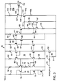
- FIG. 3 a detailed schematic diagram shows the circuits of FIG. 1, which are implemented in a bipolar integrated circuit.
- the switch circuit 36 comprises a substrate-contact diffusion transistor 50 which has good saturation characteristics.
- Transistor 50 has its base connected through a 100K resistor 51 to ground, and through another 100K resistor 52 to the PWRUP1 signal input lead 34.
- the transistor 50 when enabled by the PWRUP1 signal, provides a ground return for the bootstrap current source circuit 38 at a node 56.
- the bootstrap current source 38 comprises a first lateral pnp (LPNP) transistor 57 having its emitter connected through a 1K resistor 58 to the supply voltage V CC , a second LPNP transistor 60 and a diode-connected LPNP transistor 61, each of the latter having an emitter connected through a corresponding 2K resistor 62, 63 to the supply voltage V CC .
- the bases of the transistors 60, 61 are common, and the collector of transistor 60 is connected to the collector of transistor 65 and the base of transistor 57.
- An npn transistor 64 has its collector connected to the base-collector junction of the diode 61, and its emitter connected to the node 56.
- the base of transistor 64 is common with the bases of npn transistors 65, 66, and with a node 67 at the base-emitter junction of a diode-connected npn transistor 68.
- the emitter of transistor 65 is connected through a 650 ohm resistor 69 to the node 56, and the emitters of the transistor 66 and the diode-connected transistor 68 are connected directly to the node 56.
- a startup circuit 70 comprises a 100K resistor 72 connected in series with two diode-connected transistors 73, 74 to ground node 56, and a diode-connected transistor 76 having its emitter connected to a node 77 between the collector of transistor 57 and a 15K resistor 78, which is connected at its other end to the node 67.
- the collector-base junction of the diode 76 is connected to a node 79 between the resistor 72 and the diode 73.
- the bootstrap current source circuit 38 has the potential of operating at two stable states, one in which there is zero current flowing in the circuit, and the other in which equal currents flow through the two branches of the circuit.
- the startup circuit 70 serves to avoid the zero-current state by insuring that some current always flows in the transistors of the circuit 38, and the current gain does not fall to a very low value. If the circuit 38 were near the zero-current state, the voltage at the base of transistor 65 would be at or near ground, and the voltage at the node 67 would be slightly above ground as determined by leakage currents of the circuit.
- the voltage at node 79 is two diode drops above ground, therefore a voltage equal to about one diode drop would appear across the resistor 78 through which a current would flow into the transistors 64-66, which in turn would cause current to flow in transistors 57, 60, 61, thereby avoiding the zero-current state.
- the voltage drop across the resistor 78 becomes large enough to reverse bias the diode 76.
- the current source 39 comprises two LPNP transistors 80, 81, having their emitters connected, respectively, through a 2K resistor 82 and a 1K resistor 83 to the supply voltage V CC .
- a 100K resistor 84 is connected from V CC to a node 85 between the bases of the transistors 80, 81, a third LPNP transistor 86 having its emitter connected to the node 85.
- the collector of transistor 86 is grounded, and its base is connected to the collector of transistor 80 at a node 87, which is connected to the collector of transistor 66 in the bootstrap current source 38.
- the collector of transistor 81 is connected to an output node 88.
- the supply-independent reference current developed in the current source 38 and flowing in the transistor 66 is mirrored in the transistor 81 and is injected into the node 88 at the input of the band-gap reference circuit 42.
- the band-gap circuit develops a temperature-independent reference voltage from the supply-independent current source 39. Details of the operation of the band-gap circuit as well as other individual circuits such as the current sources and current mirror circuits disclosed herein are well known and are not described herein. See, for example, P. R. Gray and R. G. Meyer, Analysis and Design of Analog Integrated Circuits, Wiley, New York, 1984.
- the band-gap reference circuit 42 comprises an npn transistor 90 having its base connected to the node 88, its collector connected to the supply voltage V CC and its emitter connected to an output node 92 of the circuit 42.
- the node 92 is connected through a 12K resistor 93 to a node 94 connecting the base of an npn transistor 95 with the collector of an npn transistor 96.
- the base of transistor 96 is connected to the base-collector junction of a diode-connected transistor 97, which is connected in series with a 5K resistor 98 between the output node 92 and ground.
- the emitter of transistor 95 is connected to ground, and the emitter of transistor 96 is connected through a 1.48K resistor 99 to ground.
- a representative one 44a of the band-gap referenced master current sources 44a..n and the corresponding current-mirror circuit 32a comprise an npn transistor 102 having its base connected to the output node 92 of the band-gap reference circuit 42.
- the emitter of the transistor 102 is connected through the current-setting resistor 46a to ground, the resistor 46a having a value of 8.4K in the instant representative circuit.
- the collector of transistor 102 is connected to a node 105 of the current mirror circuit 32a, which in turn is connected to the base of an LPNP resistor 106, the collector of an LPNP resistor 107 and through a 2K resistor 108 to the base of transistor 107.
- the emitters of the transistors 106, 107 are connected, respectively, through 1K resistors 109, 110 to the supply voltage V CC .
- the collector of transistor 106 is connected to an output node 112, which can for example supply 50 microamps current by way of the lead 30a to the corresponding current source 28a of current mirror circuit 26a.
- the current developed in the band-gap referenced master current source 44a, in this instance 50 microamps, is mirrored in the transistor 106 current source and supplied to the functional circuit group 20a (see FIG. 2) of the microcircuit chip 21 by way of the bus 30a.
- the bias current requirement of each of the functional circuit groups 20a..n is predetermined by design and the appropriate value of current provided in the design of the corresponding master current source 44a by way of the current mirror circuits 32a..n.
- the currents are individually determined in the bias supply circuit 10, which is essentially centrally located on the microcircuit chip, and derived from a supply-independent current source that is referenced to a temperature-independent voltage.
- the individual bias currents being distributed to the functional circuit areas throughout the chip further makes the circuits less sensitive to supply voltage variations due to line losses.
- Multiple current sources 44a..n which are connected to and enabled by the band-gap voltage, produce biasing currents determined by the band-gap voltage and the resistors 46a..n.
- the current-setting resistors 46a..n are each chosen to match the type of resistor used in the corresponding one of the functional circuit areas 20a..n providing nominally constant gain and voltage drops versus resistor tolerance.
- These biasing currents are mirrored by current mirrors 32a..n and distributed to the various functional circuits around the die for use as local reference currents in current mirror circuits 26a..n local to the individual circuits.
- a remote current mirror 26m can include two or more current mirror elements 24ma..mn, each of which mirrors the local reference current developed in the current source 28m, by developing either a true mirror of the reference current or a scaled current proportional to the reference current, the magnitude of the scaled currents being depending on the size of the current mirror 24ma..mn transistors relative to the size of the current source 28m transistor.
- All of the system circuits 12 are connected to the supply voltage V CC , therefore leakage currents will still flow when the bias supply 10 is turned off by the switch circuit 36 as described above; if there are any significant leakage paths in any the transistors of the system circuits, which can number in the high hundreds, battery degradation could occur at a faster rate than is desirable.
- the process utilized to form the circuits of the bias supply 10 and the system circuits 20a..n is the oxide-isolation process, which isolates the collectors of the transistors from each other with trenches etched into the epitaxial layer, the trenches being lined with silicon dioxide and filled with polycrystalline silicon, the process yielding circuits with very low leakage current.
- the leakage current from all 700 to 800 transistors in the system, is very low: of the order of nanoamps. Circuits built with conventional junction isolation processes would also benefit from this technique; however, the magnitude of the off current would not be as low.
- system current IV CC from system turn-off time T to when the PWRUP1 signal is disabled, decays from 15 ma to essentially zero current, less than 100 nanoamps, within 300 microseconds.
- system current IV CC from system turn-off time T to when the PWRUP1 signal is disabled, decays from 15 ma to essentially zero current, less than 100 nanoamps, within 300 microseconds.
- one embodiment of the invention provides a microcircuit bias supply capable of an intermittent duty-cycle under external control.
- the bias supply generates circuit bias derived from a current source referenced to a voltage-reference circuit, which in turn is provided with operating current from a reference current source circuit coupled to an on/off circuit that disables the reference current source, which switches off the bias current to the microcircuits, whereby only leakage current flows during quiescent periods.
- the microcircuits can for example be implemented in oxide-isolated bipolar integrated circuits.
- a second embodiment of the invention provides, a microcircuit bias supply capable of an intermittent duty-cycle under external control generates circuit bias mirrored from a reference current source, and supplies the bias current to a functional circuit on the chip. The current is mirrored in the functional circuit and distributed therein.
- a switch circuit disables the reference current source during power-off portions of the microcircuit duty cycle, which switches off the bias current to the microcircuits, whereby only leakage current flows during quiescent periods.
- an important aspect of one embodiment of the present invention is that the functional circuit current bias supply circuits are controlled from the voltage reference through current mirrors and hence they operate at a voltage which is relatively near ground potential.
- the entire supply voltage (except for the drop across the bias supply circuits) is available to the application circuits.
- the current bias circuits are required for bias purposes regardless of what type of turn off circuitry is used, hence, the voltage drop across the bias circuit is not a penalty recurred by the use of the turn off circuit of this embodiment of the present invention.
Landscapes
- Engineering & Computer Science (AREA)
- Computer Networks & Wireless Communication (AREA)
- Signal Processing (AREA)
- Amplifiers (AREA)
- Control Of Electrical Variables (AREA)
- Electronic Switches (AREA)
- Control Of Combustion (AREA)
- Emergency Protection Circuit Devices (AREA)
- Mobile Radio Communication Systems (AREA)
- Circuits Of Receivers In General (AREA)
Abstract
Claims (13)
- Microcircuit comprenant :une borne de source de tension (18) servant à délivrer une tension de fonctionnement aux éléments (20a...n) du microcircuit;un circuit fonctionnel (12) raccordé à la borne de source de tension (18) et comprenant une pluralité d'éléments (20a...n) du microcircuit;des moyens de production de courant de polarisation (10) connectés à la borne de source de tension (18) pour produire un courant de polarisation pour le fonctionnement du circuit fonctionnel (12); etdes moyens d'invalidation (34,36) pour invalider les moyens de production de courant de polarisation (10) en interrompant le courant de polarisation envoyé au circuit fonctionnel (12); une dissipation d'énergie dans le microcircuit étant limitée à des courants de fuite de la pluralité d'éléments (20a...n) du microcircuit;caractérisé en ce que :les moyens de production de courant de polarisation (10) comprennentune première source de courant (38) raccordée à la borne de source de tension (18) pour produire un courant de référence;un circuit de tension de référence (42) pour recevoir le courant de référence et produire une tension de référence;une seconde source de courant (44a...n) couplée aux circuits fonctionnels (12) et rapportée à la tension de référence, la seconde source de courant (44a...n) produisant le courant de polarisation.
- Microcircuit selon la revendication 1, dans lequel les moyens de production de courant de polarisation (10) comprennent :
un circuit formant miroir de courant (32a...n) couplé à la seconde source de courant (44a...n) pour reproduire à l'identique le courant de polarisation délivré par la seconde source de courant (44a...n), le signal de sortie du circuit formant miroir de courant (32a...n) actionnant le circuit fonctionnel (12). - Microcircuit selon la revendication 1 ou 2, dans lequel les moyens de production de courant de polarisation (10) comprennent en outre une troisième source de courant (39) connectée à la borne de source de tension (18) et branchée entre la première source de courant (38) et le circuit de tension de référence (42), la troisième source de courant (39) produisant à l'identique le courant de référence pour l'envoyer au circuit de tension de référence (42).
- Microcircuit selon l'une quelconque des revendications précédentes, dans lequel la première source de courant (38) contient une source de courant autopolarisée.
- Microcircuit selon l'une quelconque des revendications précédentes, dans lequel le circuit de tension de référence (42) comprend un circuit générateur de tension de référence d'intervalle de bande.
- Microcircuit selon l'une quelconque des revendications précédentes, dans lequel les moyens d'invalidation (34,36) comprennent un interrupteur à transistor (36) envoyant un signal de retour de masse pour la première source de courant (38) et recevant un signal de commande de branchement/débranchement d'alimentation (PWRUP1) provenant d'une source extérieure (34).
- Microcircuit selon l'une quelconque des revendications 1 à 5, dans lequel les moyens d'invalidation (34,36) comprennent un interrupteur à transistor (36) envoyant un signal de retour de masse pour seulement la première source de courant (38) et recevant un signal de commande de branchement/débranchement d'alimentation (PWRUP1) provenant d'une source extérieure (34).
- Microcircuit selon l'une quelconque des revendications précédentes, dans lequel les éléments (20a ...n) du microcircuit sont réalisés sous la forme de circuits intégrés bipolaires isolés par un oxyde.
- Microcircuit comprenant :une borne de source de tension (18) appliquant une tension de fonctionnement au microcircuit;un circuit fonctionnel (12) raccordé à la borne de source de tension (18), le circuit fonctionnel (12) comprenant une pluralité d'éléments (20a...n) du microcircuit et une pluralité de premiers circuits correspondants formant miroirs de courant (26a...n);des moyens (34,36) pour commuter le circuit de courant de polarisation (10) dans un état de repos, ce qui invalide la pluralité d'éléments (20a...n) du microcircuit, la dissipation en énergie dans le microcircuit étant limitée à des courants de fuite des éléments (20a...n) du microcircuit;caractérisé en ce que le circuit de courant de polarisation (10) comprend :une première source de courant (38) connectée à la borne de source de tension (18) et produisant un courant de référence;un circuit de tension de référence (42) recevant le courant de référence et produisant une tension de référence;une pluralité de secondes sources de courant (44a...n) correspondant à la pluralité d'éléments (20a...n) du microcircuit, chacune de la pluralité de secondes sources de courant (44a...n) étant rapportée à la tension de référence et chacune produisant un courant de polarisation ayant une intensité prédéterminée convenant pour faire fonctionner l'un correspondant de la pluralité d'éléments (20a...n) du microcircuit;une pluralité de seconds circuits formant miroirs de courant (32a...n), dont chacun est raccordé à l'un correspondant des premiers circuits formant miroirs de courant (26a...n), chacun des courants de polarisation prédéterminés des secondes sources de courant (44a...n) étant reproduit à l'identique dans le second circuit correspondant formant miroir de courant (32a...n) du circuit de courant de polarisation (10) et, à leur tour, dans les premiers circuits formant miroirs de courant (26a...n).
- Microcircuit selon la revendication 9, dans lequel, lorsqu'ils sont validés, les moyens de commutation (34,36) envoient un signal de retour à la première source de courant (38) et, lorsqu'ils sont invalidés, ouvrent la liaison de retour, ce qui invalide la première source de courant (38).
- Microcircuit selon la revendication 9, dans lequel les moyens de commutation (34,36) comprennent un transistor recevant un signal de commande de branchement/débranchement d'alimentation (PWRUP1) provenant d'une source extérieure (34).
- Microcircuit selon la revendication 9, dans lequel les éléments (20a...n) du microcircuit sont réalisés sous la forme de circuits intégrés bipolaires isolés par un oxyde.
- Microcircuit selon la revendication 9, comprenant en outre une troisième source de courant (39) connectée à la borne de source de tension (18) et branchée entre la première source de courant (38) et le circuit de tension de référence (42), la première source de courant (39) produisant un courant miroir du courant de référence pour l'envoyer au circuit de tension de référence (42).
Applications Claiming Priority (3)
| Application Number | Priority Date | Filing Date | Title |
|---|---|---|---|
| US380914 | 1989-07-17 | ||
| US07/380,914 US4999516A (en) | 1989-07-17 | 1989-07-17 | Combined bias supply power shut-off circuit |
| PCT/US1990/003946 WO1991001594A1 (fr) | 1989-07-17 | 1990-07-13 | Circuit electrique combinant une alimentation polarisee et un dispositif de coupure |
Publications (3)
| Publication Number | Publication Date |
|---|---|
| EP0483246A1 EP0483246A1 (fr) | 1992-05-06 |
| EP0483246A4 EP0483246A4 (en) | 1993-12-15 |
| EP0483246B1 true EP0483246B1 (fr) | 1996-09-04 |
Family
ID=23502948
Family Applications (1)
| Application Number | Title | Priority Date | Filing Date |
|---|---|---|---|
| EP90911516A Expired - Lifetime EP0483246B1 (fr) | 1989-07-17 | 1990-07-13 | Circuit electrique combinant une alimentation polarisee et un dispositif de coupure |
Country Status (7)
| Country | Link |
|---|---|
| US (1) | US4999516A (fr) |
| EP (1) | EP0483246B1 (fr) |
| JP (1) | JP3484191B2 (fr) |
| AU (1) | AU6142790A (fr) |
| CA (1) | CA2064085A1 (fr) |
| DE (1) | DE69028406T2 (fr) |
| WO (1) | WO1991001594A1 (fr) |
Families Citing this family (11)
| Publication number | Priority date | Publication date | Assignee | Title |
|---|---|---|---|---|
| US5163025A (en) * | 1990-11-16 | 1992-11-10 | Zenith Electronics Corporation | Protection circuit for non-volatile memory |
| TW299529B (fr) * | 1991-11-27 | 1997-03-01 | Philips Nv | |
| EP0549165A2 (fr) * | 1991-12-23 | 1993-06-30 | National Semiconductor Corporation | Circuit intégré conservateur d'énergie |
| US5324992A (en) * | 1992-07-01 | 1994-06-28 | Carnegie Mellon University | Self-timing integrated circuits having low clock signal during inactive periods |
| US5475336A (en) * | 1994-12-19 | 1995-12-12 | Institute Of Microelectronics, National University Of Singapore | Programmable current source correction circuit |
| GB2309606A (en) * | 1995-10-31 | 1997-07-30 | Plessey Semiconductors Ltd | Circuits for generating a current which is proportional to absolute temperature |
| GB2319680A (en) * | 1996-11-22 | 1998-05-27 | Motorola Inc | PNP switch with reduced drive circuit dissipation |
| FR2834343B1 (fr) * | 2001-12-28 | 2004-04-09 | St Microelectronics Sa | Detecteur thermique |
| JP4212036B2 (ja) * | 2003-06-19 | 2009-01-21 | ローム株式会社 | 定電圧発生器 |
| US7208929B1 (en) | 2006-04-18 | 2007-04-24 | Atmel Corporation | Power efficient startup circuit for activating a bandgap reference circuit |
| US10739808B2 (en) * | 2018-05-31 | 2020-08-11 | Richwave Technology Corp. | Reference voltage generator and bias voltage generator |
Family Cites Families (5)
| Publication number | Priority date | Publication date | Assignee | Title |
|---|---|---|---|---|
| JPS55149545A (en) * | 1979-05-10 | 1980-11-20 | Nec Corp | Receiver for individual selection and call-out |
| JPS5710025U (fr) * | 1980-06-16 | 1982-01-19 | ||
| US4645953A (en) * | 1984-07-03 | 1987-02-24 | Monolithic Memories, Inc. | Current source which saves power in programmable logic array circuitry |
| GB2163614A (en) * | 1984-08-22 | 1986-02-26 | Philips Electronic Associated | Battery economising circuit |
| GB2211043A (en) * | 1987-10-08 | 1989-06-21 | Plessey Co Plc | A current switching arrangement |
-
1989
- 1989-07-17 US US07/380,914 patent/US4999516A/en not_active Expired - Lifetime
-
1990
- 1990-07-13 EP EP90911516A patent/EP0483246B1/fr not_active Expired - Lifetime
- 1990-07-13 AU AU61427/90A patent/AU6142790A/en not_active Abandoned
- 1990-07-13 CA CA002064085A patent/CA2064085A1/fr not_active Abandoned
- 1990-07-13 JP JP51104290A patent/JP3484191B2/ja not_active Expired - Lifetime
- 1990-07-13 DE DE69028406T patent/DE69028406T2/de not_active Expired - Lifetime
- 1990-07-13 WO PCT/US1990/003946 patent/WO1991001594A1/fr not_active Ceased
Also Published As
| Publication number | Publication date |
|---|---|
| WO1991001594A1 (fr) | 1991-02-07 |
| US4999516A (en) | 1991-03-12 |
| CA2064085A1 (fr) | 1991-01-18 |
| AU6142790A (en) | 1991-02-22 |
| JPH05505477A (ja) | 1993-08-12 |
| EP0483246A4 (en) | 1993-12-15 |
| JP3484191B2 (ja) | 2004-01-06 |
| DE69028406T2 (de) | 1997-01-23 |
| DE69028406D1 (de) | 1996-10-10 |
| EP0483246A1 (fr) | 1992-05-06 |
Similar Documents
| Publication | Publication Date | Title |
|---|---|---|
| US5045717A (en) | Combined bias supply and power shut-off circuit with selective biasing | |
| US4999516A (en) | Combined bias supply power shut-off circuit | |
| US3743850A (en) | Integrated current supply circuit | |
| JP2005537528A (ja) | 低電力バンドギャップ回路 | |
| EP1061428A1 (fr) | Régulateur de tension à faible tension de déchet en technologie BICMOS / CMOS | |
| US6842321B2 (en) | Supply independent low quiescent current undervoltage lockout circuit | |
| CA1210090A (fr) | Source de courant cascode | |
| US4533845A (en) | Current limit technique for multiple-emitter vertical power transistor | |
| US5017816A (en) | Adaptive gate discharge circuit for power FETS | |
| US6392470B1 (en) | Bandgap reference voltage startup circuit | |
| JPH07152445A (ja) | 電圧発生回路 | |
| US6356061B1 (en) | Fully integrated linear regulator with darlington bipolar output stage | |
| US4525638A (en) | Zener referenced threshold detector with hysteresis | |
| US4017748A (en) | Monolithic AC level detector | |
| US4058741A (en) | Semiconductor switch circuit | |
| JPH0869330A (ja) | 電子装置の消費電力を制御するための電圧調整装置及び電圧調整方法 | |
| WO1985004538A1 (fr) | Circuit de compensation et procede de stabilisation d'un noeud de circuit par multiplication du courant de deplacement | |
| EP0772111A2 (fr) | Circuit pour la génération d'un courant qui est proportionnel à la température absolue | |
| JPS6346660B2 (fr) | ||
| JPH06303117A (ja) | スタートアップ回路 | |
| JPH029373Y2 (fr) | ||
| US4717887A (en) | Differential amplifier stage having circuit elements for setting the gain to zero | |
| RU2047261C1 (ru) | Стабилизатор постоянного напряжения | |
| JPS5938756Y2 (ja) | 電圧切換回路 | |
| JPH0138991Y2 (fr) |
Legal Events
| Date | Code | Title | Description |
|---|---|---|---|
| PUAI | Public reference made under article 153(3) epc to a published international application that has entered the european phase |
Free format text: ORIGINAL CODE: 0009012 |
|
| 17P | Request for examination filed |
Effective date: 19920116 |
|
| AK | Designated contracting states |
Kind code of ref document: A1 Designated state(s): CH DE ES FR GB LI |
|
| RAP1 | Party data changed (applicant data changed or rights of an application transferred) |
Owner name: AT&E CORPORATION Owner name: SEIKO EPSON CORPORATION |
|
| RAP1 | Party data changed (applicant data changed or rights of an application transferred) |
Owner name: SEIKO EPSON CORPORATION Owner name: SEIKO CORPORATION |
|
| A4 | Supplementary search report drawn up and despatched |
Effective date: 19931025 |
|
| AK | Designated contracting states |
Kind code of ref document: A4 Designated state(s): CH DE ES FR GB LI |
|
| 17Q | First examination report despatched |
Effective date: 19950310 |
|
| GRAH | Despatch of communication of intention to grant a patent |
Free format text: ORIGINAL CODE: EPIDOS IGRA |
|
| GRAH | Despatch of communication of intention to grant a patent |
Free format text: ORIGINAL CODE: EPIDOS IGRA |
|
| GRAA | (expected) grant |
Free format text: ORIGINAL CODE: 0009210 |
|
| AK | Designated contracting states |
Kind code of ref document: B1 Designated state(s): CH DE ES FR GB LI |
|
| PG25 | Lapsed in a contracting state [announced via postgrant information from national office to epo] |
Ref country code: ES Free format text: THE PATENT HAS BEEN ANNULLED BY A DECISION OF A NATIONAL AUTHORITY Effective date: 19960904 Ref country code: LI Effective date: 19960904 Ref country code: CH Effective date: 19960904 |
|
| RAP2 | Party data changed (patent owner data changed or rights of a patent transferred) |
Owner name: SEIKO COMMUNICATIONS HOLDING N.V. |
|
| REF | Corresponds to: |
Ref document number: 69028406 Country of ref document: DE Date of ref document: 19961010 |
|
| ET | Fr: translation filed | ||
| ET | Fr: translation filed | ||
| REG | Reference to a national code |
Ref country code: CH Ref legal event code: PL |
|
| PLBE | No opposition filed within time limit |
Free format text: ORIGINAL CODE: 0009261 |
|
| STAA | Information on the status of an ep patent application or granted ep patent |
Free format text: STATUS: NO OPPOSITION FILED WITHIN TIME LIMIT |
|
| 26N | No opposition filed | ||
| REG | Reference to a national code |
Ref country code: GB Ref legal event code: IF02 |
|
| REG | Reference to a national code |
Ref country code: GB Ref legal event code: 732E |
|
| REG | Reference to a national code |
Ref country code: FR Ref legal event code: TP |
|
| PGFP | Annual fee paid to national office [announced via postgrant information from national office to epo] |
Ref country code: FR Payment date: 20090710 Year of fee payment: 20 |
|
| PGFP | Annual fee paid to national office [announced via postgrant information from national office to epo] |
Ref country code: GB Payment date: 20090708 Year of fee payment: 20 Ref country code: DE Payment date: 20090709 Year of fee payment: 20 |
|
| REG | Reference to a national code |
Ref country code: GB Ref legal event code: PE20 Expiry date: 20100712 |
|
| PG25 | Lapsed in a contracting state [announced via postgrant information from national office to epo] |
Ref country code: GB Free format text: LAPSE BECAUSE OF EXPIRATION OF PROTECTION Effective date: 20100712 |
|
| PG25 | Lapsed in a contracting state [announced via postgrant information from national office to epo] |
Ref country code: DE Free format text: LAPSE BECAUSE OF EXPIRATION OF PROTECTION Effective date: 20100713 |