EP0483419B1 - Circuit additionneur échantillonneur-bloqueur totalement différentiel - Google Patents
Circuit additionneur échantillonneur-bloqueur totalement différentiel Download PDFInfo
- Publication number
- EP0483419B1 EP0483419B1 EP90311817A EP90311817A EP0483419B1 EP 0483419 B1 EP0483419 B1 EP 0483419B1 EP 90311817 A EP90311817 A EP 90311817A EP 90311817 A EP90311817 A EP 90311817A EP 0483419 B1 EP0483419 B1 EP 0483419B1
- Authority
- EP
- European Patent Office
- Prior art keywords
- capacitor
- amplifier
- circuit
- input
- connects
- Prior art date
- Legal status (The legal status is an assumption and is not a legal conclusion. Google has not performed a legal analysis and makes no representation as to the accuracy of the status listed.)
- Expired - Lifetime
Links
Images


Classifications
-
- G—PHYSICS
- G11—INFORMATION STORAGE
- G11C—STATIC STORES
- G11C27/00—Electric analogue stores, e.g. for storing instantaneous values
- G11C27/02—Sample-and-hold arrangements
- G11C27/024—Sample-and-hold arrangements using a capacitive memory element
- G11C27/026—Sample-and-hold arrangements using a capacitive memory element associated with an amplifier
-
- G—PHYSICS
- G06—COMPUTING OR CALCULATING; COUNTING
- G06G—ANALOGUE COMPUTERS
- G06G7/00—Devices in which the computing operation is performed by varying electric or magnetic quantities
- G06G7/12—Arrangements for performing computing operations, e.g. operational amplifiers specially adapted therefor
- G06G7/14—Arrangements for performing computing operations, e.g. operational amplifiers specially adapted therefor for addition or subtraction
Definitions
- This invention relates to sample and hold circuits and in particular to a fully differential sample and hold adder circuit which is especially useful in analog integrated circuit design.
- a fully differential circuit may be used to avoid such effects and maintain an accurate output.
- fully differential circuits are frequently used.
- fully differential sample and hold circuits have often been used to achieve the conversion and to maintain accurate outputs.
- a fully differential sample and hold circuit for adding a single-ended signal having a voltage VAUX to fully differential signals having voltages V and -V respectively, comprises
- the fully differential sample and hold circuit of this invention comprises an operational amplifier having a first and a second output, and a first and a second input, a first capacitor C1 and a second capacitor C5 for coupling respectively a first and a second circuit input to a first path; and a third capacitor C2 and a fourth capacitor C6 for coupling a third and a fourth circuit input to a second path.
- the circuit includes a first feedback means comprising a fifth capacitor C3 connecting the first input and the first output of the amplifier, and a second feedback means comprising a sixth capacitor C4 connecting the second input and the second output of the amplifier.
- the circuit also includes a seventh capacitor C7 and an eighth capacitor C8, and a switch means.
- the switch means connects the single-ended signal having the voltage Vaux and the fully differential signal having the voltage V to the first and second circuit inputs respectively, connecting respectively the fully differential signal having the voltage -V and a reference voltage to the third and fourth circuit inputs, connecting the seventh capacitor between the first amplifier output and the reference voltage or the first amplifier input, connecting the eighth capacitor between the second amplifier output and the reference voltage or the second amplifier input, and connecting the first and second paths to the first and second amplifier outputs respectively.
- the switch means connects the first, second and third inputs to the reference voltage and the fourth circuit inputs to the single-ended signal having the voltage Vaux, connecting the first and second paths to the first and second inputs respectively, connecting the seventh capacitor between the first amplifier input and the reference voltage, and connecting the eighth capacitor between the second amplifier inputs and the reference voltage.
- This causes the difference in voltage potential between the two amplifier outputs to be about aV+bVaux, where a, b are determined by the capacitors C 1 through C 8 .
- Fig. 1 is a schematic circuit diagram of a fully differential sample and hold circuit of a conventional design.
- capacitors C1-C4 are capacitors having substantially the same capacitance and S1 and S2 are switches operated by nonoverlapping clocks such as that shown in Fig. 2.
- OP is an operational amplifier.
- REZ(+) and REZ(-) represent respectively the positive and negative return to zero input signals of the fully differential logic.
- SAM(+) and SAM(-) represent respectively the positive and negative output signals of the fully differential sample and hold circuit 10.
- Switches S1, S2 are operated by two nonoverlapping clock signals shown in Fig. 2 alongside the labels S1 and S2.
- the operation of Fig. 1 is illustrated in more detail in reference to Figs. 2 and 3A-3D.
- switches S1 are on and switches S2 are off in Fig. 1, so that circuit 10 becomes the same as circuit 10A in Fig. 3A.
- the magnitude of signals in one-half of the circuit is the same as those in the other half except that the polarities of the signals are reversed.
- the magnitudes of the signals in the upper half (including input 12, output 16) of the circuit 10 are the same as those in the lower half except that the polarities are opposite between the two halves.
- the outputs SAM(+) and SAM(-) during the time period immediately before T1 are Vp, -Vp respectively, the difference between the two outputs at such time is 2Vp.
- the operational amplifier OP has an offset voltage ⁇ V, and the input impedance of the operational amplifier OP is infinite. Therefore, the amount of electrical charges on the left and right plates of capacitors C1-C4 may be obtained and are listed in the table in Fig. 3D.
- circuit 10 becomes the same as circuit 10C in Fig. 3C.
- the operational amplifier OP has infinite input impedance and low output impedance. Hence substantially no current flows into or out of the two inputs 12, 14 of the amplifier, but current may flow into or out of the two outputs 16, 18.
- the plate of capacitor C1 on the righthand side (hereinafter referred to the "righthand plate" of C1) is connected to a first path 20 and that of capacitor C2 is connected to a second path 30.
- path 20 is connected to input 12 of the amplifier and path 30 is connected to input 14 of the amplifier as shown in Fig. 3C.
- the plate of capacitor C3 on the lefthand side (“lefthand plate” of C3) is also connected to input 12 at all times and the lefthand plate of capacitor C4 is connected to input 14 at all times.
- paths 20, 30 are connected to inputs 12, 14 respectively, while electrical charges may flow between the righthand plates of capacitors C1, C2 and the lefthand plates of capacitor C3, C4, the sum total of the electrical charges on such four plates remain the same because of the principal of conservation of electrical charges.
- circuit 10 accomplished the function of sampling the signal fed to the circuit during time T1.
- all switches are off so that the outputs of the circuit remain the same and their difference 2V remains unchanged to achieve the holding function of the circuit.
- Fig. 4 The design of Fig. 4 is uneconomical. When implemented in integrated circuits, resistors require considerable areas in a semiconductor medium while the accuracy achievable is less than desirable. If the design of Fig. 4 is used, the single-ended to fully differential converter requires two operational amplifiers and two resistors. The two adders 42 each requires an operational amplifier and three large resistors. Obviously, such a large number of amplifiers and resistors will occupy large areas on the silicon wafer. Furthermore, such design cannot achieve high accuracy. In addition, the design of Fig. 4 involves three logic levels so that its speed may be too slow for many applications. It is therefore desirable to provide an improved fully differential sample and hold circuit where.the above-described disadvantages are not present.
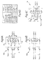
- Fig. 5 is a schematic circuit diagram of a fully differential sample and hold circuit to illustrate a first embodiment of the invention.
- circuit 100 includes only one operational amplifier and no resistors, where the remaining components are capacitors or switches.
- circuit 100 permits adjustments of the output in response to a single-ended input signal Vaux. Therefore, circuit 100 is advantageous over circuit 10 in that it requires much less area in the semiconductor medium and is more accurate.
- capacitors C1-C8 are assumed to have substantially the same capacitance C.
- S1 indicates a group of switches which are turned on at different times from the group S2 of switches. In the preferred embodiment illustrated in Fig. 5, switches S1 are turned on when the clock signal shown next to S1 in Fig. 2 and applied to S1 is high, but are turned off when such clock signal is low. Similarly, switches S2 of Fig. 5 are turned on when the corresponding clock signal is high but are turned off when such clock signal is low in Fig. 2. As shown in Fig. 2, the clock signals for operating switches S1, S2 do not overlap. As before, REZ(+), REZ(-) represent the return to zero positive and negative input signals in Fig. 5.
- circuit 100 is illustrated by means of the schematic circuit diagrams in Figs. 6A-6D, the table in Fig. 6D, and the timing diagram in Fig. 2.
- switches S1 are turned on and switches S2 are turned off in Fig. 5 so that circuit 100 becomes the same as circuit 100A in Fig. 6A.
- identical components in the figures of this application are labelled by the same reference symbols.
- the outputs SAM(+)' and SAM(-)' are at Vp, -Vp, respectively, the inputs REZ(+), REZ(-) inputs at V, -V, respectively, and a single-ended voltage Vaux is applied to capacitor C5 as shown in Fig. 6A.
- capacitors C1-C8 each has capacitance C. Therefore, the electrical charges on the lefthand and righthand plates of each of the eight capacitors are readily calculated for circuit 100A in Fig. 6A; the values of these charges are listed in the table in Fig. 6D.
- all the switches S1, S2 are open, so that circuit 100 of Fig. 5 becomes circuit 100B of Fig. 6B.
- the opening of switches S1 does not cause any current so that the electrical charges on both plates of the eight capacitors retain the values shown in the table of Fig. 6D.
- switches S2 are closed and switches S1 are open, so that circuit 100 of Fig. 5 becomes the same as circuit 100C of Fig. 6C.
- paths 102, 104 are connected respectively to the outputs 116, 118 of amplifier OP.
- the two paths 102, 104 are not connected to the amplifier at all.
- paths 102, 104 are connected to inputs 112, 114 respectively of the amplifier, instead of to the outputs.
- the righthand plate of C4 has an electrical charge whose value is -V-Vaux+2 ⁇ V.
- the output SAM(-)' is-V-Vaux+3 ⁇ V, since the amplifier OP introduces an additional offset voltage ⁇ V.
- circuit 100 in the above-described operation permits the adjustment of the potential difference between the two outputs by adding the auxiliary voltage Vaux.
- circuit 100 of Fig. 5 can be further simplified in the form of circuit 200 shown in Fig. 7, which is a schematic circuit diagram of a fully differential sample and hold circuit 200 to illustrate a second embodiment of the invention.
- circuit 200 in the abovedescribed control system again permits the differential output potential to be adjusted by adding Vaux thereto.
- circuit 200 In comparison to circuit 100 of Fig. 5, circuit 200 requires even fewer components and is therefore even cheaper to manufacture.
Landscapes
- Physics & Mathematics (AREA)
- Mathematical Physics (AREA)
- Engineering & Computer Science (AREA)
- Theoretical Computer Science (AREA)
- Software Systems (AREA)
- Computer Hardware Design (AREA)
- General Physics & Mathematics (AREA)
- Analogue/Digital Conversion (AREA)
- Amplifiers (AREA)
- Filters That Use Time-Delay Elements (AREA)
Claims (7)
- Circuit (100) échantillonneur-bloqueur totalement différentiel, pour ajouter un signal chaque fois unilatéral présentant une tension VAUX, à des signaux totalement différentiels (REZ(+), REZ(-)) présentant une tension V et -V respectivement, comprenant:un amplificateur opérationnel (OP) présentant une première et une deuxième sortie (116, 118) et une première et une deuxième entrée (112, 114);un moyen à capacité, comprenant plusieurs condensateurs (C1-C8); etdes moyens de commutation (S1, S2), pour relier le signal unilatéral et les signaux totalement différentiels aux moyens à capacité et à l'amplificateur, dans lequel les moyens de commutation (S1, S2) relient le signal unilatéral par l'intermédiaire de certains des condensateurs (C5) à une première sortie (116) de l'amplificateur à un premier instant (T1), et relient à un deuxième instant (T3) postérieur au premier instant, le signal unilatéral, par l'intermédiaire d'autres condensateurs (C6), à une deuxième entrée (114) d'amplificateur, de telle sorte que l'amplificateur délivre sur ses deux sorties deux signaux de sortie (SAM(+), SAM(-)) dont la différence est essentiellement aV+bVaux, où a, b sont des constantes.
- Circuit selon la revendication 1, comprenant en outre deux trajets de rétroaction, dans lequel un premier trajet de rétroaction comprend un condensateur (C3) pour relier la première entrée (112) et la première sortie (116), et un deuxième circuit de rétroaction comprend un condensateur (C4) pour relier la deuxième entrée (114) à la deuxième sortie (118).
- Circuit selon la revendication 2, dans lequel les moyens à capacité comprennent un premier condensateur (C1) et un deuxième condensateur (C5) pour coupler respectivement une première et une deuxième entrée du circuit à un premier trajet;
un troisième condensateur (C2) et un quatrième condensateur (C6) pour coupler une troisième et une quatrième entrée du circuit à un deuxième trajet; et un septième condensateur (C7) et un huitième condensateur (C8); dans lequel le moyen de commutation (S1) relie à un premier instant (T1) le signal différentiel (REZ(+)) présentant la tension V et le signal unilatéral présentant la tension Vaux respectivement à la première et à la deuxième entrée du circuit, raccorde respectivement le signal différentiel présentant la tension -V et une tension de référence à la troisième et à la quatrième entrée du circuit, branche le septième condensateur entre la première sortie de l'amplificateur et la tension de référence ou la première entrée de l'amplificateur, branche le huitième condensateur entre la deuxième sortie de l'amplificateur et la tension de référence ou la deuxième entrée de l'amplificateur, et relie le premier et le deuxième trajet respectivement à la première et à la deuxième sortie de l'amplificateur; et dans lequel le moyen de commutation (S2) relie à un deuxième instant (T3), la première, la deuxième et la troisième entrée du circuit à la tension de référence et la quatrième entrée du circuit au signal unilatéral présentant la tension Vaux, relie le premier et le deuxième trajet respectivement à la première et à la deuxième entrée de l'amplificateur, branche le septième condensateur entre la première entrée de l'amplificateur et la tension de référence et branche le huitième condensateur entre la deuxième entrée de l'amplificateur et la tension de référence, pour ainsi amener la différence de tension entre les deux sorties de l'amplificateur à essentiellement aV+bVaux, où a, b sont des constantes. - Circuit selon la revendication 3, dans lequel, à des instants (T2, T4) situés entre le premier et le deuxième instant, les moyens de commutation (S1, S2) amènent la déconnexion du premier, deuxième, troisième et quatrième condensateur des quatre entrées du circuit et du premier et du deuxième trajet, et déconnectent le septième et le huitième condensateur des entrées et des sorties de l'amplificateur.
- Circuit selon la revendication 3 ou la revendication 4, dans lequel au premier instant (T1), le moyen de commutation (S1) branche le septième condensateur (C7) entre la première sortie de l'amplificateur et la tension de référence, et branche le huitième condensateur (C8) entre la deuxième sortie de l'amplificateur et la tension de référence.
- Circuit selon l'une quelconque des revendications 3 à 5, dans lequel, au premier et au deuxième instant, le septième condensateur (C7) est directement relié à la première entrée de l'amplificateur, et le huitième condensateur (C8) est directement relié à la deuxième entrée de l'amplificateur.
- Circuit selon l'une quelconque des revendications précédentes, comprenant en outre un moyen pour fournir deux signaux d'horloge qui ne se superposent pas, pour faire fonctionner les moyens de commutation.
Priority Applications (4)
| Application Number | Priority Date | Filing Date | Title |
|---|---|---|---|
| CA002027083A CA2027083C (fr) | 1990-10-05 | 1990-10-05 | Circuit additionneur echantillonneur-bloqueur completement differentiel |
| US07/600,526 US5144160A (en) | 1990-10-05 | 1990-10-19 | Fully differential sample and hold adder circuit |
| DE69029391T DE69029391T2 (de) | 1990-10-05 | 1990-10-29 | Ganz differenzialer Abtast- und Haltkreisaddierer |
| EP90311817A EP0483419B1 (fr) | 1990-10-05 | 1990-10-29 | Circuit additionneur échantillonneur-bloqueur totalement différentiel |
Applications Claiming Priority (2)
| Application Number | Priority Date | Filing Date | Title |
|---|---|---|---|
| CA002027083A CA2027083C (fr) | 1990-10-05 | 1990-10-05 | Circuit additionneur echantillonneur-bloqueur completement differentiel |
| EP90311817A EP0483419B1 (fr) | 1990-10-05 | 1990-10-29 | Circuit additionneur échantillonneur-bloqueur totalement différentiel |
Publications (2)
| Publication Number | Publication Date |
|---|---|
| EP0483419A1 EP0483419A1 (fr) | 1992-05-06 |
| EP0483419B1 true EP0483419B1 (fr) | 1996-12-11 |
Family
ID=25674327
Family Applications (1)
| Application Number | Title | Priority Date | Filing Date |
|---|---|---|---|
| EP90311817A Expired - Lifetime EP0483419B1 (fr) | 1990-10-05 | 1990-10-29 | Circuit additionneur échantillonneur-bloqueur totalement différentiel |
Country Status (4)
| Country | Link |
|---|---|
| US (1) | US5144160A (fr) |
| EP (1) | EP0483419B1 (fr) |
| CA (1) | CA2027083C (fr) |
| DE (1) | DE69029391T2 (fr) |
Families Citing this family (20)
| Publication number | Priority date | Publication date | Assignee | Title |
|---|---|---|---|---|
| US5495192A (en) * | 1992-02-10 | 1996-02-27 | Yozan Inc. | Sample hold circuit |
| US5486785A (en) * | 1994-09-30 | 1996-01-23 | Mitsubishi Semiconductor America, Inc. | CMOS level shifter with feedforward control to prevent latching in a wrong logic state |
| JP2708007B2 (ja) * | 1995-03-31 | 1998-02-04 | 日本電気株式会社 | サンプル・ホールド回路 |
| US6147551A (en) * | 1998-01-05 | 2000-11-14 | Motorola, Inc. | Switched capacitor circuit and method for reducing sampling noise |
| US6031399A (en) * | 1998-02-13 | 2000-02-29 | National Semiconductor Corporation | Selectively configurable analog signal sampler |
| US6208542B1 (en) | 1998-06-30 | 2001-03-27 | Sandisk Corporation | Techniques for storing digital data in an analog or multilevel memory |
| EP1804251A3 (fr) * | 1998-06-30 | 2007-12-05 | SanDisk Corporation | Techniques pour stockage analogique à plusieurs niveaux utilisant un décalage ajustable de niveau de la tension d'entrée |
| US6486711B1 (en) * | 1998-07-15 | 2002-11-26 | Texas Instruments Incorporated | Capacitor-based exponential programmable gain amplifier |
| GB2368474A (en) * | 2000-09-28 | 2002-05-01 | Seiko Epson Corp | Sawtooth or triangular waveform generator |
| US6992509B2 (en) * | 2003-10-02 | 2006-01-31 | Supertex, Inc. | Switched-capacitor sample/hold having reduced amplifier slew-rate and settling time requirements |
| US7279940B1 (en) * | 2005-10-25 | 2007-10-09 | National Semiconductor Corporation | Switched-capacitor circuit with time-shifted switching scheme |
| DE102006014925B3 (de) * | 2006-03-30 | 2007-09-27 | Infineon Technologies Ag | Schaltungsanordnung mit einer Abtast-Halte-Einrichtung und Verfahren zur Signalverarbeitung in einer Abtast-Halte-Einrichtung |
| JP5062293B2 (ja) * | 2010-05-14 | 2012-10-31 | トヨタ自動車株式会社 | サンプルホールド回路及びa/d変換装置 |
| EP2437268B1 (fr) | 2010-09-30 | 2013-01-02 | ST-Ericsson SA | Circuit tampon d'extrémité unique à différentiel et procédé de couplage d'au moins un signal analogique d'entrée d'extrémité unique avec un circuit récepteur à entrées différentielles |
| JP2012249068A (ja) * | 2011-05-27 | 2012-12-13 | Toshiba Corp | 演算回路、及びa/d変換器 |
| US9519604B2 (en) * | 2014-04-11 | 2016-12-13 | Qualcomm Incorporated | Systems and methods for frequency control on a bus through superposition |
| US9438262B1 (en) * | 2015-06-22 | 2016-09-06 | Freescale Semiconductor, Inc. | Method for testing differential analog-to-digital converter and system therefor |
| CN106656072A (zh) * | 2016-12-31 | 2017-05-10 | 唯捷创芯(天津)电子技术股份有限公司 | 一种精确乘二开关电容放大器、芯片及通信终端 |
| US20250237682A1 (en) * | 2024-01-23 | 2025-07-24 | Qualcomm Incorporated | Measuring an open circuit voltage of a battery |
| CN121265071B (zh) * | 2025-12-05 | 2026-03-03 | 临港国家实验室 | 一种用于微弱生物电信号采集的设备 |
Family Cites Families (7)
| Publication number | Priority date | Publication date | Assignee | Title |
|---|---|---|---|---|
| US4553052A (en) * | 1982-04-23 | 1985-11-12 | Nec Corporation | High speed comparator circuit with input-offset compensation function |
| US4587443A (en) * | 1984-08-27 | 1986-05-06 | Signetics Corporation | Auto-zero sample and hold circuit |
| JPS6276099A (ja) * | 1985-09-30 | 1987-04-08 | Toshiba Corp | サンプル・アンド・ホ−ルド回路 |
| US4707624A (en) * | 1986-09-10 | 1987-11-17 | National Semiconductor Corp. | Offset cancellation scheme for a differential reset stabilized latch |
| DE3723919A1 (de) * | 1987-07-18 | 1989-01-26 | Philips Patentverwaltung | Vergleichsschaltung |
| FR2641924B1 (fr) * | 1988-12-28 | 1991-05-03 | Sgs Thomson Microelectronics | Generateur de forme d'onde de signal analogique |
| US5028815A (en) * | 1989-01-16 | 1991-07-02 | U. S. Philips Corporation | Clocked comparator with offset reduction |
-
1990
- 1990-10-05 CA CA002027083A patent/CA2027083C/fr not_active Expired - Fee Related
- 1990-10-19 US US07/600,526 patent/US5144160A/en not_active Expired - Lifetime
- 1990-10-29 DE DE69029391T patent/DE69029391T2/de not_active Expired - Fee Related
- 1990-10-29 EP EP90311817A patent/EP0483419B1/fr not_active Expired - Lifetime
Also Published As
| Publication number | Publication date |
|---|---|
| US5144160A (en) | 1992-09-01 |
| DE69029391D1 (de) | 1997-01-23 |
| DE69029391T2 (de) | 1997-04-24 |
| EP0483419A1 (fr) | 1992-05-06 |
| CA2027083C (fr) | 1996-05-28 |
| CA2027083A1 (fr) | 1992-04-06 |
Similar Documents
| Publication | Publication Date | Title |
|---|---|---|
| EP0483419B1 (fr) | Circuit additionneur échantillonneur-bloqueur totalement différentiel | |
| US6437720B1 (en) | Code independent charge transfer scheme for switched-capacitor digital-to-analog converter | |
| US4543534A (en) | Offset compensated switched capacitor circuits | |
| US5490099A (en) | Method of multiplying an analog value by a digital value | |
| US4404525A (en) | Switched capacitor gain stage with offset and switch feedthrough cancellation scheme | |
| US4835482A (en) | Semiconductor integrated circuit forming a switched capacitor filter | |
| EP0508360B1 (fr) | Circuit référence de tension échantillonnée de type band-gap | |
| US5220286A (en) | Single ended to fully differential converters | |
| US5359294A (en) | Charge-balanced switched-capacitor circuit and amplifier circuit using same | |
| JPH0322103B2 (fr) | ||
| JP2726413B2 (ja) | 振幅比較回路 | |
| CA1234415A (fr) | Filtre capacitif commute | |
| US5381053A (en) | Voltage comparator circuit capable of avoiding erroneous operation | |
| EP0158646B1 (fr) | Circuits a condensateurs commutes | |
| EP0340439A2 (fr) | Circuit amplificateur à condensateurs commutés | |
| US5420807A (en) | Multiplication circuit for multiplying analog inputs by digital inputs | |
| US4585951A (en) | Precision triangle waveform generator | |
| EP0322963A1 (fr) | Circuit de condensateurs commutables | |
| US5973537A (en) | Common mode control circuit for a switchable fully differential Op-AMP | |
| US4517551A (en) | Digital to analog converter circuit | |
| EP0460651B1 (fr) | Convertisseur numérique-analogique | |
| GB2111780A (en) | Improvements in or relating to amplifier systems | |
| KR850007721A (ko) | 신호비교회로 및 그 방법과 리미터 및 신호처리기 | |
| US4559498A (en) | Symmetrical integrator and application of said integrator to an electric filter | |
| US6404262B1 (en) | Switched capacitor integrator using unity gain buffers |
Legal Events
| Date | Code | Title | Description |
|---|---|---|---|
| PUAI | Public reference made under article 153(3) epc to a published international application that has entered the european phase |
Free format text: ORIGINAL CODE: 0009012 |
|
| AK | Designated contracting states |
Kind code of ref document: A1 Designated state(s): DE FR GB IT |
|
| 17P | Request for examination filed |
Effective date: 19920924 |
|
| 17Q | First examination report despatched |
Effective date: 19950130 |
|
| GRAH | Despatch of communication of intention to grant a patent |
Free format text: ORIGINAL CODE: EPIDOS IGRA |
|
| GRAH | Despatch of communication of intention to grant a patent |
Free format text: ORIGINAL CODE: EPIDOS IGRA |
|
| GRAA | (expected) grant |
Free format text: ORIGINAL CODE: 0009210 |
|
| AK | Designated contracting states |
Kind code of ref document: B1 Designated state(s): DE FR GB IT |
|
| PG25 | Lapsed in a contracting state [announced via postgrant information from national office to epo] |
Ref country code: IT Free format text: LAPSE BECAUSE OF FAILURE TO SUBMIT A TRANSLATION OF THE DESCRIPTION OR TO PAY THE FEE WITHIN THE PRE;WARNING: LAPSES OF ITALIAN PATENTS WITH EFFECTIVE DATE BEFORE 2007 MAY HAVE OCCURRED AT ANY TIME BEFORE 2007. THE CORRECT EFFECTIVE DATE MAY BE DIFFERENT FROM THE ONE RECORDED.SCRIBED TIME-LIMIT Effective date: 19961211 Ref country code: FR Effective date: 19961211 |
|
| REF | Corresponds to: |
Ref document number: 69029391 Country of ref document: DE Date of ref document: 19970123 |
|
| EN | Fr: translation not filed | ||
| PLBE | No opposition filed within time limit |
Free format text: ORIGINAL CODE: 0009261 |
|
| STAA | Information on the status of an ep patent application or granted ep patent |
Free format text: STATUS: NO OPPOSITION FILED WITHIN TIME LIMIT |
|
| PG25 | Lapsed in a contracting state [announced via postgrant information from national office to epo] |
Ref country code: GB Free format text: LAPSE BECAUSE OF NON-PAYMENT OF DUE FEES Effective date: 19971029 |
|
| 26N | No opposition filed | ||
| GBPC | Gb: european patent ceased through non-payment of renewal fee |
Effective date: 19971029 |
|
| PGFP | Annual fee paid to national office [announced via postgrant information from national office to epo] |
Ref country code: DE Payment date: 20031201 Year of fee payment: 14 |
|
| PG25 | Lapsed in a contracting state [announced via postgrant information from national office to epo] |
Ref country code: DE Free format text: LAPSE BECAUSE OF NON-PAYMENT OF DUE FEES Effective date: 20050503 |